

Page 1

TECHNICAL
MANUAL
HT EL2000LS/HS
994 9383 001 - HT EL2000LS
994 9384 001 - HT EL2000HS
TECHNICAL MANUAL
HT EL2000LS/HS
994 9383 001 - HT EL2000LS
994 9384 001 - HT EL2000HS
888-2457-001
I Installation
II Operation
III Theory of Operation
IV Maintenance & Alignments
V Troubleshooting
VI Parts List
Transmitter
PA Amplifier Modules
VII RF Amplifier Modules
T.M. No. 888-2457-001
© Copyright 1999, 2002, 2003
Harris Corporation
All rights reserved
Rev. B: 7-25-02
Rev. B1: 6-02-03
Page 2

Returns And Exchanges
Damaged or undamaged equipment should not be returned unless written approval and a
Return Authorization is r eceived from HARRIS CORPORATION, Broadcast Systems Division. Special shipping instructions and coding will be provided to as sure proper handling.
Complete details regarding circumstances and reasons for return are to be included in the
request for return. Custom equipment or special order equipment is not returnable. In those
instances where return or exchange of equipment is at the request of the customer, or
convenience o f the customer, a restocking fee will be charged. All returns will be sent
freight prepaid and properly insured by the customer. When communicating with HARRIS
CORPORATION, Broadcast Systems Division, specify the HARRIS Order N umber or Invoice Number.
Unpacking
Carefully unpack the equipment and preform a visual inspection to determine that no apparent damage was incurred during shipment. Retain the shipping materials until it has been
determined that all received equipment is not damaged. Locate and retain all PACKING
CHECK LISTs. Use the PACKING CHECK LIST to help locate and identify any components
or assemblies which are removed for shipping and must be reinstalled. Also remove any
shipping supports, straps, and packing materials prior to initial turn on.
Technical Assistance
HARRIS Technical and Troubleshooting assistance is available from HARRIS Field Service
during normal business hours (8:00 AM - 5:00 PM Central Time). Emergency service is
available 24 hours a day. Telephone 217/222-8200 to contact the Field Service Department
or address correspondence to Field Service Department, HARRIS CORPORATION, Broadcast Systems Division, P.O. Box 4290, Quincy, Illinois 62305-4290, USA. Technical Support
by e-mail: tsupport@harris.com. The HARRIS factory may also be contacted through a FAX
facility (217/221-7096).
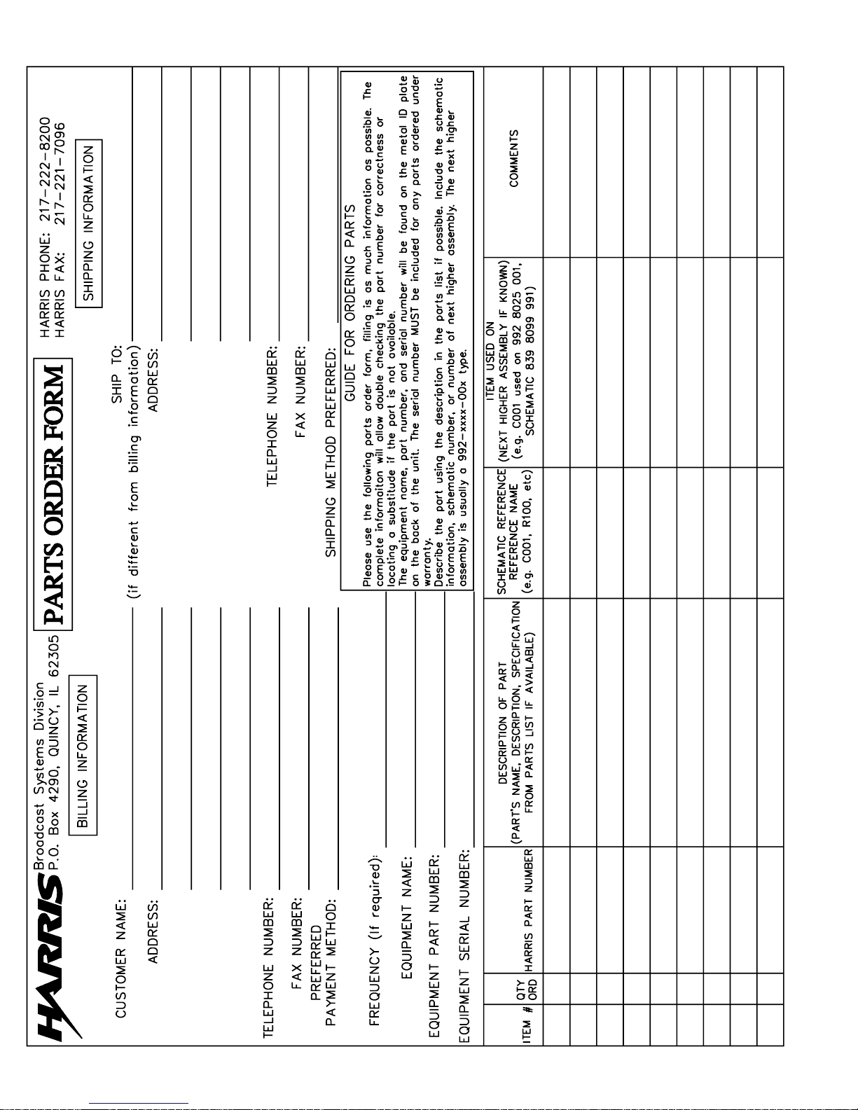
Replaceable Parts Service
Replacement parts are available 24 hours a day, seven days a week from the HARRIS
Service Parts Department. Telephone 217/222-8200 to contact the service parts department
or address correspondence to Service Parts Department, HARRIS CORPORATION, Broadcast Systems Division, P.O. Box 4290, Quincy, Illinois 62305-4290, USA. The HARRIS factory may also be contacted through a FAX facility (217/221-7096).
NOTE
The # symbol used in the parts list means used with (e.g. #C001 = used with C001).
Page 3

MANUAL REVISION HISTORY
888-2457-001
Rev. Date ECN Pages Changed
001-B 7/25/02 48420 Replaced Title Page, iv, and 4-6
Added MRH-1/MRH-2
WARNING: Disconnect primary power prior to servicing.
888-2457-001 MRH-1/MRH-1
Page 4

This page left blank intentionally
Page 5
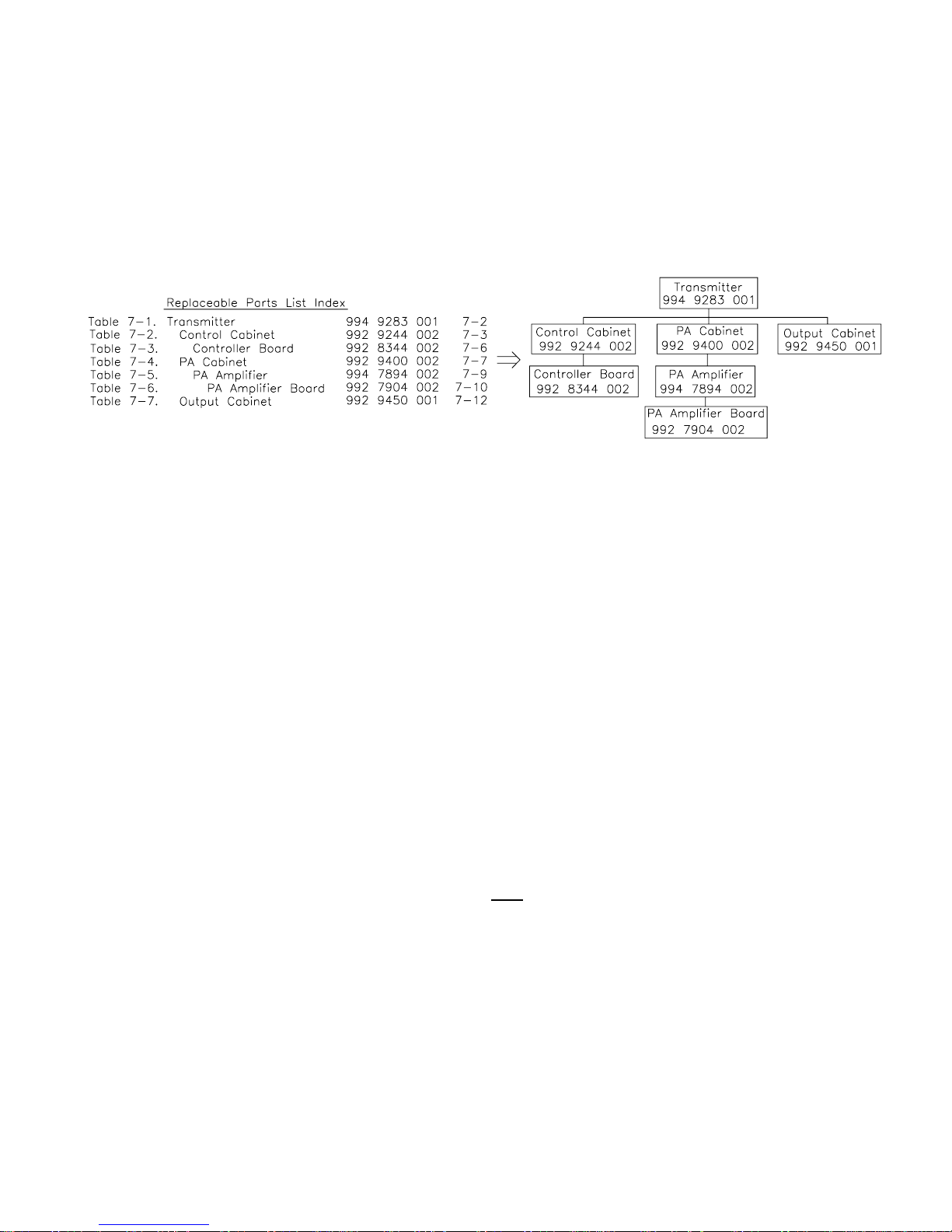
Guide to Using Harris Parts List Information
The Harris Replaceable Parts List Index portrays a tree structure with the major items being leftmost in the index.
The example below shows the Transmitter as the highest item in the tree structure. If you were to look at the bill of
materials table for the Transmitter you would find the Control Cabinet, the PA Cabinet, and the Output Cabinet. In
the Replaceable Parts List Index the Control Cabinet, PA Cabinet, and Output Ca binet show up one indentation level
below the Transmitter and implies that they are used in the Transmitter. The Controller Board is indented one level
below the Control Cabinet so it will show up in the bill of material for the Control Cabinet. The tree structure of this
same index is shown to the right of the table and shows indentation level versus tree structure level.
Example of Replaceable Parts List Index and equivalent tree structure:
The part number of the item is shown to the right of the description as is the page in the manual where the bill for
that part number starts.
Inside the actual tables, four main headings are used:
Table #-#. ITEM NAME - HARRIS PART NUMBER - this line gives the information that corresponds to the
Replaceable Parts List Index entry;
HARRIS P/N column gives the ten digit Harris part number (usually in ascending order);
DESCRIPTION column gives a 25 character or less description of the part number;
REF. SYMBOLS/EXPLANATIONS column 1) gives the reference designators for the item (i.e., C001, R102,
etc.) that corresponds to the number found in the schematics (C001 in a bill of material is equivalent to C1 on the
schematic) or 2) gives added information or further explanation (i.e., “Used for 208V operation only,” or “Used
for HT 10LS only,” etc.).
Inside the individual tables some standard conventions are used:
A # symbol in front of a component such as #C001 under the REF. SYMBOLS/EXPLANATIONS column means
that this item is used on or with C001 and is not the actual part number for C001.
In the ten digit part numbers, if the last three numbers are 000, the item is a part that Harris has purchased and
has not manufactured or modified. If the last three numbers are other than 000, the item is either manufactured by
Harris or is purchased from a vendor and modified for use in the Harris product.
The first three digits of the ten digit part number tell which family the part number belongs to - for example, all
electrolytic (can) capacitors will be in the same family
(524 xxxx 000). If an electrolytic (can) capacitor is found
to have a 9xx xxxx xxx part number (a number outside of the normal family of numbers), it has probably been
modified in some manner at the Harris factory and will therefore show up farther down into the individual parts
list (because each table is normally sorted in ascending order). Most Harris made or modified assemblies will
have 9xx xxxx xxx numbers associated with them.
The term “SEE HIGHER LEVEL BILL” in the description column implies that the reference designated part
number will show up in a bill that is higher in the tree structure. This is often the case for components that may
be frequency determinant or voltage determinant and are called out in a higher level bill structure that is more
customer dependent than the bill at a lower level.
2-02-93
Page 6
Page 7

WARNING
THE CURRENTS AND VOLTAGES IN THIS EQUIPMENT ARE DANGEROUS. PERSONNEL MUST AT ALL TIMES OBSERVE SAFETY WARNINGS, INSTRUCTIONS
AND REGULATIONS.
This manual is intended as a general guide for trained and qualified personnel who are aware of the dangers inherent in
handling potentially hazardous electrical/electronic circuits. It is not intended to contain a complete statement of all safety
precautions which should be observed by personnel in using this or other electronic equipment.
The installation, operation, maintenance and service of this equipment involves risks both to personnel and equipment, and
must be performed only by qualified personnel exercising due care. HARRIS CORPORATION shall not be responsible for
injury or damage resulting from improper procedures or from the use of improperly trained or inexperienced personnel
performing such tasks.
During installation and operation of this equipment, local building codes and fire protection standards must be observed.
The following National Fire Protection Association (NFPA) standards are recommended as reference:
- Automatic Fire Detectors, No. 72E
- Installation, Maintenance, and Use of Portable Fire Extinguishers, No. 10
- Halogenated Fire Extinguishing Agent Systems, No. 12A
WARNING
ALWAYS DISCONNECT POWER BEFORE OPENING COVERS, DOORS, ENCLOSURES, GATES, PANELS OR SHIELDS. ALWAYS USE GROUNDING STICKS AND
SHORT OUT HIGH VOLTAGE POINTS BEFORE SERVICING. NEVER MAKE INTERNAL ADJUSTMENTS, PERFORM MAINTENANCE OR SERVICE WHEN ALONE
OR WHEN FATIGUED.
Do not remove, short-circuit or tamper with interlock switches on access covers, doors, enclosures, gates, panels or shields.
Keep away from live circuits, know your equipment and don’t take chances.
WARNING
IN CASE OF EMERGENCY ENSURE THAT POWER HAS BEEN DISCONNECTED.
WARNING
IF OIL FILLED OR ELECTROLYTIC CAPACITORS ARE UTILIZED IN YOUR
EQUIPMENT, AND IF A LEAK OR BULGE IS APPARENT ON THE CAPACITOR
CASE WHEN THE UNIT IS OPENED FOR SERVICE OR MAINTENANCE, ALLOW
THE UNIT TO COOL DOWN BEFORE ATTEMPTING TO REMOVE THE DEFECTIVE CAPACITOR. DO NOT ATTEMPT TO SERVICE A DEFECTIVE CAPACITOR
WHILE IT IS HOT DUE TO THE POSSIBILITY OF A CASE RUPTURE AND SUBSEQUENT INJURY.
i
Page 8
ii
Page 9

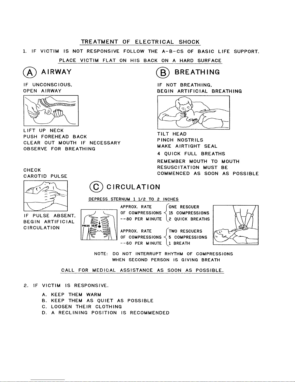
FIRST-AID
Personnel engaged in the installation, operation, maintenance or servicing of this equipment are urged to become familiar
with first-aid theory and practices. The following information is not intended to be complete first-aid procedures, it is a
brief and is only to be used as a reference. It is the duty of all personnel using the equipment to be prepared to give
adequate Emergency First Aid and thereby prevent avoidable loss of life.
Treatment of Electrical Burns
1. Extensive burned and broken skin
a. Cover area with clean sheet or cloth. (Cleanest available cloth article.)
b. Do not break blisters, remove tissue, remove adhered particles of clothing, or apply any salve or ointment.
c. Treat victim for shock as required.
d. Arrange transportation to a hospital as quickly as possible.
e. If arms or legs are affected keep them elevated.
NOTE
If medical help will not be available within an hour and the victim is
conscious and not vomiting, give him a weak solution of salt and soda:
1 level teaspoonful of salt and 1/2 level teaspoonful of baking soda to
each quart of water (neither hot or cold). Allow victim to sip slowly
about 4 ounces (a half of glass) over a period of 15 minutes. Discontinue fluid if vomiting occurs. (Do not give alcohol.)
REFERENCE:
2. Less severe burns - (1st & 2nd degree)
a. Apply cool (not ice cold) compresses using the cleanest available cloth article.
b. Do not break blisters, remove tissue, remove adhered particles of clothing, or apply salve or ointment.
c. Apply clean dry dressing if necessary.
d. Treat victim for shock as required.
e. Arrange transportation to a hospital as quickly as possible.
f. If arms or legs are affected keep them elevated.
ILLINOIS HEART ASSOCIATION
AMERICAN RED CROSS STANDARD FIRST AID AND PERSONAL SAFETY MANUAL (SECOND EDITION)
iii
Page 10

Table Of Contents
Section I
Introduction/Specifications
Introduction......................................1-1
GeneralDescription .............................1-1
ControlandMonitoring ............................1-1
Signal Flow Through the System..................... 1-1
RFAmplifierModules............................. 1-1
PowerSupplies...................................1-1
Cooling .........................................1-1
RFOutputSystem.................................1-1
OptionalEquipment ...............................1-1
BlockDiagram ...................................1-1
Specifications ....................................1-1
Section II
Installation
Introduction......................................2-1
TestEquipmentRequirementPlanning.............. 2-1
MechanicalInstallationPlanning.....................2-1
SpaceRequirements............................. 2-1
ApproximateShippingWeights....................2-1
RFSystemLayout ..............................2-1
AirSystem.....................................2-1
ElectricalInstallationPlanning.......................2-1
PowerRequirements.............................2-1
CircuitBreakerSelection.........................2-1
ACmainsDisconnectLocation....................2-2
UnloadingandUnpacking..........................2-2
EquipmentRequiredforUnloading.................2-2
Unpacking,EquipmentInventoryandInspection......2-2
FactoryTestDataSheets .........................2-3
CabinetPlacementandLeveling................... 2-3
ElectricalInstallation ..............................2-4
Grounding .....................................2-4
PrimaryWiring................................. 2-4
SettingTransformersTaps........................2-5
Input Signals ...................................2-5
SetupJumpers..................................2-5
BackupBattery.................................2-5
RFOutputCoaxConnections...................... 2-5
Interlocks......................................2-5
TransmitterCheckOut............................. 2-5
Pre-turnonchecks .............................. 2-5
InitialTurn-onSequence .........................2-5
Module Installation..............................2-5
ControlSystemCheckOut........................2-6
InitialApplicationofRFPower....................2-6
Visual.....................................2-6
Aural .........................................2-6
RemoteControlInputandOutput.................... 2-6
CommandIn1A12J21 ...........................2-6
1A12J22:StatusOutputs .........................2-6
StatusFunctions1A12J22 ........................2-7
AnalogOutputs1A12J23......................... 2-7
Section III
Operation
Introduction......................................3-1
ControlsAndIndicators............................ 3-1
LocalTurn-onandTurn-off ........................ 3-1
VideoControlledOperation ........................ 3-1
RemoteControl/ExtendedOperation................. 3-1
Section IV
Theory of Operation
Introduction ..................................... 4-1
SystemOverview................................. 4-1
Exciter,MeterandControlBoard.................... 4-1
A/D&Displays................................ 4-1
BarGraphDisplay.............................. 4-1
AnalogMultiplexers ............................ 4-1
MeterSelector................................. 4-1
LossOfVideoDelayDetector.................... 4-2
Override/NormalSelection....................... 4-2
ClockCircuits ................................. 4-2
BATTERY (BAT) SUPPLY VOLTAGE............ 4-2
VisualPowerControl ........................... 4-2
AuralPowerControl............................ 4-2
PowerUpReset................................ 4-2
JP2&JP3..................................... 4-2
FREQUNLOCK............................... 4-2
VIS_CLK_GATE U18 & AUR_CLK_GATE U19
FunctionalDescriptions......................... 4-3
METER_CLK_GATE U20 Functional De-
scriptions................................. 4-3
METER_SEL U17 Functional Descriptions.......... 4-3
VIS_UP/DWN_PWR_CTRLU26&U27....... 4-3
VisualDACU25............................... 4-3
VisualFoldbackControl......................... 4-3
AUR_UP/DWN_PWR_CTRLU29&U30.......... 4-3
InterfaceLogicModule............................ 4-4
PeakDetectors................................. 4-4
FoldbackCircuits............................... 4-4
HighVSWR................................... 4-5
Command Input Logic PAL U8 (917-2321-004)...... 4-5
XMTRCTRLPALU15 ..................... 4-5
Fault Encoder U19 (917-2321-008) ............ 4-5
50VOK .................................. 4-5
AirFault.................................. 4-6
ACBREAKERS ................................. 4-6
MAINBREAKER.............................. 4-6
ACCONTROLBREAKER...................... 4-6
LOGICSUPPLYBREAKER..................... 4-6
POWER MODULE 1A11 .......................... 4-6
POWER SUPPLY FAULT DISPLAY and INTER-
FACE1A11A6................................ 4-6
50VSUPPLIES1A11A1and1A11A5 ............. 4-7
LOGICSUPPLY1A11A3 ....................... 4-7
Section V
Maintenance and Alignments
Introduction ..................................... 5-1
StationRecords .................................. 5-1
Transmitter Logbook ............................ 5-1
MaintenanceLogbook........................... 5-1
SafetyPrecautions.............................. 5-1
PreventiveMaintenance ........................... 5-1
AirFilterMaintenance .......................... 5-1
iv 888-2457-001 Rev. B: 7/25/02
WARN9ING: Disconnect primary power prior to servicing.
Page 11

MOV’S....................................... 5-2
Semiconductors................................ 5-2
Capacitors................................. 5-2
FixedResistors............................. 5-2
Transformers .............................. 5-2
Relays.................................... 5-2
PerformanceChecks.............................. 5-2
Adjustments..................................... 5-2
RFPowerMeasurements .......................... 5-2
Through-LineMeters............................ 5-2
Visual Peak-sync to Average Power Conversion For-
mulas........................................ 5-3
TransmitterMeteringandControlCalibration.......... 5-3
Power Supply Meter Calibration................... 5-3
PSVOLTSCalibration:...................... 5-3
PSCURRENTCalibration ................... 5-3
ExciterRFOutputMeterCalibration............... 5-3
ExciterVisualPowerCalibration.............. 5-3
ExciterAuralPowerCalibration............... 5-3
TransmitterRFOutputMeterCalibration ........... 5-3
Transmitter Visual Forward Power Calibra-
tion...................................... 5-4
Transmitter Visual Reflected Power Calibra-
tion...................................... 5-4
TransmitterAuralForwardPowerCalibration.... 5-4
Transmitter Aural Reflected Power Calibra-
tion...................................... 5-4
VSWRFaultAndFoldbackAdjustments ........... 5-4
InitialSetupforAdjustment .................. 5-4
VisualHighVSWRAdjustment............... 5-4
VisualVSWRFoldbackAdjustment ........... 5-4
AURALHIGHVSWRAdjustment............ 5-4
AuralVSWRFoldbackAdjustment............ 5-4
TransmitterAGCAdjustment....................... 5-4
VisualAGC: .................................. 5-4
VisualPowerReduction......................... 5-5
AuralAGC.................................... 5-5
AuralPowerReduction.......................... 5-5
Component Replacement On Circuit Boards ........... 5-5
Section VI
Troubleshooting
Introduction..................................... 6-1
Troubleshooting Assistance......................... 6-1
Returns......................................... 6-1
Section VII
Parts List
Section VIII
Parts List
Appendix A
RF Amplifier M odules, Platinum Series
GeneralInformation .............................. A-1
Factory Module Repair .......................... A-1
LocalModuleRepair............................ A-1
RFAmplifierModulesTheoryofOperation........... A-1
Driver Module, Low Band........................A-2
Driver Module, High Band .......................A-2
PAModule....................................A-4
RF Quarter Modules.............................A-4
Low Band Quarter Module .......................A-4
HighBandQuarterModule.......................A-5
Quarter Module Bias ............................A-5
Protection,ControlandMonitorSubsystem..........A-5
Module Status LEDs ............................A-6
RedLEDFaultBlinkCodes ..................A-6
Module Troubleshooting ...........................A-6
Platinum™ TV Module Test Fixture (992-8556-002) . . A-7
Troubleshooting Based on Module Swapping ........A-7
Troubleshooting Based on Module Blink Codes ......A-7
IsolatingOtherFailures.........................A-10
LocatingFailedRFFETs........................A-11
DCResistanceTest.........................A-11
IdleCurrentTest...........................A-11
PartsReplacementProcedures......................A-12
SolderingPrecautions...........................A-12
Quarter Module Replacement ....................A-13
RFFETReplacement...........................A-13
TestingandReplacingIsolationResistors ..........A-14
PassFETReplacement..........................A-14
ChipCapReplacement .........................A-15
TestProcedureSolidStateTVModules..............A-15
Pre-operationalChecks .........................A-15
InitialPowerUp...........................A-15
IdleCurrentCheck.........................A-15
Over/UnderVoltageCheck..................A-15
RFTesting ...................................A-15
ApplicationofDrive........................A-15
GainCheck...............................A-15
Alternate method for measurement under
program conditions......................A-16
ISOVoltsCheck...........................A-16
OverdriveCheck...........................A-16
VSWRCheck.............................A-16
Appendix B
Air Conditioning Considerations
Air Conditioning ................................. B-1
HeatLoadEstimateGuide.......................... B-1
Appendix C
Surge and Lightning Protection and Grounding Consid-
erations
SurgeandLightningProtection...................... C-1
System Grounding ................................ C-1
Ground Wires .................................. C-1
ACGround....................................C-1
DCGround....................................C-2
Earth Ground ..................................C-2
RF Ground .................................... C-2
Rev. B: 7/25/02 888-2457-001 v
WARN9ING: Disconnect primary power prior to servicing.
Page 12

This page left blank intentionally
Page 13

Section I
Introduction/Specifications
1.1 Introduction
1.1.1 General Description
Platinum™ Series The HT EL 2000 watt television transmitter
is an externally diplexed transmitter available in CCIR systems
forM,D/K,B,I,andK.
The transmitter consistsof5 RFamplifier modules, coolingfans,
50 volt power supplies,controlinterface tray,logicpower supply
and an exciter. The exciter includes thetransmitter controlpanel.
Transmitters operate on a 208-240 volt single phase 50 or 60
Hertz. The transmitter assemblies all are mounted in a single
cabinet 183 cm (72 inches) high.
1.2 Control and Monitoring
Transmitters are designed for local, video present control, or
remote/extended operation. VSWR foldback is used to protect
the transmitter RF system. Over temperature protection of RF
modules and module power supplies is standard.
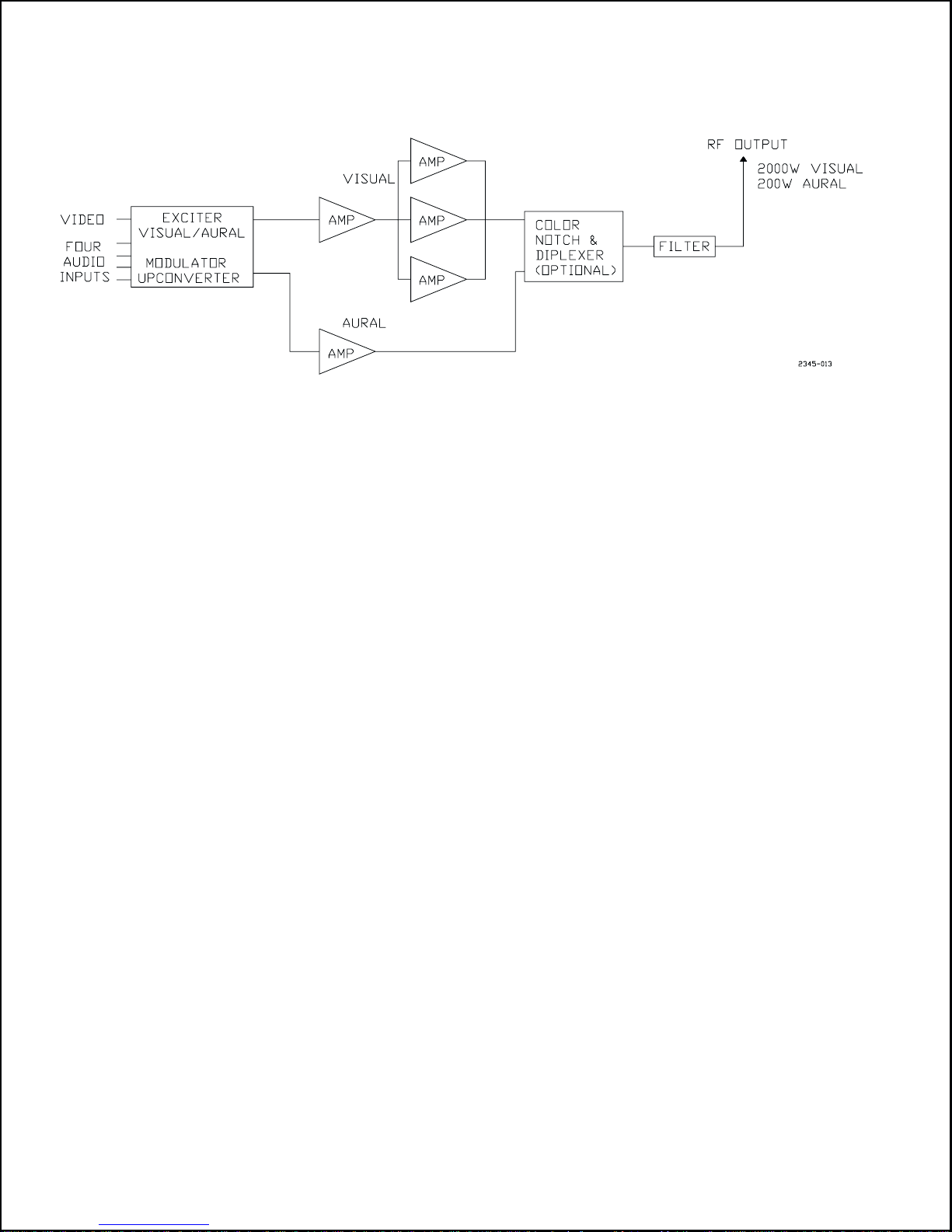
1.3 Signal Flow Through the System
Refer to transmitter block diagram Figure 1-1.
The visual exciter uses IF modulation with pre-correction at
video and IF. The visual signal is amplified by a driverand three
PA modules.
The aural exciter modulates audio baseband and subcarrier inputs at aural IF carrier . Optional IF group delay correction is
available for a Notch Diplexer and aural linearization for dual
carrier systems. The aural signal is amplified by a RF driver
amplifier module.
1.6 Cooling
The main coolingair intake isthrough the reardoor and exhausts
out the top and right side. There are fivesupply and five exhaust
fans for module cooling. T wo other fans are used for heat pipe
cooling.
Removing one module will not affect air flow to other modules.
Each power supply has a fan to draw air from the front of the
transmitter.
1.7 RF Output System
Various diplexing systems are used as the system requires. Harmonic and imagefrequency color subcarrierfiltersare part ofthe
system.
1.8 Optional Equipment
Single or dual cavity Notch Diplexer
Multichannelsound:NICAM, IRTDual Carrierand BTSC
Precision Offset
Combined transmitters
Main/alternate transmitters
Second exciter with automatic exciter switcher
Power measurement wattmeter
RF module test fixture
Spare parts, semiconductors and board assemblies
Spare RF modules
Transmitter Remote Control System
1.9 Block Diagram
Figure 1-1 is a block diagram of the HT EL2000LS/HS.
1.4 RF Amplifier Modules
Like aural and visual modules are interchangeable and have
overdrive, over/undervoltage, power unbalance, VSWR, and
overtemperature protection. The modules may be repaired in the
field at the quarter module or component level.
1.5 Power Supplies
The exciter and interface logic utilize linear regulator supplies.
The RF module power comes from power factor corrected
switching supplies in the power module assembly.
WARNING: Disconnect primary power prior to servicing.
1.10 Specifications
Table 1-1 lists the specificaitons for the HT EL2000LS/HS.
NOTE
Specifications subject to change without notice.
888-2457-001 1-1
Page 14
Platinum™ Series
Figure 1-1. HT EL2000 LS/HS Block Diagram
1-2 888-2457-001
WARNING: Disconnect primary power prior to servicing.
Page 15
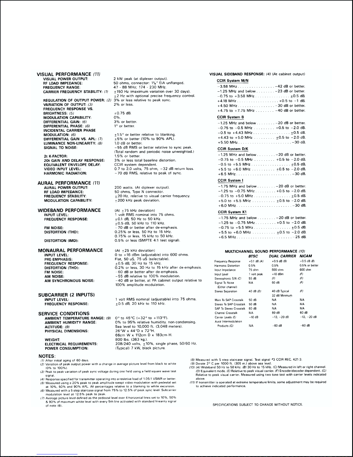
Table 1-1. Specifications
Section I - Introduction/Specifications
WARNING: Disconnect primary power prior to servicing.
888-2457-001 1-3
Page 16

Platinum™ Series
Table 1-1. Specifications
Electrical Specifications HT EL2000LS/HS
V isual Specifications:
Power Output 2 kW Peak of sync
Measured at output of optional diplexer
Frequency Range HT EL2000LS, 47-88 MHz
HT EL2000HS, 170-230 MHz
Systems CCIR-M,N,B,D/K,K1,I
Color Formats NTSC, PAL, SECAM
RF Output:
Impedance 50 ohms.
Connector 1 5/8" EIA unflanged
Video Input:
Impedance 75 Ohm, 32 dB return loss up to 5.0 MHz
Level 0.5 - 2.0 Volts, peak to peak
Visual Modulation Capability 0%
Measured using synchronous detector.
Frequency Response vs. Brightness 0.75 dB or better
Measured using a 20% amplitude swept video modulation with pedestal set at
10%, 50% and 90% APL. All percentages relative to a blanking to white
excursion.
Differential Gain 3% or better
Measured with a 5-step staircase signal 0 to 100 IRE units and color subcarrier
of 20 IRE units peak to peak.
Differential Phase 1 or better
Measured with 5-step staircase signal as in Differential Gain.
Incidental Carrier Phase Modulation 1.5 or better
Carrier phase variation from reference white to sync tip relative to blanking.
Luminance Non-linearity 1.0 dB or better
Measured with a 5-step staircase signal. Test Signal #3 CCIR Rec. 421-3.
Equivalent Envelope Delay Compliant with CCIR system
2T Pulse K-Factor 1.5% Maximum
20T Pulse 3% Maximum baseline disturbance
Signal-to-Noise -55 dB RMS or better
Total random and periodic noise unweighted, relative to peak sync.
Variation of Output 2% or less
Total peak-to-peak variation of peak sync voltage during one field, using a field
square wave test signal.
Regulation of Output Power 3% or less
Variation of peak output power with a change in average picture level from
black to white (0% to 100%).
Carrier Frequency Stability 150 Hz per month
After 60 day initial aging.
(2 Hz, with optional precise frequency control)
Harmonic Radiation -70 dB RMS, relative to peak vision power.
Aural Specifications:
1-4 888-2457-001
WARNING: Disconnect primary power prior to servicing.
Page 17

Table 1-1. Specifications
Continued
Power Output 200 W
Measured at output of optional notch diplexer.
RF Output:
Impedance 50 Ohms
Connector Type N, Female
Audio Inputs:
1. Monaural
Level 0 to +16 dBm, 25 kHz deviation
Impedance 600 Ohms balanced
Response 0.5 dB, 30 Hz-15 kHz
Pre-emphasis Flat / 50uS / 75uS, selectable
2. Subcarrier (2 inputs)
Level 1 volt RMS, adjustable.
Impedance 75 Ohms, unbalanced
Response 0.5 dB, 20 kHz-110 kHz.
3. Wideband(composite)
Level 1 volt RMS nominal for 75 kHz deviation
Impedance 75 Ohms, unbalanced
Response 0.1 dB, 50 Hz to 50 kHz
0.5 dB, 50 kHz to 110 kHz
Monaural Performance:
Frequency Response 0.5 dB, 30 Hz to 15 kHz
Relative to standard 75S or 50S pre-emphasis curve.
Harmonic Distortion 0.2% or less
Measured at 25 kHz deviation, 30 Hz to 15 kHz after de-emphasis.
FM Signal-to-Noise 60 dB RMS or better
Relative to 25 kHz deviation.
AM Signal-to-Noise 55 dB RMS or better
Relative to 100% amplitude modulation.
AM Synchronous Noise 40 dB RMS or better
Relative to 100% amplitude modulation, measured before optional diplexer.
Wideband Composite Performance: (At 75kHz deviation)
Harmonic Distortion 0.25% or less, 50 Hz to 15 kHz
0.75% or less, 15 kHz to 50 kHz
Distortion (IMD) 0.5% or less
SMPTE 4:1 test signal.
FM Signal-to-Noise 70 dB RMS or better
Measured after de-emphasis.
AM Signal-to-Noise 55 dB RMS or better
Relative to 100% amplitude modulation.
AM Synchronous Noise 40 dB RMS or better
Relative to 100% amplitude modulation.
Stereo Separation 45 dB or better ,50 Hz to 15 kHz
Equivalent mode (uncompanded).
Crosstalk 50 dB or better
Stereo or Main channel into SAP.
Mechanical, Environment, Power
Physical Dimensions:
Section I - Introduction/Specifications
WARNING: Disconnect primary power prior to servicing.
888-2457-001 1-5
Page 18

Platinum™ Series
Table 1-1. Specifications
Continued
Width 26" (66 cm)
Height 72" (183 cm)
Depth 35" (89 cm)
Weight 800 lbs (363 kg)
Environmental Requirements:
Operating Temp. Range 0 to +45 degrees C
(+32 to +113 degrees F)
Maximum temperature rating decreases 2 degrees C per 1,000 foot altitude
above mean sea level.
Humidity Range 0 to 95% Relative Humidity
Maximum Altitude 10,000 feet (2,286 meters)
Power Requirements:
Input 208/240 volts 11 volts, single phase, 50/60 Hz
Regulation 10%
Air System Requirements:
Inlet Air Openings Rear door and front power module, with filters
Exhaust Air Openings Amplifier cabinet top, 30" x 8" and amplifier cabinet right rear side (two areas),
6" x 18" and 9" x 11".
Exhaust Temperature 10 degrees C temperature rise above inlet
Allowable Back Pressure 0.05" of water at each cabinet exhaust stack
Acoustic Noise 65dB, @ 3 feet in front of center of transmitter (“A” weighting scale)
Inlet/Exhaust Air Flow 1225 cfm
1-6 888-2457-001
WARNING: Disconnect primary power prior to servicing.
Page 19

2.1 Introduction
This section contains information necessary for installation
planning, installation, and initial checkout procedures on Plati-
num™ Series HT EL2000LS/HS television transmitters. The
informationinthissectionisintendedtobeusedonlyasa
general guideline in planning the installation. Since all installations differ in some respects, and in order to conform to local
building and electrical codes,the informationcontained mustbe
adapted for each installation.
2.1.1
Test Equipment Requirement Planning
See Table 2-1 for a list of recommended test equipment.
2.2 Mechanical Installation Planning
2.2.1 Space Requirements
(Refer to Transmitter Outline drawing: 843-5285-110)
Planning for the transmitter room should allow space for pro-
gram input, monitoring, remote control, and test equipment as
well as the transmitter. Additional area may also be required for
tower lighting, HVAC (heating, ventilation and air-conditioning) equipment, storage, and a workbench. To allow for servicing the transmitter, a minimum clearance of 3 feet (92 cm) in
front of and 20 inches (51 cm.) behind the cabinet is recommended.
The Transmitter Outline drawing, shows the air exhaust hole
pattern locations, do notobstruct these exhaustareas.Leaveside
exhaust areas unobstructed for at least 8 inches (20 cm.).
2.2.2
Approximate Shipping Weights
(lb) (kg)
Cabinet 435 198
Exciter 55 25
RF modules each 26 12
Power module 125 57
Be sure to include this information in your planning for the
building and verify that the structure is capable of safely supporting the total weight of the transmitter and peripheral equipment.
2.2.3
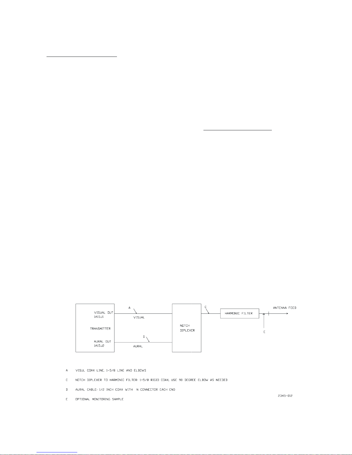
RF System Layout
The 1 5/8 EIA unflanged visual RF output and the N connector
aural output areon the top of thecabinet. Adapters arefurnished
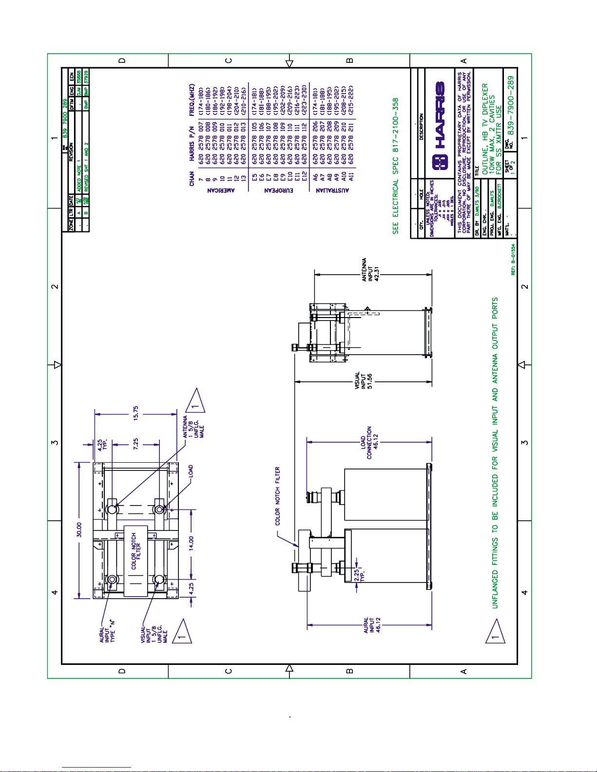
where needed to connect RF coax cables to 1 5/8 EIA components. The outline drawings of typical RF notch diplexers and
harmonic filters are included. Use the block diagrams and
component outline drawings (Fig 2-2 through 2-11) to plan the
installation for the site requirements. Locate the transmitter
close to thediplexerto minimize theinterconnectionline losses.
A support system should beinstalled sothat the RF components
are completely supported,to minimizethe weight carried by the
Section II
Installation
output connectors. This will prevent possible damage to components and connectors. Notch diplexersare generally supplied
in a frame which rests on or is bolted to the floor.
Directional couplers for metering are in the transmitter cabinet.
Optional directional couplers for monitoring are on the block
diagram and should be ordered with the transmitter. Be sure all
components necessary for installation are available on site.
2.2.4
Air System
Minimum transmitter air cooling requirements are 1200 cubic
feet per minute (34 cubic meters per minute). Additional flushing air is recommended for the removal of heat from any
equipment surrounding the transmitter. A good guideline is to
keepinputair no greater than 5°C above ambient. The maximum
transmitter operating temperature is 45°Catsealevel(derate
2°C for each 1000 feet (300 meters) above sea level. Hot air
rises, one approach would be to use exhaust duct(s) or louvers
at the highest point of the room and use a supply fan and filter
frame to keep the room at a positive pressure.
Appendix B contains information useful to those intending to
use air conditioning equipment to control transmitter building
temperature.
2.3 Electrical Installation Planning
Each country establishes standards for AC power systems. The
national and localapplicable standard for the installationshould
be followed.
See Appendix C for information about lightning and surge
protection.
2.3.1
Power Requirements
The transmitter is designed to operate from 208 to 240 volts,50
or 60 Hz, single phase. If voltage variations in excess of
areanticipated, it isrecommended that thetransmitter ACmains
be equipped with automatic voltage regulators capable of correcting the primary voltage.
All control wiring and signal inputs are located at the I/O panel
in the cabinet. Additional access is provided in the cabinet floor
for AC wiring only. AC power to the transmitter should be run
in metallic conduit, connected to earth ground for safety and to
provide shielding against interference. The power wiring must
be terminated in a power distribution panel,this panelmust also
beconnected to earth ground.Atransmitter cabinet ground strap
connection is located at the lower rear edge.
2.3.2
Circuit Breaker Selection
The transmitter requires a relatively stable source of input
power. For this reason, the primary power for the transmitter
should originate at the main power distribution system and
remain isolated from other electrical distributions.
+10%
WARNING: Disconnect primary power prior to servicing.
888-2457-001 2-1
Page 20

Platinum™ Series
Table 2-1. Recommended Test Equipment
Ve stigial Sideband Demodulator Tektronix 1450/1350 or
Equivalent
Option 1 37 MHz IF, NTSC CCIR-M (USA and others)
Option 2 38.9 MHz IF, CCIR-G, PAL
Tektronix Sideband Analyzer
Consisting of:
1405 Sideband Adaptor
2710, 490, or 2750 Spectrum Analyzer
Tektronix 1910 Signal Generator or equivalent
Tektronix 1780 Video Measurement Set
Aural Stereo Generator, Orban 8182A or equivalent
Aural Demodulator Tektronix 751, TFT-850,or equivalent for
stereo
Time & Frequency Technology 701, 702, or equivalent for
monaural
A method of measuring transmitter frequency with two
sources. (Frequency Counter, Frequency Counter on Demodulator, Outside Frequency Measuring Service.)
Audio Oscillatorand Distortion Analyzer (Sound Technology
1710A or equivalent).
Asaca 201-1 Envelope Delay Measuring Set
Scope Camera
RF Bridge, Ealge RLB-150, or precision directional coupler
700-1289-000
UHF RF Notch Filter, Eagle Model TNF-1 484-0300-000
Various RF Adaptors and Connectors
3-1/8 inch to type “N” adapter - 620-0008-000
Type N to BNC male to female - 620-0128-000
Type N to BNC female to male - 620-0547-000
Type BNC plug to Subminiax Plug
Type BNC plug to Subminiax Jack
Type BNC barrel - 620-0604-000
Type BNC to SMB (push-on) - 620-0628-000
TNC-BNC - 620-2821-000
Bird Model 43 Wattmeter with elements from 1W to 1000W
Adaptor 1 5/8" coax to N connector
Manometer Dwyer model40-1 (range 0.1-0-1.0"WC)or equal
Tee kit Dwyer A-604T or equal
Fluke Multimeter and Style C Current Probe
A short-duration surge, due to transformer inrush current, will
occur at turn-on or during a short AC power loss.This surgecan
be as high as 400 amps. During this surge,the linevoltage at the
cabinetmustnotdropbelow80%of the rated line voltage. Select
a 40 amp breaker or fuse for the transmitter using the above
inrush current information.
AC mains Disconnect Location
2.3.3
The circuit breaker panel should be located near the transmitter
in a well lighted area. As a safety precaution, controls for
disconnecting the main power service supplying the transmitter
must be convenient to the operator and maintenance personnel.
Breakers must be clearly labeled. Provisions for emergency
lighting should be made.
2.4 Unloading and Unpacking
2.4.1 Equipment Required for Unloading
Examine the weights listed on the Transmitter Outline drawing
for guidance on the equipment needed. Note: The notch
diplexer, if used, will be the heaviest.
Unpacking, Equipment Inventory and Inspection
2.4.2
A“check-off”boxis availableto help the installertrackthe steps
that have been completed.
Whenthetransmitteris deliveredtothesite, the shipment should
be inspected and inventoried before installation is begun. This
section provides information to assist unpacking and inventory.
Locate the packing check list when the shipment arrives.
Each transmitter shipment will be accompanied by a packing
check list identifying which equipment is packed in the various
crates and boxes.
LOCATED PACKING CHECK LIST
The contents of the shipment should be inventoried with the
packing list. Carefully unpack the unit and perform a visual
inspection to determine if any apparent damage has been incurred during shipment. Retain all shipping materials until ithas
been determined that all items on the list are on site and no
damageoccurred during shipment.It maybenecessaryto search
packing material for parts initially missed during unpacking.
The carrier may also wish to examine the packing material.
If the contents are incomplete, or if the unit is damaged electrically or mechanically, notify the Harris Customer Service Department by phone at 217-222-8200, FAX at 217-222-9443 or
at the following address:
Harris Corporation,
Broadcast Division
P.O. Box 4290
Quincy, Il 62305
Attn. Customer Service Department
INVENTORY OF EQUIPMENT COMPLETED
The equipment becomesthe propertyof the customer when the
unit is delivered to the carrier. Claims for damaged equipment
2-2 888-2457-001
WARNING: Disconnect primary power prior to servicing.
Page 21
Section II - Installation
must be filed promptly; otherwise, the carrier may not accept
the claim.
2.4.3
Factory Test Data Sheets
Factory test data is supplied with each transmitter. It lists parameters for operation of the transmitter. These readings were
recorded during factory testing. Locate the test data and place it
in the manual at the end of the maintenance section.
Record the same readings periodically to establish and maintain
an information base from which to work in the event of future
changes or problems.
FACTORY TEST DATA LOCATED
Cabinet Placement and Leveling
2.4.4
Four bolts hold the cabinet to its skid. They are located two per
side, front and rear. When the cabinetis inits final position, you
may need to level the cabinet. The HT EL cabinet has leveling
jacks in the corners to aid in leveling the cabinet on un-even
floors.The four 0.5inch hold-downs in thebottomofthe cabinet
used to bolt the cabinet to the shipping skid that may be used to
bolt the unit to thefloor.Levelthecabinet using shimsunder the
bottom, this is important to avoid deforming the cabinet when
bolting it to the floor.
Install the power module assembly in the bottom of the rack. It
will slide intomating electrical connectors.Install the Exciter(s)
and connect power and signal cables to exciter(s).
NOTE
DO NOT INSTALL RF MODULES AT THIS TIME
WARNING: Disconnect primary power prior to servicing.
Figure 2-1. Transformer Taps
888-2457-001 2-3
Page 22

Platinum™ Series
2.5.2
2.5 Electrical Installation
2.5.1 Grounding
Located in the lower left rear corner of the cabinet is a ground
strap. Connect thestation groundto this strap with 2 inch(5 cm)
copper strap. For additional information on station grounding
requirements refer to Appendix C.
GROUND STRAP CONNECTED
Table 2-2. Input Signals & Remote Conrol I/O
SYMBOL FUNCTION CONNECTOR LABEL CONNECTOR TYPE
Exciter A Exciter B
J1 J11 Video Input VIDEO IN BNC
J2 J12 Aural Composite input COMP AUR BNC
J3 J13 Aural Subcarrier 1 AUR SCA 1 BNC
J4 J14 Aural Subcarrier 2 AUR SCA 2 BNC
J5 J15 Precise Frequency Control Input PFC IN BNC
J6 J16 Monaural Aural Input/Dual Sound Audio 1 MONO AUR 1 XLR
J7 J17 Monaural Aural Input/Dual Sound Audio 2 MONO AUR 2 XLR
J8 J18 NICAM Reference BNC
J9 J19 NICAM IF In BNC
J10 J20 Option Access BNC
J21 Remote Command Input 37 Pin D
J22 Remote Status Output 37 Pin D
J23 Remote Analog Output 37 Pin D
Primary Wiring
(Refer to drawing 839-7994-179.)
AC power is connected to terminal block 1A14TB1 located on
the right wall inside the rear door. Use #8 A WG wire at a
minimum or larger if required by Wiring Codes. Connect the
“hot” side of the ac line to 1A14TB1-1, the neutral side to
1A14TB1-2 and connect 1A14TB1-3 tothe safety or protective
ground wire.
PRIMARY WIRING CONNECTED
Table 2-3. Setup Jumpers - Normal Positions
1A2 Exciter Meter/Control Board
JP # POSITION FUNCTION (AS SHIPPED)
JP1 1-2 Loss of video enabled
JP2 1-2 Remote control of aural group delay
JP3 1-2 Remote control of notch diplexor
1A3 Interface Logic
JP# POSITION NORMAL FUNCTION
JP1 1-2 Visual foldback enabled
JP2 1-2 Aural foldback enabled
JP3 1-2 Aural AGC enabled
JP4 1-2 Source/Sink for Remote Status
JP5 1-2 Source/Sink for Remote Command
JP6 Factory Select Aural AGC 2dB pad select
JP7 1-2 Exciter A fault select DIGITAL
JP8 1-2 Exciter B fault select DIGITAL
JP9 1-2 Power supply 3 not present
JP10 1-2 Video control enabled
JP11 Factory Select Aural AGC 3dB pad select
JP12 1-2 Aural AGC enabled
JP13 Factory Select Visual AGC 3dB pad select
JP14 Factory Select Visual AGC 2dB pad select
JP15 1-2 NO 5 sec restart, AC FAIL
JP16 1-2 High VSWR shutdown enabled
2-4 888-2457-001
WARNING: Disconnect primary power prior to servicing.
Page 23

Section II - Installation
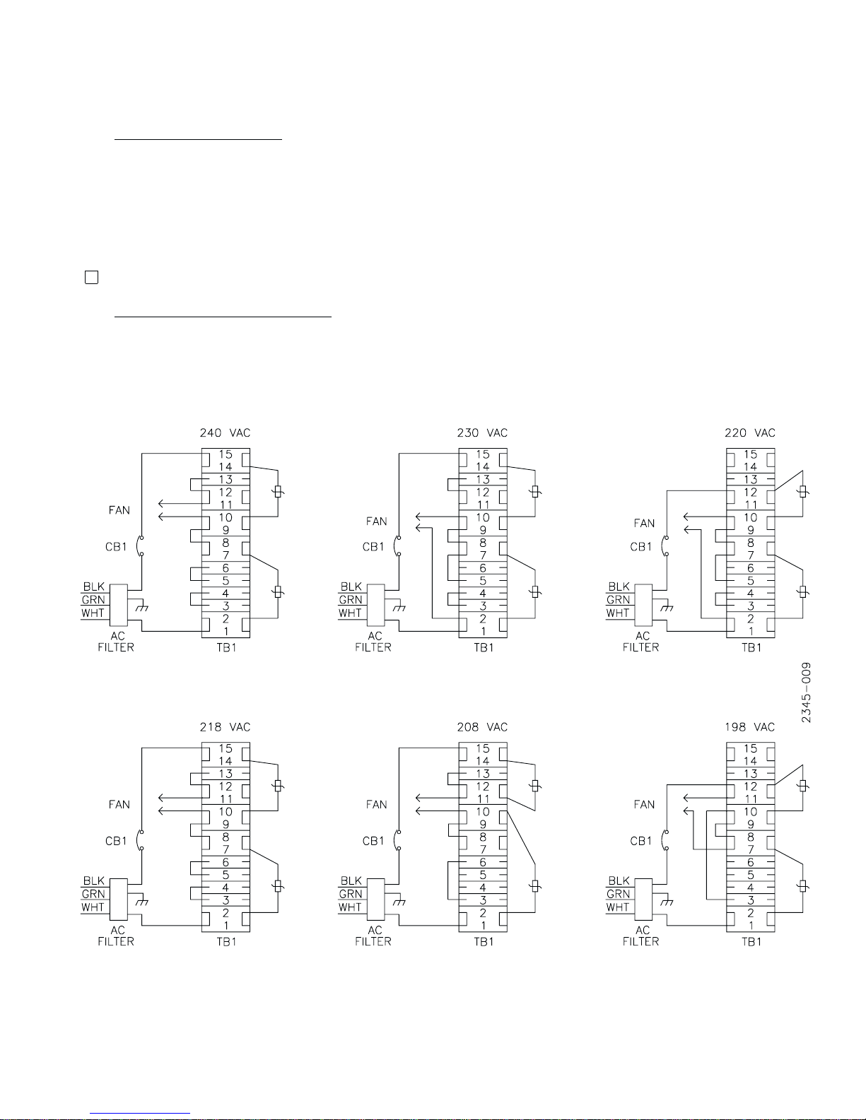
2.5.3 Setting Transformers Taps
Check taps on the power supply in the exciter. Refer to figure
2-1, or drawing 839-7900-504. The logic supply 1A11PS1
located in the rear of the power module behind the 1A12 I/O
panel is tapped as shown in chart below
PRIMARY VOLTAGE
208-220 230-240
JUMPER CONNECTION 2 AND 3 2 AND 3
AC CONNECTION 1 AND 5 1 AND 4
TRANSFORMER PRIMARY TAPS CHECKED
Input Signals
2.5.4
The input signals and remote control I/O are located on 1A12.
See Table 2-2.
NOTE: The coax wiring for the External Precise Frequency
Control (PFC) option is installed in the cabinet. If the PFC
option is purchased the wiring will be added to the exciter.
INPUT SIGNALS CONNECTED
Setup Jumpers
2.5.5
Check the set-up jumpers, located in the exciter 1A2 and Interface Logic 1A3. Jumpersare normally shipped from the factory
in the positions shown in Table 2-2. They may be changed if
needed.
JUMPERS SET FOR CORRECT CONFIGURATION
Backup Battery
2.5.6
CAUTION
DO NOTUSE RECHARGEABLE BATTERIES
The battery holder will accept three size AA (NEDA 15A) 1.5
Volt batteries. These batteries furnish power to hold the transmitter status in the control system and control the return to
operation when AC power returns. The batteries should be
replaced as part of a regular mantenance schedule.
2.5.7
RF Output Coax Connections
(Refer to 843-5285-110)
The RF output connections, 1A15J1 for visual and 1A15J2 for
aural are located on the top of the cabinet. Make any desired
VSWR measurements of the RF plant before making final
connections to the cabinets.
2.5.8
Interlocks
External interlocks are connected to REMOTE COMMAND
1A12J21-7. A contact closure to ground mustbe present to turn
on the transmitter. If this interlock is not used, 1A12J21-7 must
be jumpered to ground.
The external contact closure or other device must sink 50
microamps to less than 0.5 volts. Open circuit voltage is +5V.
INTERLOCK WIRING INSTALLED
2.6 Transmitter Check Out
2.6.1 Pre-turn on checks
CAUTION
BEFORE PROCEEDING WITH CHECK OUT, INSPECT THE
TRANSMITTER FOR AC POWER SHORTS, LOOSE HARDWARE,
WIRINGERRORS,UNCONNECTEDWIRES, MISSING PARTS,AND
DEBRIS.
2.6.2 Initial Turn-on Sequence
The following procedures arethe sequential stepsto safely turn
on the transmitter, and must be performed in the order listed. It
is recommended that the installation personnel read the general
description in section one, the controls and operation material
in section three, and these procedures before starting.
a.
MODULESMUST NOTBEINSTALLEDAT THIS TIME
b.
Apply 1 volt p-p video to exciter video input.
c.
Theloss of video indicatorshould extinguish immediately
or after the loss of video times out depending on option
that is jumper selected.
d.
Press transmitter ON pushbutton.
e.
Openthe externalinterlock. The external interlock lampshould
be illuminated and the transmitter should shut off. Press ON
button.The transmitter shouldnot come on.Closethe interlock
circuit. The external interlock lamp should extinguish.
f.
Verify operation of RAISE and LOWER switches.
g.
If the system has a remote control, place transmitter in the
REMOTE mode and check for operation of transmitter
ON/OFF and RAISE/LOWER from the remote.
h.
Verify that LOCAL mode inhibits remote commands.
i.
Return exciter to minimum power by depressing and
holding LOWER commands for about 15 seconds.
j.
Measure the 50 voltsupply by usingthe multimeter onthe
front of the exciter. It should measure 50 volts.
k.
Press transmitter OFF pushbutton.
2.6.3
Module Installation
The modules may now be installed. Refer to factory test data for
placement ofmodules byserial number and slotnumber.There are
threetypesofmodules,DRIVERS, HIGHPOWERDRIVERS and
PA’s. The DRIVERS are keyed to be eitherstandard or high power
drivers and will not fit into a P Aslot. Use of a P Ain a driv eslot is
for emergency only. Although each type is interchangeable from
aural to visual and will work in any like socket, when starting out
it is best to reassemble them in the same locations as tested. Keep
a record of any changes for future reference.
Make sure each module is completely seated.
CAUTION
DO NOT USE EXCESSIVE FORCE INSTALLING MODULES INTO
THE SLOTS.
WARNING: Disconnect primary power prior to servicing.
888-2457-001 2-5
Page 24

Platinum™ Series
2.6.4 Control System Check Out
a.
Depress andhold powerLOWER controls for 15 seconds
each to ensure that exciters are turned all the way down.
b.
Press transmitter ON pushbutton.
c.
Check that all modules are enabled. Drivers will show a
full green LED. PA modules will illuminate half of the
green LED. It is normal for the red module LEDs to come
on momentarily as the transmitter 50 volt supplies come
up to voltage at turn on. They also will come on at
shut-down,gradually fading outas the suppliesdischarge.
d.
Open back door and verify that all fans are functioning.
e.
Check MODULE FAULT status for each module. Check
to see that all modules are enabled (green LED on); press
transmitter ON to enable any modules that are not already
on.
f.
Squeeze the disable switch in the handle of the first
module. The module LEDsshould go out. You should see
the MODULE FAULT lamp on at the control panel. Reenable the module by pressing transmitter ON at the
control panel. The MODULE FAULT lamp on the control
panel should go out. Repeat procedure for each module.
2.6.5
Initial Application of RF Power
2.6.5.1 Visual
a.
LOWER the exciter to minimum drive and apply a ramp
or staircase test signal.
b.
Press transmitter ON pushbutton.
c.
Check to see that all RF amplifier modules are enabled.
d.
Slowly raise visual power while observing VSWR and
FORWARD POWER. Stop at approximately 25% forward power .
e.
Switch video to black picture with no setup for power
calibration. Sync peak power multiplied by a system
dependantconstantequalsaveragepower.Some constants
are 0.568 (CCIR B) and 0.595 (CCIR M)
f.
Using an external power meter to confirm power output,
slowly increase visual power to 100% on external power
meter.
If external power meter and panel readings do not reasonably agree, refer to the power calibration procedures
in Section 5.
g.
Atfulloperatingpowermeasurethebelowparametersand
adjust if needed. See Section 5 for alignment procedures.
Depth of modulation
Differential gain
Incidental phase (ICPM)
Differential phase
Amplitude response and group delay compensation
(Exciter Group Delay Compensator and Notch Diplexer
Equalizer adjustments)
Power limit
Frequency
2.6.6
Aural
a.
Slowly apply aural exciter drive while watching VSWR
and FORWARD power. If a notch diplexer or hybrid
output combiner is used, check its reject load power as
well. Stop at about 50% and use external power metering
to confirm power.
b.
Check the AURAL FWD readings against the external
meter. Refer to power calibration in Section 5 if needed.
c.
Apply aural baseband signals to the appropriate exciter
input(s). Adjust the input level(s) using Section 5 as a
guide for correct deviation.
d.
CompareDC INPUTPOWERand50 voltsupplycurrentto
factory test data at no signal and black picture conditions.
2.7 Remote Control Input and Output
Command In 1A12J21
Status Out 1A12J22
Analog Out 1A12J23
2.7.1
Command In 1A12J21
The Command inputs are optocoupled and mustbe asserted low
to turn on the function. The optocoupler is supplied by the +12
volt supply and require a current sink of 5 ma to activate the
input.
Command Functions:
PIN FUNCTION
1 Transmitter ON
2 Transmitter OFF
3 Visual raise power
4 Visual lower power
5 Aural raise power
6 Aural lower power
7 External interlock
8Spare
9 Loss of video over-ride
10 Exciter comp/mono select
11 Aural group delay select
12 Notch diplexer select
13 Exciter switcher auto select (option)
14 Exciter switcher manual select (option)
15 Exciter switcher a exciter select (option)
16 Exciter switcher b exciter select (option)
17-19 Not used
20 Common (+12V or gnd JP-4 & 5 option)
36-37 Not used
2.7.2
1A12J22: Status Outputs
The Status outputs are open-collector drivers with a 100 Ohm
resistor in series and a 24 volt zener (avalanche)diode clamp to
ground. An internal voltage source of +12 volts can be made
available to the outputs by placing main controller optional
status jumper J21 in the 1-2 position. When in the 2-3 position,
an external voltage source must be supplied. Theopen collector
2-6 888-2457-001
WARNING: Disconnect primary power prior to servicing.
Page 25
Section II - Installation
is30 volts DCmaximum, and maximumcurrentmust be limited
to 48 Ma. Each output is asserted low for status true condition.
2.7.3
Status Functions 1A12J22
PIN FUNCTION
1-16 Common (+12V or gnd JP-4 & 5 opt)
17-19 Not used
20 Transmitter ON status
21 Local status
22 Loss of video status
23 Frequency unlock status
24 Corrector bypass status
25 RF muted status
26 Air fault status
27 High vswr status
28 Foldback active status
29 Module fault status
30 50 volt power supply fault status
31 External interlock status
32 Exciter switcher auto selected (option)
33 Exciter switcher manual selected (option)
34 Exciter switcher A selected (option)
35 Exciter switcher B selected (option)
36 No connection
37 No connection
LOCAL: Indicates the transmitter will not accept remote command inputs. This line will be asserted low when the transmitter
is in the LOCAL mode.
VSWR FOLDBACK ACTIVE: Indicates antenna VSWR has
caused the transmitter to reduce its output power. It will be
asserted low while the foldback is active.
HIGH VSWR(VSWR FAULT): Indicates the modules have not
come up to power at the end of three seconds after a VSWR
overloadset point has beenexceeded. Note thatactivefold-back
will inhibit VSWR overload detection. Upon detection of an
overload, this line will be asserted low.
EXTERNAL INTERLOCK: Indicates the status of the external
interlock. If the interlock is open, a low will be asserted.
RF MUTE: Exciter mute: Indicates that some function has
muted the exciter. Asserted low for mute.
EXCITER FAULT: Indicates exciter fault directly in single
exciter configuration. Asserted low for fault.
SUPPLY FAULT:Indicates the 50 volt powersupply has failed.
Asserted low upon fault.
MODULE FAULT: Indicates one or more of the cabinet RF
modules has faulted off. Asserted low upon fault.
AIR LOSS: Indicates a loss of air flow. Asserted low upon loss
of air flow.
SPARE FAULT: Not used at this time.
2.7.4
Analog Outputs 1A12J23
The analog outputs on the I/O panel provide bothcalibrated and
un-calibrated readings for some functions. The calibrated outputs are a function of the monitoring system. The raw outputs
come directly from the RF peak detectors. Each output is buffered by avoltage follower,with a1 k Ohm resistor inseries with
the signal, before leaving the main controller board.
PIN FUNCTION
1 Visual forward power
2 Visual reflected power
3 Aural forward power
4 Aural reflected power
5 50 volt power supply voltage sample
6 50 volt power supply current sample
7 +5 volt logic supply voltage sample
8 +12 volt logic supply voltage sample
9 -12 volt logic supply voltage sample
10 Inlet temperature
11-14 Not used
15 Exciter status: A Failed
16 Exciter Status: B Failed
17-19 No connection
20-35 COMMON
36-37 No connection
WARNING: Disconnect primary power prior to servicing.
Figure 2-2.
888-2457-001 2-7
Page 26
Platinum™ Series
2-8 888-2457-001
WARNING: Disconnect primary power prior to servicing.
Figure 2-3.
Page 27
Section II - Installation
WARNING: Disconnect primary power prior to servicing.
Figure 2-4.
888-2457-001 2-9
Page 28

Platinum™ Series
2-10 888-2457-001
WARNING: Disconnect primary power prior to servicing.
Figure 2-5.
Page 29

Section II - Installation
WARNING: Disconnect primary power prior to servicing.
Figure 2-6.
888-2457-001 2-11
Page 30

Platinum™ Series
2-12 888-2457-001
WARNING: Disconnect primary power prior to servicing.
Figure 2-7.
Page 31

Section II - Installation
WARNING: Disconnect primary power prior to servicing.
Figure 2-8.
888-2457-001 2-13
Page 32

Platinum™ Series
2-14 888-2457-001
WARNING: Disconnect primary power prior to servicing.
Figure 2-9.
Page 33

Section II - Installation
WARNING: Disconnect primary power prior to servicing.
Figure 2-10.
888-2457-001 2-15
Page 34

Platinum™ Series
2-16 888-2457-001
WARNING: Disconnect primary power prior to servicing.
Figure 2-11.
Page 35

3.1 Introduction
This section identifiesall controlsand indicatorsassociated with
the Platinum™ Series HT EL Transmitter. The exciter control
panel contains the operator controls, indicators and metering for
the transmitter. The Interface Logic Module has additional indicators for power supply status and reflected RF power foldback.
3.2 Controls And Indicators
Refer to Figure3-1 for the location of all controls and indicators
associated with day-to-day standard operation of the transmitter.
The function of each control and indicator is listed in Table 3-1.
Interface Logic Module 1A3 LED indicators
INDICATOR FUNCTION
+5 VOLT Indicates the 5 volt logic supply is on
+12 VOLT Indicates the +12 volt supply is on
-12 VOLT Indicates the -12 volt supply is on
+50 VOLT Indicates the 50 volt supply is on
VIS F/B ACT Indicates reflected visual RF power is
causing the visual power to foldback
AUR F/B ACT Indicates reflected aural RF power is
causing the aural power to foldback
Section III
Operation
Next select visual output power (VIS FWD) on the multimeter
and press visual raise “up arrow” or visual lower “down arrow”
button to set the visual poweroutput level.
Next select aural output power (AUR FWD) on the multimeter
and press aural raise “up arrow” or lower “down arrow” to set
the power output level. If the transmitter is to be operated by
remote control press REMOTE button to enable the command
remote control inputs.
To turn transmitter off, push the OFF button.
3.4 Video Controlled Operation
If the loss of video jumper 1A3JP1 is in the 1-2 position and the
over-ridejumper on 1A2JP1 is in NORMAL position the loss of
video detector is enabled. This provides two user adjustable
delaysone for videopresentand the other videolossdelay.When
video is applied, the video present delay timer will holdoff turn
on of the transmitter until the present delay times out. On loss of
video,the transmitterwill change to a predetermined (adjustable)
cw power level until the loss timer has timed out, then automatically turn transmitter off.
3.3 Local Turn-on and Turn-off
The control panel on the front of the exciter contains all the
operator controls and fault indicators. To turn the transmitter on
first apply a video signal to the video input. After the VIDEO
LOSS indicator turnsoff,pressing the transmitterON button will
place the transmitter on air.
3.5 Remote Control/Extended Operation
Verify that the HT EL is not in local operation mode. The
transmitter can the be operated by following the instructions for
the control system in use.
If the transmitter fails to operate begin analyses by checking the
status of the indicator LED’s on the control panel. Refer troubleshooting and repair to qualified technical personnel. Theory
of operationand othertroubleshooting informationare inappropriate sections of the manual.
WARNING: Disconnect primary power prior to servicing.
888-2457-001 3-1
Page 36

Platinum™ Series
Figure 3-1. Transmitter Controls and Indicators
3-2 888-2457-001
WARNING: Disconnect primary power prior to servicing.
Page 37

Section III - Operation
Table 3-2. Transmitter Controls and Indicators
Ref. Item Function
1 Multimeter VisualForward Power in Watts
VisualReflected Power in Watts
Sound Forward Power in Watts
Sound 2 Forward Power in Watts
Sound Reflected Power in Watts
Module Power Supply in Volts
Module Current in Amps
Exciter Visual Power in Watts
Exciter Video Input Level in mV
Exciter Sync Input Level in mV
Exciter Sound 1 Power in mW
Exciter Sound 2 Power in mW
Exciter Sound Deviation in kHz
Exciter Audio Input Levelin mV
2 Selection Indicates Multimeter reading selection
3 Bar Graph Indicates Multimeter 0000 to 1000
4
5
↑
↓
Multimeter selector button roll-down
Multimeter selector button roll-up
6 Xmtr ON Turn TransmitterON
7 ON Indicator Lights when Transmitter is ON
8 Xmtr OFF Turn Transmitter OFF
9 LOCAL Inhibit Transmitter remote control inputs
10 LOCAL Indicator Lights when in LOCAL only mode
11 REMOTE Enable Transmitter remote control inputs
12 Remote Indicator Lights when in REMOTE mode
13
14
15
16
↑
↓
↑
↓
Raise Visual Power of Transmitter
Lower Visual Power of Transmitter
Raise Aural Power of Transmitter
LowerAuralPowerofTransmitter
17 POWER When ON, indicates A Cpower to Exciter
18 EXTERNAL INTERLOCK When ON, indicates external interlock OPEN
19 50V SUPPLY FAULT When ON, indicates power supply fault condition
20 MODULE FAULT When ON, indicates one or more of the modules has a fault condition
21 AIR FAULT When ON, indicates loss of air
22 HIGH VSWR When ON, indicates a high VSWR condition
24 RF MUTED When ON, indicates RF Output of Exciter is muted
25 CORRECTOR BYPASS When ON, indicates one or more corrector boards in the BYPASS mode
26 FREQUENCY UNLOCK When ON, indicates one or more of the phase lock loops are unlocked
27 VIDEO LOSS When ON, indicates a loss of input video or video preset delay
28 VISUAL F/B ACT Indicates a VSWR is causing the visual & aural power to foldback
29 AUTAL F/B ACT Indicates a VSWR is causing the aural power to foldback
30 50 VOLT POWER Indicates the 50 volt supply is on
31 5 VOLT POWER Indicates the 5 volt logic supply is on
32 +12 VOLT POWER Indicates the +12 volt supply is on
33 -12 VOLT POWER Indicates the -12 volt supply is on
34 PRE-CORRECTED VISION IF Corrector output
35 VISION IF MODULATOR IF Modulator Output
36 PRE-CORRECTED VIDEO Modulator Input Video
WARNING: Disconnect primary power prior to servicing.
888-2457-001 3-3
Page 38

This page left blank intentionally
Page 39

Section IV
Theory of Operation
4.1 Introduction
This section provides theory of operation for the HT EL 2000
TV Transmitter. For purposes of discussion, the circuitry is
dividedintofunctionalsubassembliesinthefollowingtext.Refer
to the separately packaged diagrams as required.
4.2 System Overview
The transmitter is composed of subassemblies mounted in a
common cabinet. The 1 watt visual and aural signals are generated in a exciter chassis with exciter powermetering andcontrol.
The exciter front panel and the Interface Logic Module implement transmitter metering and transmitter control.
Modulated visual RF signal is amplified in a DriverModule and
divided four ways. Three outputs drive visual Power Amplifiers
(PA’s), the other is terminated in a load. The three PA’sare
combined in a three way Gysel combiner. The Gysel combiner
features a constant 50 ohm input and a high degree of isolation
between modules. This allows removal of one module without
impacting the others. The output forward and reflected power is
sampled bythe transmitter for meter reading andVSWR protection.
Auraldrivefrom the exciter isamplifiedbya drivermodule. This
aural RF signal is also sampled for metering and VSWR protection.
Thepowersupplies consist oftwohigh power switching supplies
connected in parallel for the RF modules and a small supply for
the interface logic.
The optional Exciter Switcher contain level sensing circuitry,
logic and transfer relays for automatic exciter switching.
4.3 Exciter, Meter and Control Board
The meter board is mounted to the back side of the exciter front
panel and provides the metering, control and status indications
for the transmitter.
4.3.1
A/D & Displays
Schematic drawing 839-7994-125 shows the meter board for the
transmitterwith sheetone being the analogmeteringsection.The
meter is a digital 4-1/2 digit A/D convertor with multiplexed
binary coded decimal(BCD) outputs. Thisis followed bya BCD
to seven segment display decoder and LED displays.
TheA/D U1 can display0000to 9999 on thedigital displaysDS1
and DS2 and is updated about 5 times a second. The display is
normally calibrated for 2000 when the Bar Graph is at full scale
or 1.25 volts at pin 5 of U2 and U3 Bar Graph display ICs.
The A/D referenceadjust isset for 1.000 volts between pin2 and
ground. Each metering input has a calibration control.
4.3.2
Bar Graph Display
The Bar Graph displays consisting of U2 and U3 are designed
using LM3914s cascaded to make a 20 bar magnitude display
which lights all 20 bars with 1.25 volts applied to pin 5. Each
meter position also has a corresponding calibration adjustment
for the analog bar display.
4.3.3
Analog Multiplexers
The analog multiplexer consisting of U4 and U6 provides the
analog selection switches to apply the various voltage monitor
points the A/D and Bar Graph displays. IC U4 is an 8 channel
multiplexerandisused to route thepowersamplepointsto buffer
U7 and on to U5 an analog squaring circuit. The squared sample
is then passed through U6-1 to 2 and on to the display circuits.
The two linear voltage samples, 50V and supply current, are
routed through U6-4 to 3 or U6-8 to 9 to the displays.
ENABLE
ADR U4 U6 DESCRIPTION
0 4-8 1-2 VISUAL FORWARD POWER
1 5-8 1-2 AURAL FORWARD POWER
2 6-8 1-2 VISUAL REFLECTED POWER
3 7-8 1-2 AURAL REFLECTED POWER
4 12-8 1-2 EXCITER VISUAL OUTPUT POWER
5 1-8 1-2 EXCITER AURAL OUTPUT POWER
6 x 4-3 50 VOLTS SUPPLY
7 x 8-9 MODULE CURRENTS
Rev. B: 7/15/02 888-2457-001 4-1
WARNING: Disconnect primary power prior to servicing.
4.3.4
Meter Selector
The multiplexers are controlled from the meter selection PAL
U17 on sheet 4 of the schematic. This PAL contains a three bit
up/down counter plusdecoders to enablethe multiplexersfor the
Table 4-1. Meter Counter/Display Function
Page 40

Platinum™ Series
sample selected and the decimal point selection for the digital
display. The enable line (EN_SQ, EN_VOLT, EN_CUR) to the
multiplexersis assertedHI andthe decimal points (DP1*, DP2*,
DP3*) are asserted low to turn on the display decimal point.
NOTE: The (*) character is used to denote a signal is asserted
LOW when true.
Table 4-1 shows the address of A0, A1, & A3 (ADR) the three
bit meter selection counter coupled to the functions displayed.
Loss Of Video Delay Detector
4.3.5
The Loss of Video Delay Detector, page two, is made up of U8
through U14 to form a function “on” video present delay of 3.5
to9.2secondsandonvideolossadelayof1to2.7minutes.The
function can be inhibited by placing JP1 in the 2-3 position or
enabled in the 1-2 position.
With JP1 in the NORMAL (1-2) position and video present the
reset to U11-6 is asserted low allowing the oscillator in U11 to
run startinga terminalcount of 32768. This will assert U11-8 Hi
which clocksU13-3 (D latch) Hi causing U13-5 to change to the
state of the D input which is Hi. This will assert U13-6 low
causing U14-1 to assert Hi signaling the delayed presence of
video and un-mute the rf mute circuit.
On the loss of video U11-6 is asserted Hi resetting the video
present counter and U12-6 is asserted low allowing U12 to start
counting. At the time between loss of video and the terminal
count of U12 the visual rf level is reduced by asserting U16-18
low which inserts R41 CW LEVEL SET pot in the visual power
control circuit. At the terminal count of 32768 U12-8 will assert
Hi causing U14-10 to assert low causing U13-1 to reset the D
latch asserting U13-6 Hi causing U14-1 low signaling the delayed loss of video which will rf mute exciter output.
Oscillator U22 is running about 77.6kHz and is programmedfor
a divide by 256 to produce the 300Hz output frequency.
BATTERY (BAT) SUPPLY VOLTAGE
4.3.8
All the PALs operate from the BAT Vcc supply line which
maintains voltage on the counters in the event of a power failure.
At some point after that all counters will be reset to 0 on power
return if BAT drops to a low enough voltage. BAT is supplied by
three AA size batteries mounted on the rear of the exciter.
Visual Power Control
4.3.9
The visual power control is shown on sheet 5 of the schematic
and controls the rf output of the visual channel. The 12 bit
up/down counter consists of U26& U27which supplies a binary
code to the DAC U25 which controls the gain of U24-1
VIS_DAC_BUF. Thesignal is passed through the rf muteswitch
U23-1to2andontoU23-3to4CWLEVELSETswitchandon
to U24-5 VIS_CTRL_BUF subtractor circuit where the visual
reflected power foldback input reducesthe output when applied.
VIS_PWR_CTRL J1-23 will normally swing between 0 and 4
volts for a 0 to 1 watt output level but can vary somewhat and
will depend on where R48 VIS_PWR_LIMIT is set.
4.3.10
Theaural power control shownon sheet6of the schematic works
the same as the visual except there is no CW_LEVEL_SET
switch in the aural path.
4.3.11
The power up resetcircuit is U31 which forms a voltage comparator referenced to the 1.23 volts of CR11, normal power fail
detection point is about 4.6 volts. When the voltage of U31-3 is
morethan U31-2 thenU31-1 will assertaHi removing the power
up reset signal.
Aural Power Control
Power Up Reset
4.3.6
Override/Normal Selection
Located in the upper right hand corner of the meter board is JP1
NORMAL/OVERRIDE jumper selection. In the NORMAL position the delay timers operate as outlined above. In the OVERRIDE position both delay timers are inhibited and the loss of
video signal is passed through U14 to rf mute circuit of the
exciter.
Clock Circuits
4.3.7
Sheet 4 of the schematic shows the clock PALs for the up/down
counters for VISUAL RAISE/LOWER U18, AURAL
RAISE/LOWER U19, METER CLOCK U20, and METER SELECT U17. U18 and U19 are clocked by the 300Hz oscillator
U22 to generate the VIS_PWR_CLK and the AUR_PWR_CLK
signals to drive the visual and aural up/down 12 bit counters.
Upon pressing an UP or DOWN button, U18 or U19 pin 23
PWR_CLK willissue onepulse thenwait for2 seconds and start
issuing a 300Hz clock rate if the button is still pressed.
IC U18 also generates a 9.5Hz clock used by the METER
CLOCK GATE U20 which operates similar to U18 & U19 but
at a slower one pulse per 1.17 second rate to clock U17 METER
SELECT 4 bit counter.
4-2 888-2457-001 Rev. B: 7/15/02
WARNING: Disconnect primary power prior to servicing.
4.3.12
These two jumpers extend AUR_GROUP_DELAY and
NOTCH_DIP_ENABLEsignals to the remote control interface.
4.3.13
The unlocked status of the three phased locked oscillator is
displayed by DS27, DS28, & DS29 and passed to PAL U17
where they are combined to produce the signal FREQ_LOCK*
on U17-23. FREQ_LOCK* drives the FREQ UNLOCK status
indicator and the U27-11 where it is combined with
VIDEO_LOSS_DELAY* to generate RF_MUTE U27-22. Also
ifanyFREQUNLOCKorVIDEOLOSSDELAYisassertedlow
the exciter will mute the rf output.
JP2 & JP3
FREQ UNLOCK
Page 41

Section IV - Theory of Operation
4.3.14 VIS_CLK_GATE U18 & AUR_CLK_GATE
U19 Functional Descriptions
IC
PIN TYPE FUNCTION
1 IN CLOCK TO ALL REGISTERED OUTPUTS
2 IN VISUAL POWER UP COMMAND
3 IN VISUAL POWER DOWN COMMAND
4-13 IN NOT USED
14 OUT DIVIDE BY 16 OF CLOCK PIN 1
15 OUT U/D DELAY COUNTER BIT 1
16 OUT U/D DELAY COUNTER BIT 4
17 OUT U/D DELAY COUNTER BIT 0
18 OUT DIVIDE BY 32 OF CLOCK PIN 1
19 OUT U/D DELAY COUNT BIT 3
20 OUT DIVIDE BY 8 OF CLOCK PIN 1
21 OUT DIVIDE BY 4 OF CLOCK PIN 1
22 OUT DIVIDE BY 2 OF CLOCK PIN 1
23 OUT CLOCK TO UP/DOWN POWER CONTROL
PALs U18 & U19 contain a divide by 32 free running counter
plus a gated one-shot delay repeat clock rate counter called U/D
DELAY COUNTER.
The U/D DELAY COUNTER BITS only change state when the
UP or DOWNbutton is pressed otherwise the U/D counter rests
at state 0 count. The U/D counter is clocked once each time pin
18 changes (divide by 32 of pin 1) state. Once the U/D counter
reachesthe count of0Dhit stays thereuntilthe button is released.
Pin 23 POWER CONTROL clocks the 12 bit UP/DOWN
POWER CONTROL counters when the RAISE or LOWER
buttonis pressed. Thefirstone-shot pulse isissuedwhen the U/D
counter is at the count of 04h and then repeats the pin 1 clock
rate after U/D counter reaches the count of 0Dh.
4.3.14.1 METER_CLK_GATE U20 Functional Descriptions
IC
PIN TYPE FUNCTION
1 IN 9.5HZ CLOCK TO ALL REGISTERS
2 IN METER UP COMMAND
3 IN METER DOWN COMMAND
4 IN VISUAL RAISE POWER COMMAND
5 IN VISUAL LOWER POWER COMMAND
6 IN AURAL RAISE POWER COMMAND
7 IN AURAL LOWER POWER COMMAND
8-13 IN NOT USED
14 OUT VISUAL STAY
15 OUT AURAL POWER DOWN
16 OUT VISUAL POWER DOWN
17 OUT VISUAL POWER UP
18 OUT AURAL STAY
19 OUT METER DELAY BIT 2
20 OUT METER DELAY BIT 1
21 OUT METER DELAY BIT 0
22 OUT METER CLOCK
23 OUT AURAL POWER UP
IC U20 contains debounce logic for the raise/lower controls and
the meter up/down plus a 3 bit counter for clocking the meter
select PAL U17. “Debounce” logic is used to change a noisy
switch closure to a defined transition between two logic states.
The 3 bit binary counter divides the 105ms clock on pin 1 by 8
for a 840ms clock rate to U17 METER SELECT PAL when the
meterUPorDOWNbuttonispressed,otherwisethe counter rests
at 0 count.
The RAISE/LOWER COMMANDS are debounced by the
105ms clock and passed on to the POWER UP/DOWN output
pins.
VISUALSTAY output is asserted Hi if neither VISUAL RAISE
or LOWERbuttons are pressed. This signal is used by the visual
power control PALs U26 & U27.
AURAL STAY output is asserted Hi if neither AURAL RAISE
or LOWER buttons are pressed. This signal is used by the aural
power control PALs U29 & U30.
4.3.15
See Table 4-1. U17 Functional Descriptions.
4.3.15.1 VIS_UP/DWN_PWR_CTRL U26 & U27
PALs U26 and U27 form a 12 bit up/down counter with halt
protection at both ends so the count will stop at 0000h 0000h
0000h and FFFFh FFFFh FFFFh which allows a total count of
4096. The counter is reset to 0 on powerup if the BAT supply is
low enough otherwise the count is remembered from the last
setting. The direction of count is controlled by pins 2 & 3
POWER UP/DOWN controls from U20 and the CLOCK is
supplied by U18-23. The RESET input to pin 4 forces a tri-state
mode on power fail condition to disconnect the output pins from
the IC without poweron them. The STAY inputpins 8& 10hold
the counter at the present state unless the raise or lower button is
pressed.
TheVIDEO_LOSS_DELAY*pin 5, FREQ_LOCK*pin11, and
RMT_MUTE pin 13 are combined to form RF_MUTE* on pin
22. Thissignal isasserted lowto mute and is passed to thevisual
and aural rf mute switch U23-13 and U23-12 which opens the
switch causing U24-7 to go to 0 volts.
4.3.16
The visual DAC is placed in the feedback loop of U24-1 to 2
which allows the amplifier gain to be controlled by the binary
number applied to the U25 DAC thereby controlling the output
voltage that U24-1 produces.
4.3.17
The output of U24-1 is passed through U23-1 to 2 RF MUTE
switch and U23-3to 4 CWPOWERLEVEL switch throughR42
to U24-5 VIS_CTRL_BUF where the foldback voltage derived
from the antenna reflected power sample is subtracted from the
visual power level set by the DAC.
4.3.18
The aural power control operates the same as the visual except
thereisnoCWLEVELswitchinthecircuit.
METER_SEL U17 Functional Descriptions
Visual DAC U25
Visual Foldback Control
AUR_UP/DWN_PWR_CTRL U29 & U30
Rev. B: 7/15/02 888-2457-001 4-3
WARNING: Disconnect primary power prior to servicing.
Page 42

Platinum™ Series
4.4 Interface Logic Module
Refer to schematic 839-7994-151.
The Interface Logic Module 1A3 provides the interconnection
and logic to control the RF modules and 50 volt power supply.
Circuitry includes RF power foldback, agc and the rf peak
detectors for forward and reflected power samples.
4.4.1
Peak Detectors
There are four rf peak detectors that convert the rf samples from
the visual and aural directional couplers in to a dc valuefor uses
by the logic.Each rf inputis coupled bya 4:1 step uptransformer
to a HP2800 hot carrier diode detector were the rf is turned into
Table 4-2. U17 Functional Descriptions
IC
PIN TYPE FUNCTION
1 IN 840MS CLOCK TO ALL REGISTERS
2 IN METER UP COMMAND
3 IN METER DOWN COMMAND
4IN RESET
5 IN VISUAL IF OSCILLATOR UNLOCK
6 IN MASTER OSCILLATOR UNLOCK
7 IN AURAL IF OSCILLATOR UNLOCK
8-13 IN NOT USED
14 OUT ENABLE CURRENT METER MUX
15 OUT ENABLE VOLTAGE METER MUX
16 OUT TURN ON DECIMAL POINT 1
17 OUT TURN ON DECIMAL POINT 2
18 OUT TURN ON DECIMAL POINT 3
19 OUT METER SELECT COUNTER BIT 0
20 OUT METER SELECT COUNTER BIT 2
21 OUT METER SELECT COUNTER BIT 1
22 OUT ENABLE METER SQUARING
23 OUT FREQUENCY UNLOCKED
a dc value. The cathode of the detector is passed on through a
low pass filter to a LM324 voltage follower buffer. The output
for the voltage follower is connected to a calibration pot to set a
reference voltage for the sample. A first order temperature correction uses a second HP2800 diode to supply a negative bias
voltage to the negative input of the buffer.
4.4.2
Foldback Circuits
Following the detector calibration pots are two buffers, one for
the remote analog output and the other for internal uses. The
internal samples are passed on to the transmitter forward and
reflectedpowermeterreadingsintheexciter.Thereflectedpower
sample is passed to the visual and aural foldback circuits U5
A2 A1 A0
PIN NUMBER 20 21 19 14 15 22 17 18 16 A2-A0 COUNT
VISFWDPWR 0 000011110
AURFWDPWR 0010011111
VISREFPWR 0100011102
AURREFPWR 0110011103
EXCVISPWR 1000019114
EXCAURPWR 1010010115
50VSUPPLY 1100101106
50CURRENT 1111001107
Pin 4 RESET when asserted low will force U17 into tri-state out mode on power fail conditions.
Pins 14, 15, & 22 are asserted Hi to enable the meter multiplexers U4 and U6 on sheet 1 as noted in the above text.
Pins 16, 17, & 18 are asserted low to turn on the decimal point of the digital meter display as noted in the above text.
Pins 19, 20, & 21 is a 3 bit up/down counter used to select which metering function is displayed.
Pin 23 is asserted low if pin 5, 6 or 7 input is low forming a summary FREQUENCY UNLOCK status indication.
4-4 888-2457-001 Rev. B: 7/15/02
WARNING: Disconnect primary power prior to servicing.
Page 43

Section IV - Theory of Operation
where it is compared with a user set power value to cause the
output power to foldback. Normally the visual is set to start
foldback at 1.2:1VSWR reflected powerandthe aural for a1.6:1
VSWR reflected power.
High VSWR
4.4.3
These circuits compare the visual and aural reflected power
samples toa user set power value. If the sample exceedsthe user
value the HIGH VSWR indicator is turned on. This point is
normally set for 1.5:1 VSWR visual and 1.8:1 foraural. EachPA
module also monitors the VSWR and will fault if module reflected power exceeds 90 watts.
The hi VSWR circuit has an option jumper which if selected
(JP16, 1 to 2) will turn off the transmitter when the set point is
exceeded. The transmitter will remain off until the transmitter
OFF button is pressed to clear the HI VSWR fault indicator.
If JP16 is in the2 to 3position a HIVSWR fault will beindicated
but the transmitter will remain on air until module VSWR fault
occurs.
4.4.4 Command Input Logic PAL U8 (917-2321-004)
The command input logic PAL U8 interfaces the LOCAL and
REMOTEcommand inputs. When the LOCAL mode is selected
all REMOTE commands are inhibited.
See Table 4-3 for U8 Input and Output Functions
4.4.4.1 XMTR CTRL PAL U15
The XMTR CTRL PALU15 (917-2321-007) provides the logic
to interface with the rf modules, power supply, video loss timer
and fault indicators.
See Table 4-4 for U15 Input & Output Functions
4.4.4.2 Fault Encoder U19 (917-2321-008)
This PAL is used to combine input signals to produce outputs as
detailed below.
See Table 4-5 for U19 Input & Output Functions
4.4.4.3 50V OK
This circuit monitors the 50 volt supply and the comparator
output will go lowwhen thesupplyreaches48 volts. At thispoint
the modules can be enabled and the transmitter is operational.
Table 4-3. U8 Input & Output Functions
INPUTS
PIN NO. NAME FUNCTION
1 CLK Clock register
2 ON Local transmitter ON command
3 OFF Local transmitter OFF command
4 LOCAL Local mode of control
5 SPARE_INPUT Not used
6 INT_LOC External interlock
7 AUR_LOWER Remote aural lower command
8 AUR_RAISE Remote aural raise command
9 VIS_LOWER Remote visual lower command
10 VIS_RAISE Remote visual raise command
11 RMT_OFF Remote transmitter off command
13 RMT_ON Remote transmitter on command
OUTPUT LOGIC STATES
14 MOD_FLT_RST USED to reset modules, pin goes high for: A) Transmitter ON button is pressed,
B) RMT_ON command is active,
C) LOSS_RESET is active.
15 !TX_ON Used to latch XMTR ON condition. pin goes low for: A) TXON is low and TXOFF is high
b) SEL_REMOTE, EXT_INTERLOCK, TX_OFF, RMT_TX_OFF are high and RMT_TX_ON is low.
16 !TX_OFF Used to turn transmitter off.
17 INTERLOCK Used by EXT INT_LOC to inhibit AC mains to the 50 volt supply if interlock is not closed.
Pin17ishighifEXTINT_LOCKislow.
18 !LOCAL Used to inhibit all remote inputs if LOCAL switch is pushed to on. Sets pin 18 low if
SEL_REMOTE is low.
19 VIS_RAISE Enables remote visual raise command
20 !VIS_LOW Enables remote visual lower command
21 !AUR_RAISE Enables remote aural raise command
22 !AUR_LOWER Enables remote aural lower command
Rev. B: 7/15/02 888-2457-001 4-5
WARNING: Disconnect primary power prior to servicing.
Page 44

Platinum™ Series
4.4.4.4 Air Fault
The air flow is monitored by an air flow sensor 1A14A3U1
mounted in the back of the cabinet. If the flow at the sensor
drops below 100 feet per minute the AIR FAULT indicator is
turned on.
4.5.3
LOGIC SUPPLY BREAKER
This 2A breaker 1A1CB3 supplies power to the logic supply
1A11A3. Opening 1A1CB3 removes power from the Logic
supply 1A7A3.
4.5 AC BREAKERS
4.5.1 MAIN BREAKER
There are three ac circuit breakers that provide line feed protection to the transmitter. Breaker 1A1CB1 is a 20A main
breaker for the transmitter. Opening 1A1CB1 removes power
from the transmitter.
4.5.2
AC CONTROL BREAKER
This 5A breaker 1A1CB2 supplies power to the exciter. Opening 1A1CB2 removes power from the exciter 1A2.
Table 4-4. U15 Input & Output Functions
U15 INPUT FUNCTION
PINS NAME FUNCTION
1 CLK CLOCK REGISTER
2 TX_ON XMTR IN AUTO ON MOTE
3 MOD_RESET RESET THE RF MODULES
4 MOD1F MODULE FAULT IF HI
5 MOD2F MODULE FAULT IF HI
6 MOD3F MODULE FAULT IF HI
7 AIR_FLOW AIR OK IF HI
8 50V_OK 50V SUPPLY IS GOOD
9 VIS_F/B_ACT REDUCED VISUAL & AURAL OUTPUT POWER
10 AUR_F/B_ACT REDUCED AURAL OUTPUT POWER
11 DC_OK 50 VOLT SUPPLY FAULT
The P ower Module 1A11 contains the 50 volt supplies
PS2/PS3, Fault Display and Interface A6, filter cap’sC1,R1,
relays K1 and K2, A3 Logic supply, CB1 5A fan dc breaker,
and CB2 1A 50v sample breaker.
POWERSUPPLYFAULTDISPLAYandIN-
4.6.1
TERFACE 1A11A6
The Fault Display and Interface provides local fault indication
of each 50 volt power supply and provides a summary fault
signal to theinterface logic assembly1A7. Additionallythe 5V
P/Sfaultsignalisconditionedtointerfacetothe12Vlogic input
of the interface logic.
4.6 POWER MODULE 1A11
U15 OUTPUTS
14 DELAY ENABLE POWER REDUCTION
15 !REDUCE DRIVE ON REDUCTION
PIN IS LOW WHEN:
A) MOD_RESET & MOD_FAULT ARE LOW
B) DELAY IS LOW
C) 50V_FAULT IS LOW
16 !AIR FAULT AIR FLOW IS LOW & TX_ON
17 !MOD_FAULT 5OV IS OK AND ANY MOD_F IS HIGH
18 !50_FAULT INDICATES 50V SUPPLY FAULT
19 MOD_5E ENABLES MODULE SLOT 5
NOTE: All MOD_1E through MOD_5E work the same way using the MOD_nF line from the module to reset it.
Pin 19 is high when: A) If 50V_OK is high, B) If DELAY is low, and C) If MOD_nF is high and MOD_RESET is low.
(“n” is the module slot number.)
4-6 888-2457-001 Rev. B: 7/15/02
WARNING: Disconnect primary power prior to servicing.
Page 45

Section IV - Theory of Operation
4.6.2 50V SUPPLIES 1A11A1 and 1A11A5
The supplies are rated for 50 volts at 60A’s full load. In a 2kW
transmitter running black picture the current is about 100A’s
which leaves goodhead roomfor thesupplies. There isone user
adjustment on the back of supply used to set the supply voltage
to 50 volts. The supply has current foldback, temperature foldback, and over-voltage protection. If an over-voltage fault
should occur the supply will shut down and remain off until ac
power is removed and reapplied again.
Table 4-5. U19 Input & Output Functions
LOGICSUPPLY1A11A3
4.6.3
The Logic Supply 1A7A3 is located in the power module
chassis. The linear regulated logicsupply provides +5V and +/12V for the Interface Logic Module 1A3 and AC ON relay
1A11K2. The supply has voltageadjustments on the1A7A3 PC
boards for all three voltages and should be set to deliv e r 5V
+/-0.1V, and 12V +/-0.3V on the Interface Logic board at 1A7.
U19 INPUTS
1 CLOCK LOGIC CLOCK
2VIS_HI_VSWR
3 AUR_HI_VSWR
4VIS_FB_ACT
5 AUR_FB_ACT
6 INTERLOCK
7 LOSS_OF_VID
8 50V_OK
9 TX_ON
10 DC_OK
11 PRESS_ON
13 DELAY
U19 OUTPUTS
18 AGC_DISABLE Reduces AGC output to a safe drive level when: A) PRESS_ON & 50V_OK are low. B)
50v_ok is low & LOSS_OF_VID & PRESS_ON are high.
19 !RET_RESET Module reset when:
A) PRESS_ON & 50V_OK are low
B) 50V_OK is low & LOSS_OF_VID & PRESS_ON are high
20 !50V_EN Enables 50 volt supplies when
TX_ON is low.
21 !AC_ON Control to apply AC to 50 volt
supplies when TX_ON is low and
INTERLOCK,
LOSS_OF _VID are high.
22 *F/B_ACT Visual and aural are in
foldback condition
23 !HI_VSWR Visual or aural is higher than the VSWR set points
Rev. B: 7/15/02 888-2457-001 4-7
WARNING: Disconnect primary power prior to servicing.
Page 46

This page left blank intentionally
Page 47

5.1 Introduction
This section provides preventive maintenance checks, cleaning
and corrective maintenance information for the Platinum™ Se-
ries BROADCASTTRANSMITTER. Maintaining a transmitter
consists of several phases:
Routine maintenance
Performance checks and adjustments
Control circuitry checks and metering calibration
Keeping proper station records
The information contained in this section is intended to provide
guidance to establish a comprehensive maintenance program to
promote operational readiness and eliminate downtime.Particular emphasis is placed on preventive maintenance and record
keeping functions.
5.2 Station Records
The importance of keeping station performance records cannot
be overemphasized. A logbook should be maintained for operation and maintenance activities. These records can provide data
for predicting potential problem areas and analyzing equipment
malfunctions.
5.2.1
Transmitter Logbook
Asaminimum performance characteristic, the transmittershould
be monitored (using front panel meters) and the results recorded
in the transmitter logbook.
5.2.2
Maintenance Logbook
The maintenance logbook should contain a completedescription
of all maintenance activities required to keep the transmitter
operational.A list of maintenanceinformationto be recorded and
analyzed to provide a data base for a failure reporting system is
as follows:
DISCREPANCY
Describe the nature of the malfunction. Include all
observable symptoms and performance characteristics.
CORRECTIVE ACTION
Describe the repair procedure used to correct the malfunction.
DEFECTIVE PART(S)
List all parts and components replaced or repaired.
Include the following details:
a. Component Part Number
b. Component Schematic Number
c. Component Reference Designator
d. Assembly Serial Number
5.2.3
Safety Precautions
It is very dangerous to attempt to make measurements or to
replacecomponentswith power on. Before attemptinganymeasurements or maintenance procedure, consider the voltage and
Section V
Maintenance and Alignments
current hazards that may exist. It is very important to remove
primary power to the transmitter when AC mains voltage is
exposed. The information and procedures in this section is to be
used by trained and experienced personnel. Good judgement,
alertness and common sense are the best accident preventives.
5.3 Preventive Maintenance
Preventivemaintenance is a systematic series of operations performed periodically on equipment. As these procedures cannot
be applied indiscriminately , specific instructions are necessary.
a. Visual Inspection. Inspection is the most important pre-
ventativemaintenance operation becauseit determinesthe
necessity for the others. Become thoroughly acquainted
with normal operatingconditionsin order torecognizeand
identify abnormal conditionsreadily.The remedyfor most
visible defects is obvious. However, care must be taken if
heat damaged components are located. Overheating is
usually a symptom of trouble. It is essential to determine
the actual cause of overheating before the heat damaged
component is replaced, otherwise the damage will be repeated. Inspect for the following:
1. Overheating, indicated by discoloration, bulging of
parts and peculiar odors.
2. Oxidation.
3. Dirt, corrosion, rust, mildew and fungus growth.
b. Feel. Check parts foroverheating,especially rotatingparts
suchas the blower motor.The need for lubrication,thelack
of proper ventilation, or the existence of some defect can
be detected and corrected before serious trouble occurs.
Become familiar with operating temperatures in order to
recognize deviations from the normal range.
c. Tighten. Tighten loose screws, bolts, and nuts. Do not
tighten indiscriminately as fittings that are tightened beyond the pressure for which they are designed may be
damaged or broken.
d. Clean. Cleanparts when inspection shows that cleaning is
required.
e. Adjust. Make adjustments when inspection shows that
adjustments are necessary to maintain normal operation.
f. Lubricate. The fans in this transmitter have sealed bear-
ingsthatdonotrequire lubrication. There are no other parts
requiring lubrication.
g. Paint. Paint surfaces with the original type of paint (use
prime coat if necessary) when inspection showsrust, worn
or broken paint film.
5.3.1
AirFilterMaintenance
A disposable air filter is used for cabinet airfiltration. Theymust
changed as necessary to allow sufficient cooling air flow.
WARNING: Disconnect primary power prior to servicing.
888-2457-001 5-1
Page 48

Platinum™ Series
Additional filters may be ordered from HARRIS to assist in
maintenance. Harris filter part number is 448-0974-000. This
filter is a standard filter size 14in. x30in. x1in. The filter media
is a coated fiberglass mat.
The power supply filter Harris part number is 943-5285-126.
MOV’S
5.3.2
Periodically visually inspect all MOV’s to ensure proper transient protection. In addition to regular inspection, check after
thunder storms. Replace any suspect units exhibiting physical
damage.
5.3.3
Semiconductors
Routine checking of semiconductors used in the Transmitter is
not required.
Thebestcheck of semiconductor performanceis actualoperation
in the transmitter. When semiconductors are replaced, check
circuitry operation which may be affected. Replacement semiconductors should be of the original type or a recommended
direct replacement. Preventive maintenance of transistors is accomplished by performing the following steps:
a. Inspect the semiconductors and surrounding area as accu-
mulations of dirt or dust could form leakage paths. Dirt on
heat sink surfaces can reduce air flow and be a thermal
barrier.
b. Examine all semiconductors for loose connections or cor-
rosion. RF and other power transistors have specific fastener torque requirements that must be followed.
a. Feel each transformer soon after power removal for signs
of overheating.
b. Inspect each transformer for dirt, loose mounting brackets
and rivets, loose terminal connections, and insecure connectinglugs.Dust, dirt, or moisture between terminals may
cause flashovers.
c. Tighten loose mounting lugs, terminals, or rivets.
d. Clean with a dry lint-free cloth. Use an approved cleaning
solvent if required.
e. Clean corroded contacts or connections with crocus cloth.
f. Replace defective transformers.
5.3.3.4 Relays
Replace hermetically sealed relays if defective. Check other
relays for:
a. The relay is mounted securely.
b. Connecting leads are not frayed and the insulation is not
damaged.
c. Terminal connections are tight and clean.
d. Moving parts travel freely.
e. Spring tension is correct.
f. Contacts are clean, adjusted properly and make good con-
tact.
g. The coil shows no signs of overheating.
h. Clean any dirty or corroded terminal connection.
5.3.3.1 Capacitors
Preventive maintenance of capacitors is accomplished as follows:
a. Examine all capacitor terminals for loose connections or
corrosion.
b. Ensure that component mountings are tight.
c. Examine the body of each capacitor for swelling, discol-
oration, or other evidence of breakdown.
d. Inspect electrolytic capacitors for leakage signs.
e. Use standard practices to repair poor solder connections
with proper soldering tools.
5.3.3.2 Fixed Resistors
Preventive maintenanceof fixed resistorsis accomplished by the
following steps:
a. When inspecting a chassis, printed-circuit board, or dis-
crete component assembly, examine resistors for dirt or
signsofoverheating.Discolored,cracked,orchippedcom-
ponents indicate a possible overload.
b. When replacing a resistor ensure the replacement value
correspondsto the componentdesignatedby the schematic
diagram.
c. Clean dirty resistors with a small brush.
5.3.3.3 Transformers
Preventative maintenance of transformers is accomplished by
performing the following:
5.4 Perf ormance Checks
Performance checks of multiburst response, linearity and ICPM
will indicate if adjustments areneeded. Checksof controlcircuit
operation and metering calibration are recommended annually.
5.5 Adjustments
The following are adjustment and alignment procedures. It is
strongly suggested that each procedure be read completely before attempting any adjustments. The abbreviation CW is clockwise and CCW is counter-clockwise.
5.6 RF Power Measurements
5.6.1 Through-Line Meters
Through-line wattmeters of known accuracy are acceptable for
power measurements. However, once factory calibrated as a set,
the line section, sampling element and meter must be used
together.The metering will be more accurate if the measurement
is in the upper third of the meter scale .
5-2 888-2457-001
WARNING: Disconnect primary power prior to servicing.
Page 49

Section V - Maintenance
5.6.2 Visual Peak-sync to Average Power Conver-
sion Formulas
Measurement of RF power has historically been done using
directional couplers with diode detecting elements that can be
calibrated againstcalorimetric standards.This allowsthe measurement of average RF power. TV transmission systems are
rated in peak power, referred to as peak-sync or sync peak
power. The ratio between peak and average power is easily
calculated if the moduletion is simple, consisting only of sync.
The formula is shown in Table 5-1.
Table 5-1 includes the results of typical calculations.
Use values from Table 5-1 or independent calculations in the
following power calibrations.
5.7 Transmitter Metering and Control
Calibration
Meter board calibration (located in the exciter)
Eachfunction onthe Digital Displayand Bar Graphis individu-
ally calibrated as follows:
5.7.1
Power Supply Meter Calibration
5.7.1.1 PS VOLTS Calibration:
a. Onthe InterfaceLogic Boardconnect a Digital Voltmeter
(DVM) to 1A3TP10 (50 V Supply Voltage Sample) and
Ground.
b. Turn on the Transmitter. The DVM should read 1.75
+/-0.25 volts at 1A7TP10 for a supply voltage of 50 V
DC.
c. Select PS VOLTS on the Exciter Meter.
d. On the Exciter Meter set R1 (PAV CAL) for 50% on the
Bar Graph, 10 segments illuminated.
e. AdjustR95(PAVCAL)forandindicationof50.0onthe
Digital Display.
5.7.1.2 PS CURRENT Calibration
Thisis factory adjusted.Use a precisioncurrentshunt and meter
if recalibaration is needed.
a. Select PS CURRENT on the Exciter Meter.
b. On the Exciter Meter set R2 (PA I CAL) to match the
measured current on the Bar Graph. The Bar Graph reads
120 A full scale (20 segments).
c. Adjust R94 (PA I CAL) for numeric indication the same
as the measured current.
5.7.2
Exciter RF Output Meter Calibration
5.7.2.1 Exciter Visual Power Calibration
a. Connectan RMS low power wattmeterto 1A8J2 (VISRF
OUT).
b. Using black picture power operating conditions, adjust
vision exciter power output to the average value deter-
mined in paragraph 5.6.2.
c. Select EXC VIS on the Exciter Meter.
d. On the Exciter set R3 (EXC VIS CAL) for full scale on
the Bar Graph.
e. Adjust R97 (EXC VIS CAL) for a numeric indication of
1.000 watts.
5.7.2.2 Exciter Aural Power Calibration
a. Connect an RMS low power wattmeter to 1A8J3 (AUR
RF OUT).
b. Adjust the aural power to 1.00 watts on the power meter.
c. Select EXC AUR on the Exciter Meter.
d. On the Exciter set R4 (EXC AUR CAL) for full scale on
the Bar Graph.
e. AdjustR96 (EXC AURCAL) fora numericindication of
1.000 watts.
5.7.3
Transmitter RF Output Meter Calibration
Initial Setup for Calibration:
Preset the following Jumpers:
Jumper Position
JP1 Visual Foldback 2-3
JP2 Aural Foldback 2-3
JP3 Aural AGC 2-3
JP12 Visual AGC 2-3
JP16 High VSWR Shutdown 2-3
The transmitter must be operational with visual and aural connected to a calibrated loadand wattmeter. The visual modulated
with a black picture, 40 units of sync.
WARNING: Disconnect primary power prior to servicing.
Table 5-1. Peak to Average Ratio
888-2457-001 5-3
Page 50

Platinum™ Series
5.7.3.1 Transmitter Visual Forward Power Calibration
a. Adjust the transmitter vision output power to the correct
average value calculated using information in paragraph
5.6.2.
b. Connect a DVM to the Interface Logic Board 1A7 TP8
(Visual Forward Power).
c. Adjust R39 (VIS FWD CAL) for 2.6 V at TP8.
d. Select VIS FWD on the Exciter Meter.
e. On the Exciter Meter Adjust R5 (VIS FWD CAL) for a
numeric reading of 2000.
f. Adjust R101 (VIS FWD CAL) for full scale reading on
the Bar Graph.
5.7.3.2 Transmitter Visual Reflected Power Calibration
a. Connect the visual reflected power sample cable to the
forward power port of the visual output directional cou-
pler.
b. Connect a DVM to the Interface Logic Board 1A7 TP7
(Visual Reflected Power).
c. Adjust R13 (VIS REF CAL) for 1.46 V at TP7. This is 5
Db less for the coupler ratio.
d. Select VIS REF on the Exciter Meter.
e. AdjustR6(VIS REF CAL)for a numeric readingof 2000.
f. Adjust R99 (VIS REF CAL) for full scale reading on the
Bar Graph.
5.7.3.3 Transmitter Aural Forward Power Calibration
a. Adjust the transmitter aural RF output to 200 watts CW.
b. Connect a DVM to the Interface Logic Board 1A7 TP6
(Aural Forward Power).
c. Adjust R16 (AUR FWD CAL) for 2.6 V at TP6.
d. Select Aural FWD on the Exciter Meter.
e. On the Exciter Meter Adjust R7 (AUR FWD CAL) for a
numeric reading of 200.0 watts.
f. Adjust R100 (AUR FWD CAL) for full scale reading on
the Bar Graph.
5.7.3.4 Transmitter Aural Reflected Power Calibration
a. Connect the aural reflected power sample cable to the
forwardpowerport of theauraloutput directional coupler.
b. Connect a DVM to the Interface Logic Board 1A7 TP5
(Aural Reflected Power).
c. Adjust R23 (AUR REF CAL) for 1.3 V at TP5. This is 6
Db less for the coupler ratio.
d. Select AURAL REF on the Exciter Meter.
e. Adjust R8 (AUR REF CAL) for a numeric reading of
200.0 watts.
f. Adjust R98 (AURREF CAL) for full scale reading on the
Bar Graph.
5.7.4
VSWR Fault And Foldback Adjustments
5.7.4.1 Initial Setup for Adjustment
a. Start with the transmitter OFF.
b. Reduce Visualand Aural Exciter output to zero.
c. Place JP1 and JP2 in 2-3 position to disable foldback.
5.7.4.2 Visual High VSWR Adjustment
a. Move the coax cable 1A7P7 from 1A7J7 to 1A7J8.
b. Select the VIS REF meter position.
c. Turnon the transmitter and slowly increase visual output
power until the VIS REF meter reads 200 watts. This is
the level for a VSWR of 2.0:1.
d. Adjust R69 (VIS HIGH VSWR), on 1A7 (Interfacelogic
Board), until the HIGH VSWR light on the Exciter just
lights and the voltage on 1A7 TP11 changes from 5V to
0V.
5.7.4.3 Visual VSWR Foldback Adjustment
a. Reduce the visual power to zero.
b. Move the jumper JP1 to 1-2 position to enable the fold-
back function.
c. Slowlyincrease thevisual outputpoweruntil theVIS REF
meterreads20watts.Thisis thelevelforaVSWRof1.2:1.
d. Adjust R48 (VIS FB SET), on 1A7 (Interface Logic
Board), until the FOLDBACK ACTIVE light on the Exciter just lights.
e. Restore the visual sample coaxes to the proper location.
5.7.4.4 AURAL HIGH VSWR Adjustment
a. Move the coax cable 1A7P9 from 1A7J9 to 1A7J10.
b. Select the AURALREF meter position.
c. Turn on the transmitter and slowly increase Aural output
power until the AURAL REF meter reads 20 watts. This
is the level for a VSWR of 2.0:1.
d. Adjust R74 (AURHIGH VSWR), on1A7(Interfacelogic
Board), until the HIGH VSWR light on the Exciter just
lights and the voltage on 1A7 TP12 changes from 5 V to
0.
5.7.4.5 Aural VSWR Foldback Adjustment
a. Reduce the aural power to zero.
b. Move the jumper JP2 to 1-2 position to enable the fold-
back function.
c. Slowlyincrease the visualoutput power until theAURAL
REF meter reads 5.5 watts. This is the level for a VSWR
of 1.4:1.
d. Adjust R53 (AUR FB SET), on 1A7 (Interface Logic
Board), until the FOLDBACK ACTIVE light on the Exciter just lights.
e. Restore the visual sample coaxes to the proper location.
5.8 TransmitterAGC Adjustment
5.8.1 Visual AGC:
a. Preset the following:
1. JP12 to position 2-3 AGC out
2. JP13 to positions 1-2 and 3-4 3 dB Attenuator out
3. JP14 to positions 1-2 and 3-4 2 dB Attenuator out
b. Turn on the transmitter ON and increase the visual drive
for 2000 watts peak of sync with a black picture.
5-4 888-2457-001
WARNING: Disconnect primary power prior to servicing.
Page 51

Section V - Maintenance
c. Adjust R145 for 1.0 V at TP20.
d. Set the excitermeter to EXCVIS and observethe reading.
e. Using jumper JP13 and/or JP14 to set in the attenuation
necessaryto bring the drivelevel from theexciter to 0.300
watts as near as practical for 2000 watts transmitter out-
put.
f. Move jumper JP12 to position 1-2 to enable the AGC.
g. Adjust R156 such that thetransmitter output power drops
from 2000 watts to 1200 watts (60% of full power or -2.2
dB).
h. Increase the driveuntil the transmitter output is onceagain
2000 watts.
The exciter drive level should normally be in the range of 0.500
to 0.600 watts.
5.8.2
Visual Power Reduction
If one ofthe two powersupplies inthe power moduleshould fail
this circuit will adjust the drive such that the transmitter will
continueto operate at a reduced powerwiththeremainingpower
supply.
a. Preset R175 fully CW.
b. Turn OFF the AC circuit breaker for one of the power
supplies.
c. Adjust R175 for a visual power output of 150 watts peak
of sync.
d. Turn ON the AC circuit breaker and the visual power
should return to 2000 watts.
5.8.3
Aural AGC
a. Preset the following:
1. JP3 to position 2-3 AGC out
2. JP11 to positions 1-2 and 3-4 3 dB Attenuator out
3. JP6 to positions 1-2 and 3-4 2 dB Attenuator out
b. Turn on the transmitter ON and increase the aural drive
for 200 watts.
c. Adjust R143 for 1.0 V at TP3.
d. Set the exciter meter to AURAL VIS and observe the
reading.
e. Using jumper JP11 and/or JP6, set in the attenuation
necessaryto bring the drivelevel from theexciter to 0.300
watts as near as practical for200 watts transmitter output.
f. Move jumper JP3 to position 1-2 to enable the AGC.
g. Adjust R44 such that the transmitter output power drops
from 200 watts to 120 watts (60% of full power or -2.2
dB).
h. Increase the driveuntil the transmitter output is onceagain
200 watts.
The exciter drive level should normally be in the range of 0.500
to 0.600 watts.
continueto operateata reduced powerwith the remaining power
supply.
a. Preset R176 fully CW.
b. Turn OFF the AC circuit breaker for one of the power
supplies.
c. Adjust R176 for a AURAL poweroutput of 15watts peak
of sync.
d. Turn ON the AC circuit breaker and the aural power
should return to 200 watts.5.1
5.9 Component Replacement On Circuit
Boards
The circuit boards used in the VHF TV exciter are double-sided
circuit boards with plated through-holes. Soldering on this circuit
board is possible with con v en tionaltools if care is observed.
For repair, a de-soldering station is suggested such as an Air-Vac
PVSG-60E De-Soldering System made by Air-Vac Engineering
Co., Inc., 100 Gulf St, Milford, CT 06460 (203-874-2541). This
de-soldering system utilizes a venturi to develop the suction and
therefore requires an air pressure source of approximately 35 PSI.
It is relatively inexpensivefor such a system and works well.
T e chniques must be developed using the de-soldering station.
Sometimes, it may be necessary to add solder to theconnection to
assist heat flow to the connection severa ltimes until the solder can
be removedin steps.Possibly,removing solderfrom both sides of
the circuit board will assist in clearing the through-holes.
Thecircuitboard used in the VHFTVexciterutilizesplatedthroughholes. Because of these through-holes, solder fills the holes by
capillary action. This condition requires that defective components
be removed carefully to avoid damage to the circuit board.
On all circuit boards, the adhesive securing the copper track to
the circuit board melts at almost the same temperature at which
soldermelts.Acircuit-board track can be destroyed by excessive
heat or lateral movement during soldering. Use of a heat source
no larger than necessary with steady pressure is required for
circuit board repair.
To remove a component from a circuit board such as the type
used in the VHF TV exciter, cut the leads from the body of the
defective component while the device is still soldered to the
circuit board.
Carefully grasp each component lead, one at a time with miniature long-nose pliers. Heat each lead independently.When the
solder begins to melt,carefully pull the leadfrom each hole. The
holes may then be cleared of solder with vacuum.
Install the new component and solder the component in place.
5.8.4
Aural Power Reduction
If one ofthe two powersupplies inthe power moduleshould fail
this circuit will adjust the drive such that the transmitter will
WARNING: Disconnect primary power prior to servicing.
888-2457-001 5-5
Page 52

Platinum™ Series
WARNING
MOST SOLVENTS WHICH WILL REMOVE ROSIN FLUX ARE
VOLATILE AND TOXIC BY THEIR NATURE AND SHOULD BE
USED ONLY IN SMALL AMOUNTS IN A WELL-VENTILATED
AREA,AWAY FROM FLAME (INCLUDING CIGARETTES) AND A
HOT SOLDERING IRON. OBSERVE THE MANUFACTURER’S
CAUTIONARY INSTRUCTIONS.
After soldering, removeflux with acotton swab moistened with
a suitable solvent. Rubbing alcohol is highly diluted with water
and is not effective. Solvents are available at electronic supply
houses which are useful.
The circuit board should be checked to ensure that the flux has
beenremoved from thecircuit board andnot just smeared about.
Rosin flux is not normally corrosive, but rosin can absorb
enough moisture in time to become conductive and cause problems.
5-6 888-2457-001
WARNING: Disconnect primary power prior to servicing.
Page 53

Section VI
Troubleshooting
6.1 Introduction
Most troubleshooting consists of visual checks. All the various
indicators (meters, led’s,andfuse)shouldbeusedtoisolatethe
problem to a specific area of the exciter, the input, or the load.
Once the trouble is isolated, refer to Section IV for detailed
explanations of thecircuit theory and to diagramsunder separate
cover to aid in problem resolution.
6.2 TroubleshootingAssistance
Assistance with troubleshooting is available from the Harris
Customer Service Department either by letter to the following
address or by telephone (217-222-8200) 24 hours a day.
Harris Corporation, Broadcast Division
P. O. Box 4290
Quincy, IL 62305
ATTEN: Customer Service Department
It is necessary to have the model number and serial number of
the unit to retrievecertain information. Organize material before
calling or writing, listing all observable symptoms and characteristics, sequence of events, meter readings, revision level of
circuit boards.
6.3 Returns
To return material to Harris under warranty, a return authorization numbermust be obtained from theHarris CustomerService
Department prior to returning any unit for any reason. A return
authorization will assure speedy and accurate handling of your
return.A written descriptionincludingthe following information
must accompany all returns unit in addition to the return authorization number:
a. The customer name, address, and telephone number.
b. The return authorization number.
c. Adescription ofthe problem or why theunit wasreturned.
Ship or otherwise return the product, transportation and insurance prepaid to:
Harris Corporation, Broadcast Division
P. O. Box 4290
Quincy, IL 62305
Units not under warranty may be returned for repair without
return authorization. Contact our Repair Dept. for information
on our current rates, estimates, and scheduling. If a quick turn
around is needed for emergencies consult the Repair Dept.
Supervisor by phone at 217-222-8200.
WARNING: Disconnect primary power prior to servicing.
888-2457-001 6-1
Page 54

This page left blank intentionally
Page 55

Section VII
Parts List
Replaceable Parts List Index
Table7-1. XMTR,HTEL-2000LS .................... 9949383001(Z) 7-2
Table7-2. XMTR,HTEL-2000HS .................... 9949384001(Y) 7-3
Table7-3. KIT,INSTALL,HTEL2000,230V.............. 9928755002(D) 7-4
Table7-4. KIT,INSTALL,HTEL2000,120V.............. 9928755005(A) 7-4
Table7-5. KIT,EXT.LO.SINGLEEXCITER............. 9929511251(B) 7-4
Table7-6. KIT,EXT.LO.DUALEXCITER.............. 9929511252(B) 7-4
Table7-7. KIT,DUALEXCITER1000/2000 ............. 9929511293(C) 7-5
Table7-8. TRAY,EXCITERSWITCHER,............. 9929280001(F) 7-5
Table7-9. EXCITERSWITCHER,HTEL2000 ......... 9929272001(J) 7-5
Table7-10. KIT,FORMATPARTSHTEL2000HS ........... 9929511592(B) 7-6
Table7-11. CABINET,HTEL-2000 ................. 9928610004(AR) 7-7
Table7-12. PWA,MOV-AC198-250VAC............ 9928553001(E1) 7-8
Table7-13. POWERMODULE,HTEL-2000........... 9928612010(E) 7-8
Table7-14. PWA,SUPPLYFAULTDISPLAY........ 9929511418(A) 7-9
Table7-15. INTERFACEMODULE ............... 9928613003(E) 7-9
Table7-16. BD,INTERFACELOGIC ............ 9928614003(N) 7-9
Table7-17. AGCINTERFACE................ 9929167001(E) 7-12
Table7-18. I/OPANEL,HTEL-2000............... 9928621003(E) 7-12
Rev. B2: 04-22-05 888-2457-001 7-1
WARNING: Disconnect primary power prior to servicing.
Page 56

Table 7-1. XMTR, HTEL-2000LS - 994 9383 001 (Z)
Harris PN Description QTY UM Reference Designators
484 0384 000 * LOW PASS FLTR 1-5/8 0 EA QTY 1 REQ’D LAST 3 DIGITS INDICATE
CHANNEL # US(002=CH2) EUROPEAN
(B02=CHE2) AUSTRALIAN (200=CH-AO) RUSSIAN (801=CH-R1)
620 2578 000 DIPLEXER, NOTCH VHF 0 EA QTY 1 REQ’D FOR SINGLE SOUND LAST 3
DIGITS INDICATE CHANNEL # US (002=CH2)
EUROPEAN (102=CH-E2) AUSTRALIAN
(200=CH-AO) RUSSIAN (401=CH-R1)
620 2646 000 DIPLEXER DUAL CAVITY 10KW 0 EA QTY 1 REQ’D FOR DUAL SOUND OR NICAM
US(002=CH2) EUROPEAN DUAL (102=CHE2) EUROPEAN NICAM (302=CH-E2)
620 2734 000 DIRECTIONAL COUPLER, 250W 0 EA *LAST DIGIT EQUALS FREQUENCY RANGE
0=45 TO 66 1=66 TO 88 MHZ 1 REQ’D
817 2315 051 RUNNING LIST, MAIN CABLE 0 MFG USE ONLY
839 7994 196 WIRING DIAG, CABINET 0
843 5285 110 OUTLINE DWG, HTEL-2000 0
988 2457 001 DP, HTEL2000LS/HS 0 DP FOR PLAT III 2 REQ’D
992 8556 002 EXTENDER, TV PA MODULE 0 EA *OPTIONAL ORDER TRAINING VIDEO 732-
0510-000 FOR PAL (INTERNATIONAL) OR
732-0511-000 FOR NTSC (DOMESTIC)
992 8755 002 KIT, INSTALL, HTEL2000, 230V 0 EA W/230V SOLDERING IRON
992 8755 005 KIT, INSTALL, HTEL2000, 120V 0 EA W/120V SOLDERING IRON
992 8788 001 KIT, SPARE PWB 0001EA SPARE BOARDS KIT OPTION QTY 1 REQ’D
IF ORDERED
992 8895 000 VIS COMB 3-WAY (SELECT) 0 EA 1A18A3 QTY 1 REQUIRED OXX = CHANNEL #
992 8908 000 VIS DIV,3-WAY,1-5/8 SELCT 0 EA 1A18A1 QTY 1 REQUIRED XXX = CHANNEL #
992 8950 002 EXTENDER, POWER MODULE 0 EA * OPTIONAL
992 8965 000 RF DRV/PA MOD 525W ASSY 0 EA PLATINUM 3 MODULE *LAST 3 DIGITS
EQUAL: 0XX = FCC-M CH # 1XX = CCIR-B
CH # 4XX = OIRT CH # QTY 2 REQUIRED
1A002 1A003
992 8969 000 RF PA MODULE ASSY, 0 EA PLATINUM 3 MODULE *LAST 3 DIGITS
EQUAL: 0XX=FCC-M CH # 1XX = CCIR-B
CH# 4XX = OIRT-D CH # QTY 3 REQUIRED
1A004 1A005 1A006
992 9145 001 S.P.K.PA/DRV MODULE PLAT3 0 EA SPARE PARTS KIT FOR PLAT 3 PA & DRV
MOD QTY 1 REQUIRED
992 9511 251 KIT, EXT. LO. SINGLE EXCITER 0 EA OPTION QTY 1 REQ’D FOR SINGLE EXCIT-
ERS
992 9511 252 KIT, EXT. LO. DUAL EXCITER 0 EA OPTION QTY 2 REQ’D FOR DUAL EXCITERS
992 9511 293 KIT, DUAL EXCITER 1000/2000 0 EA OPTION QTY 1 REQ’D FOR DUAL EXCITERS
992 9511 591 KIT, FORMAT PARTS HTEL2000LS 1 EA
994 9540 003 FORMAT TUNED EXCITER LP HTEL 0 EA FORMAT ITEMS ON THIS BOM, QTY 1
REQ’D FOR SINGLE EXCITER OPTION, QTY
2 REQ’D FOR DUAL EXCITER OPTION
7-2 888-2457-001 Rev. B2: 04-22-05
WARNING: Disconnect primary power prior to servicing.
Page 57

Table 7-2. XMTR, HTEL-2000HS - 994 9384 001 (Y)
Harris PN Description QTY UM Reference Designators
484 0384 000 * LOW PASS FLTR 1-5/8 0 EA QTY 1 REQ’D LAST 3 DIGITS INDICATE
CHANNEL # US(007=CH-7) EUROPEAN
(305=CH-E5) AUSTRALIAN (206=CH-A6) RUSSIAN (456=CH-R6)
620 2578 000 DIPLEXER, NOTCH VHF 0 EA QTY 1 REQ’D FOR SINGLE CARRIER
SOUND LAST 3 DIGITS INDICATE CHANNEL
# US(007=CH7) EUROPEAN (105=CH-E5) JAPAN (054=CH-4) AUSTRALIAN (206=CH-6)
RUSSIAN (406=CH-R6) CHINA (506=CH-6)
FRENCH OVERSEAS (604=CH-4) SOUTH AFRICA (704=CH-4)
620 2646 000 DIPLEXER DUAL CAVITY 10KW 0 EA QTY 1 REQ’D FOR DUAL SOUND OR NICAM
LAST 3 DIGITS INDICATE CHANNEL #
US(007=CH7) EUROPEAN DUAL SOUND
(105=CH-E5) EUROPEAN NICAM (305=CH-
E5) AUSTRALIAN (206=CH-A6)
817 2315 051 RUNNING LIST, MAIN CABLE 0 MFG USE ONLY
839 7994 196 WIRING DIAG, CABINET 0
843 5285 110 OUTLINE DWG, HTEL-2000 0
988 2457 001 DP, HTEL2000LS/HS 0 DP FOR PLAT III 2 REQ’D
992 8556 002 EXTENDER, TV PA MODULE 0 EA *OPTIONAL ORDER TRAINING VIDEO 732-
0510-000 FOR PAL (INTERNATIONAL) OR
732-0511-000 FOR NTSC (DOMESTIC)
992 8755 002 KIT, INSTALL, HTEL2000, 230V 0 EA W/230V SOLDERING IRON
992 8755 005 KIT, INSTALL, HTEL2000, 120V 0 EA W/120V SOLDERING IRON
992 8788 001 KIT, SPARE PWB 0 EA SPARE BOARDS KIT OPTION QTY 1 REQ’D
IF ORDERED
992 8895 000 VIS COMB 3-WAY (SELECT) 0 EA OXX = CHANNEL # 1A18A3 QTY 1 REQUIRED
992 8908 000 VIS DIV,3-WAY,1-5/8 SELCT 0 EA 1A18A1 QTY 1 REQUIRED XXX = CHANNEL #
992 8950 002 EXTENDER, POWER MODULE 0 EA * OPTIONAL
992 8965 000 RF DRV/PA MOD 525W ASSY 0 EA PLATINUM 3 MODULE *LAST 3 DIGITS
EQUAL: 0XX = FCC-M CH # 1XX = CCIR-B
CH # 4XX = OIRT-D CH # QTY 2 REQUIRED
1A002 1A003
992 8969 000 RF PA MODULE ASSY, 0 EA PLATINUM 3 MODULE *LAST 3 DIGITS
EQUAL: 0XX = FCC-M CH # 1XX = CCIR-B
CH # 4XX = OIRT-D CH # QTY 3 REQUIRED
1A004 1A005 1A006
992 9145 001 S.P.K.PA/DRV MODULE PLAT3 0 EA SPARE PARTS KIT FOR PLAT 3 PA & DRV
MOD QTY 1 REQUIRED
992 9511 251 KIT, EXT. LO. SINGLE EXCITER 0 EA OPTION QTY 1 REQ’D FOR SINGLE EXCITER
992 9511 252 KIT, EXT. LO. DUAL EXCITER 0 EA OPTION QTY 2 REQ’D FOR DUAL EXCITERS
992 9511 293 KIT, DUAL EXCITER 1000/2000 0 EA OPTION QTY 1 REQ’D FOR DUAL EXCITERS
992 9511 592 KIT, FORMAT PARTS HTEL2000HS 1 EA
994 9540 003 FORMAT TUNED EXCITER LP HTEL 0 EA FORMAT ITEMS ON THIS BOM, QTY 1
REQ’D FOR SINGLE EXC OPTION, QTY 2
REQ’D FOR DUAL EXCITER OPTION
Rev. B2: 04-22-05 888-2457-001 7-3
WARNING: Disconnect primary power prior to servicing.
Page 58

Table 7-3. KIT, INSTALL, HTEL2000, 230V - 992 8755 002 (D)
Harris PN Description QTY UM Reference Designators
252 0389 000 WIRE, THHN STRD 10AWG GRN 75 FT
464 0382 000 TOOL KIT, IMPERIAL W/SLDR IRON 230V 1 EA
610 0182 000 CONN, XLR TYPE 3-C A3M 2 EA *2 REQ FOR DUAL CARRIER SOUND ONLY
1 REQ FOR MONO OPERATION
618 0221 000 CABLE, COAX, 1/2", FSJ450B 20 FT
618 0696 000 LINE, XMISSION 1-5/8 1 EA
620 0574 000 CONN, N-MALE TO 1/2" HELIAX STRT 2 EA
620 0631 000 ELBOW, EQUAL, 1-5/8, 90 DEG 3 EA
620 0662 000 COUPLING, SLEEVE, 1-5/8 6 EA
992 3660 001 KIT, HARDWARE 1 EA
Table 7-4. KIT, INSTALL, HTEL2000, 120V - 992 8755 005 (A)
Harris PN Description QTY UM Reference Designators
252 0389 000 WIRE, THHN STRD 10AWG GRN 75 FT
464 0383 000 TOOL KIT, IMPERIAL W/SLDR IRON 120V 1 EA
610 0182 000 CONN, XLR TYPE 3-C A3M 2 EA
618 0221 000 CABLE, COAX, 1/2", FSJ450B 20 FT
618 0696 000 LINE, XMISSION 1-5/8 1 EA
620 0574 000 CONN, N-MALE TO 1/2" HELIAX STRT 2 EA
620 0631 000 ELBOW, EQUAL, 1-5/8, 90 DEG 3 EA
620 0662 000 COUPLING, SLEEVE, 1-5/8 6 EA
992 3660 001 KIT, HARDWARE 1 EA
Table 7-5. KIT, EXT. LO. SINGLE EXCITER - 992 9511 251 (B)
Harris PN Description QTY UM Reference Designators
200000000000000351COVER, POWER SUPPLY 1 EA
620 0124 000 ADAPTER BNC UG306U 1 EA 1A19 OUTPUT
620 0455 000 ADPT BNC UG492A/U 1 EA 1A12J10
736 0282 000 POWER SUPPLY, SWITCHING 1 EA
839 7900 151 BRACKET, PREAMP MTG 1
917 2100 250 CABLE, PS/PREAMP 1 EA
917 2315 283 CABLE, LO POWER SUPPLY 1 EA
917 2465 007 CABLE RG-223/U 3.5FT LONG 1 EA 1A12J10 TO PRE-AMP INPUT
917 2465 021 CABLE RG-223/U 10.5FT LG 1 EA PRE-AMP OUTPUT TO EXCITER J12
939 7900 871 FAB ASSY, PLATE, PSU MOUNT 1 EA
992 8087 001 PREAMP 40-225 MHZ 1W 1 EA
Table 7-6. KIT, EXT. LO. DUAL EXCITER - 992 9511 252 (B)
Harris PN Description QTY UM Reference Designators
200000000000000351COVER, POWER SUPPLY 1 EA
620 0455 000 ADPT BNC UG492A/U 1 EA 1A12J10
620 0564 000 ADPTR, BNC, UG491A/U 1 EA 1A19
620 1563 000 POWER SPLITTER 1 EA 1A19
736 0282 000 POWER SUPPLY, SWITCHING 1 EA
839 7900 151 BRACKET, PREAMP MTG 1
917 2100 250 CABLE, PS/PREAMP 1 EA
917 2315 283 CABLE, LO POWER SUPPLY 1 EA
917 2465 007 CABLE RG-223/U 3.5FT LONG 1 EA 1A12J10 TO 1A19 INPUT
917 2465 019 CABLE RG-223/U 9.5FT LONG 1 EA 1A19DV1-2 TO 1A10J12
7-4 888-2457-001 Rev. B2: 04-22-05
WARNING: Disconnect primary power prior to servicing.
Page 59

917 2465 021 CABLE RG-223/U 10.5FT LG 1 EA 1A19DV1-2 TO 1A8J12
939 7900 871 FAB ASSY, PLATE, PSU MOUNT 1 EA
992 8087 001 PREAMP 40-225 MHZ 1W 1 EA
Table 7-7. KIT, DUAL EXCITER 1000/2000 - 992 9511 293 (C)
Harris PN Description QTY UM Reference Designators
358 3372 000 CABLE CARRIER 1 EA USED ON EXCITER “B”
606 0906 000 CB, 2 POLE, 10 AMP 277VAC 1 EA 1A1CB3 EXCITER CKT BREAKER
620 0455 000 ADPT BNC UG492A/U 2 EA USED ON I/O PANEL
620 2109 000 JACK, BNC 75 OHM BULKHEAD 4 EA
736 0247 000 POWER SUPPLY 12V @ 1.7ADC 1 EA P/S FOR EXC SWITCHER TRAY
917 1335 261 WIRE / TUBING LIST 1 EA
917 2300 271 KIT, DUAL EXCITER CABLES 1 EA
917 2300 272 KIT, CABLES, HTEL1000 1 EA
939 8106 072 PLATE MTG PWR SUPPLY 1 EA FOR 7360247000 POWER SUPPLY
939 8106 073 COVER SAFETY PWR SUPPLY 1 EA FOR 7360247000 POWER SUPPLY
939 8115 006 BRACKET, CABLE RETRACTOR 1 EA USED ON EXCITER “B”
992 9280 001 TRAY, EXCITER SWITCHER, 1 EA 1A9
Table 7-8. TRAY, EXCITER SWITCHER, - 992 9280 001 (F)
Harris PN Description QTY UM Reference Designators
354 0625 000 TERMINAL, FEMALE 6 EA
358 3283 000 SLIDE, FULL EXT DRAWER 1 PR
358 3372 000 CABLE CARRIER 1 EA
448 0973 000 LATCH, SWELL 083 SERIES 2 EA
610 0762 000 PLUG 37 PIN 1 EA
610 0836 000 HOUSING, PLUG 6 POS 1 EA
620 0547 000 ADAPTER BNC TO N UG201A/U 2 EA
620 2546 000 RF TRANSFER SWITCH 2 EA K001,K002
700 0116 000 RES, LOAD 50 OHM 2W 2 EA RL001,RL002
917 2100 081 CABLE, RF JUMPER 4 EA
917 2506 128 CABLE, WIRE 1.00 EA
939 1250 003 R.F. DETECTOR ASSY 4 EA D001,D002,D003,D004
952 9188 029 CHASSIS EXCITER SWITCHER, 1 EA
992 9272 001 EXCITER SWITCHER,HTEL2000 1 EA
Table 7-9. EXCITER SWITCHER,HTEL2000 - 992 9272 001 (J)
Harris PN Description QTY UM Reference Designators
354 0685 000 TERMINAL, MALE 6 EA
358 1214 000 SCREWLOCK, FEMALE 3 EA USE FOR J001, J002, J003
358 1726 000 SPRING, HOLD DOWN 9 EA #K004,#K005,#K006,#K007,#K008,#K009,#K012
358 1928 000 JUMPER 1/4 LG 1/8H 3 EA JP001,JP002,JP003
382 0381 000 IC, NE556N ESD 1 EA U009
382 0522 000 IC, LM393N ESD 2 EA U003,U004
382 1070 000 IC, ILQ-1 OPTO-ISOLATOR ESD 2 EA U007,U010
382 1236 000 *IC 22V10Z ESD 2 EA U005,U008
382 1278 000 IC UDN2596 ESD 1 EA U006
384 0431 000 RECT. 1N4001 ESD 13 EA CR009,CR010,CR012,CR013,CR015,CR019,CR
Rev. B2: 04-22-05 888-2457-001 7-5
WARNING: Disconnect primary power prior to servicing.
,#K013,#K016
020,CR021,CR022,CR023,CR024,CR025,CR029
Page 60

384 0689 000 LED, RED RECTANGULAR ESD 7 EA DS003,DS004,DS005,DS006,DS007,DS008,DS0
10
384 0719 000 TRANSZORB 1N6373 5V 5W ESD 1 EA CR017
384 0837 000 TRANSZORB 1N6376 12V 5W ESD 2 EA CR016,CR018
384 0854 000 DIODE ARRAY, 8 ISOLATED ESD 1 EA CR031
384 0869 000 LED GREEN RECTANGULAR ESD 3 EA DS001,DS002,DS009
386 0085 000 ZENER, 1N4740A 10V ESD 5 EA CR005,CR007,CR008,CR011,CR014
404 0161 000 SOCKET RELAY 9KH2 9 EA #K004,#K005,#K006,#K007,#K008,#K009,#K012
,#K013,#K016
404 0673 000 SOCKET, DIP, 8 PIN (DL) 2 EA XU003,XU004
404 0674 000 SOCKET, DIP, 14 PIN (DL) 1 EA XU009
404 0675 000 SOCKET, DIP, 16 PIN (DL) 2 EA XU007,XU010
404 0767 000 SOCKET, DIP, 20 PIN (DL) 1 EA XU006
404 0797 000 SOCKET, DIP, 24 PIN (DL) 2 EA XU005,XU008
516 0530 000 CAP .01UF 10% 100V X7R 17 EA C008,C015,C016,C017,C022,C025,C030,C031,C
032,C033,C038,C039,C040,C050,C051,C052,C0
53
516 0736 000 CAP .001UF 10% 100V X7R 4 EA C010,C011,C027,C028
522 0548 000 CAP 10UF 50V 20% 4 EA C034,C035,C036,C037
526 0311 000 CAP 2.2UF 35V 10% 5 EA C009,C012,C026,C029,C048
526 0358 000 CAP 22UF 35V 10% 1 EA C046
540 1383 000 RES NETWORK 100K OHM 2% 2 EA R010,R023
540 1386 000 RES NETWORK 10K OHM 2% 2 EA R021,R045
540 1417 000 RES NETWORK 1500 OHM 2% 3 EA R011,R022,R032
540 1494 000 RES NETWORK 1.8K 8 DIP 1 EA R046
548 2400 169 RES 51.1 OHM 1/2W 1% 1 EA R029
548 2400 401 RES 10K OHM 1/2W 1% 8 EA R013,R019,R025,R027,R039,R040,R041,R042
548 2400 701 RES 10MEG OHM 1/2W 1% 4 EA R007,R012,R020,R024
550 1035 000 TRIMPOT 5K OHM 1/2W 10% 4 EA R026,R028,R030,R031
574 0156 000 RELAY 12VDC 4PDT 9 EA K004,K005,K006,K007,K008,K009,K012,K013,K
016
574 0487 000 RELAY 4PDT 12VDC 2 EA K010,K011
604 1103 000 SW, TGL SPDT MOM-OFF-MOM 2 EA S001,S002
612 0993 000 HOUSING, RECPT 6 POS 1 EA J004
612 1124 000 RECPT 37 PIN D RT ANGLE 3 EA J001,J002,J003
612 1163 000 RECEPTACLE 37 POS D 1 EA J006
612 1341 000 *RECP, D, 15 PIN, STRAIGHT 1 EA J005
843 5460 101 SCH, EXCITER SWITCHER 0
843 5460 103 PWB, EXCITER SWITCHER 1
Table 7-10. KIT, FORMAT PARTS HTEL2000HS - 992 9511 592 (B)
Harris PN Description QTY UM Reference Designators
382 1156 000 IC, PSCQ-2-250 ESD 2 EA 1A7HY1,1A7HY2
620 2570 204 ELEMENT, 40DB, HB, 1-5/8" 1 EA 1A18DC1REFL
620 2570 206 ELEMENT, 45DB, HB, 1-5/8" 1 EA 1A18DC1FWD
620 2618 000 LINE SECT, 1-5/8" DUAL 1 EA
620 2733 000 DIRECTIONAL COUPLER, 250W 1 EA 1A18DC2
646 1662 066 NAMEPLATE, HT EL2000HS 1
992 8610 004 CABINET, HTEL-2000 1 EA
7-6 888-2457-001 Rev. B2: 04-22-05
WARNING: Disconnect primary power prior to servicing.
Page 61

Table 7-11. CABINET, HTEL-2000 - 992 8610 004 (AR)
Harris PN Description QTY UM Reference Designators
041 1310 001 GASKET, RUBBER 1.600 FTCUT 19.0"
041 1310 030 GASKET, RUBBER 11.750 FTCUT 141.0"
055 0120 120 CONN, 1/2 CONDUIT 1 EA
302 0721 000 SCR, 6-32 X 2-1/2" 22 EA #BLOWERS
320 3229 000 LEVELER, 1/2"-13 X 3" LG 4 EA
336 1240 000 COTTER, HAIRPIN/HITCHPIN 1 EA
357 0089 000 GUIDE, MODULE 12 EA
358 1316 000 CLAMP, ADJ, SIZE 24 2 EA #VIS. DIVIDER
358 2635 000 CABLE TIE, PUSH MOUNT SNAP IN 30 EA
358 3186 000 PLUG, WHT 1.375" HOLE 1 EA
358 3372 000 CABLE CARRIER 2 EA
404 0837 000 SOCKET FOR SAF 1005 SW 0 EA 1A15XU1 (SUPPLIED WITH CABLE 952-9193-
005)
424 0018 000 GROMMET 1-1/2 MTG DI 2 EA
430 0226 000 SCREEN GUARD,WIRE FORM 6" 16 EA
430 0233 000 FAN 235CFM 48VDC 11 EA
448 0941 001 HINGE, FREE SWINGING TYPE 2 EA
448 0973 000 LATCH, SWELL 083 SERIES 4 EA
448 0974 000 FILTER,14X30X1 DISPOSABLE 1 EA
448 1124 000 LATCH, RAISED, ADJ LEVER 2 EA
448 1126 000 ADJ LEVER LATCH W/KEYLOCK 1 EA
606 0905 000 CB, 2 POLE, 20 AMP 277VAC 2 EA 1A1CB1 1A1CB2
606 0907 000 CB, 2 POLE, 2 AMP 277VAC 1 EA 1A1CB4
606 0908 000 CB, 2 POLE, 5 AMP 277VAC 1 EA 1A1CB3
614 0046 000 TERM BD 2 TERM 1 EA 1A18TB1
614 0050 000 TERM BD 6 TERM 1 EA 1A18TB3
614 0872 000 BARRIER BLOCK, 3 POLE 1X4 1 EA 1A14TB1
620 0662 000 COUPLING, SLEEVE, 1-5/8 1 EA
646 1353 000 NAMEPLATE, XMTR EQUIPMENT 1
646 1483 000 HARRIS NAMEPLATE 1
822 0900 016 PIN, ALIGNMENT 10
939 8115 006 BRACKET, CABLE RETRACTOR 1 EA
943 5285 038 LEVIC CONN BRKT 5 EA
943 5285 066 MODULE SHELF 4 EA
943 5285 067 MODULE BOTTOM SHELF 1 EA
943 5285 081 STRAP, CABINET GROUND 1 EA
943 5285 098 RETAINER, FILTER 1 EA
943 5285 111 CABINET WELDMENT, 1 EA
943 5285 117 INLET DUCT LEFT 1 EA
943 5285 118 LINER, LEFT 1 EA
943 5285 119 LINER, RIGHT 1 EA
943 5285 120 PANEL, LEFT SLIDE MTG. 1 EA
943 5285 121 PANEL, RIGHT SLIDE MTG 1 EA
943 5285 130 DOOR, REAR 1 EA
943 5285 131 SHIELD, REAR DOOR 1 EA
943 5285 133 COVER, TB/CB SAFETY 2 EA
943 5285 135 BLANK FRONT PANEL, 1 EA
943 5285 136 BRACKET, LEFT STOP 1 EA
943 5285 137 BRACKET, RIGHT STOP 1 EA
943 5285 139 BRACKET, DIR CPLR MTG 1 EA
943 5285 143 BRACKET, EXHAUST FANS MTG 1 EA
943 5285 144 SHIELD, EXHAUST FAN 1 EA
943 5285 146 BRACKET, 3-WAY COMB. MTG 1 EA
Rev. B2: 04-22-05 888-2457-001 7-7
WARNING: Disconnect primary power prior to servicing.
Page 62

943 5285 147 BRACKET, DIV MTG 1 EA
943 5285 152 COVER, TB SAFETY 1 EA
943 5285 156 BRACKET, C.B. DOUBLE 4 EA
943 5285 158 BRACKET, MODULE TOP 1 EA
943 5285 173 STRAP, DIVIDER 6.00 1 EA #VIS. DIVIDER
943 5285 174 BRACKET, “MOV” PCB MTG 1 EA
943 5285 178 BRACKET, P.M. CONNECTOR 1 EA
952 9193 005 CABLES,CABINET, HTEL-2000 1 EA
992 8553 001 PWA, MOV-AC 198-250 VAC 1 EA
992 8612 010 POWER MODULE, HTEL-2000 1 EA #1A11
992 8613 003 INTERFACE MODULE 1 EA 1A007
992 8621 003 I/O PANEL, HTEL-2000 1 EA 1A012
992 8897 001 RESISTOR HEAD ASSY, 1 EA
999 2793 001 HARDWARE LIST, CABINET, 1 EA
Table 7-12. PWA, MOV-AC 198-250 VAC - 992 8553 001 (E1)
Harris PN Description QTY UM Reference Designators
2960345000A *TUBING, SHRINKABLE 3/4 1 FT CUT 12 PIECES 1.0" EACH
560 0111 000 MOV, 275WVAC, 140J, 20MM DISC 12 EA CR001,CR002,CR003,CR004,CR005,CR006,CR
007,CR008,CR009,CR010,CR011,CR012
610 1066 000 CONN, .25 FASTON PC MOUNT 3 EA A B C
839 7900 606 PWB, MOV-AC PROTECTOR 1
839 7900 614 SCHEM, MOV-AC PROTECTOR 0
999 2710 001 WIRE/TUBING LIST 0 EA QTY 1 NEEDED FOR SERVICEREPLACE-
MENT.
Table 7-13. POWER MODULE, HTEL-2000 - 992 8612 010 (E)
Harris PN Description QTY UM Reference Designators
041 6030 014 CHANNEL 1/16 MTL 3.150 FT
358 0002 000 *BRACKET RESISTOR MTG 2 EA #1A11R1
358 2598 000 CABLE TIE MOUNT, 4-WAY 5 EA
384 0431 000 RECT. 1N4001 ESD 1 EA #1A11CR1
404 0578 000 SOCKET RELAY, 4PDT 1 EA #1A11K2
424 0598 000 BUSHING, SPLIT, GUIDE PIN 2 EA
448 0970 000 HANDLE ALUM 2 EA
524 0355 000 CAP 120,000 UF 60 VDC -10, +75 2 EA #1A11C1 1A11C2
530 0092 000 BRACKET, CAP, 3" ID 2 EA #1A11C1,#1A11C2
542 0208 000 RES 100 OHM 5% 50W 1 EA #1A11R1
570 0352 000 CONTACTOR 2 POLE 600V-20A 1 EA #1A11K1
574 0156 000 RELAY 12VDC 4PDT 1 EA #1A11K2
604 0491 000 SW, PB RED SPST NO 1 EA #1A11S1
606 0860 000 CB, 1 POLE, 1 AMP 65VDC 1 EA #1A11CB1
606 0874 000 CB, 1 POLE, 10 AMP 65VDC 1 EA #1A11CB2
610 1170 000 RECP, HOUSING 25C 1 EA #1A11J1
614 0048 000 TERM BD 4 TERM 1 EA 1A11TB1
736 0168 000 PWR SPLY, +5V, +/-15VDC 1 EA #1A11PS1
736 0364 000 PSU, SW, 50VDC 240VAC 4KW 2 EA #1A11PS2 1A11PS3
813 4999 024 STDOFF 6-32X3/8 1/4 HEX 1 #1A11PS1
839 7994 479 DIAG, P/S, HTEL2000 0
943 5285 083 BRACKET, C.B. SINGLE 2 EA #1A11CB1 1A11CB2
943 5285 125 HOLDER, FILTER PWR MOD 1 EA
943 5285 126 FILTER, POWER MODULE 1 EA
7-8 888-2457-001 Rev. B2: 04-22-05
WARNING: Disconnect primary power prior to servicing.
Page 63

943 5285 190 BUSS BAR, POWER MODULE 2 EA
943 5285 437 CHASSIS ASSY, PWR MODULE 1.0 EA
943 5285 444 COVER, SAFETY PWR MOD 1 EA
952 9193 027 CABLE, POWER MODULE, HTEL2000 1 EA
992 9511 418 PWA, SUPPLY FAULT DISPLAY 1 EA
Table 7-14. PWA, SUPPLY FAULT DISPLAY - 992 9511 418 (A)
Harris PN Description QTY UM Reference Designators
000 0000 010 B/M NOTE: 0 DWG R004& R006 ARE NOT NORMALLY IN-
STALLED
382 1043 000 IC UDN2595 ESD 1 EA U001
384 0431 000 RECT. 1N4001 ESD 1 EA CR001
384 0689 000 LED, RED RECTANGULAR ESD 2 EA DS001,DS002
386 0394 000 ZENER, 1N5231A(B) 5.1V.5W ESD 1 EA CR002
404 0675 000 SOCKET, DIP, 16 PIN (DL) 1 EA XUK001
404 0766 000 SOCKET, DIP, 18 PIN (DL) 1 EA XU001
516 0453 000 CAP .1UF 100V 20% X7R 1 EA C002
522 0548 000 CAP 10UF 50V 20% 1 EA C001
548 2400 268 RES 499 OHM 1/2W 1% 1 EA R001
548 2400 301 RES 1K OHM 1/2W 1% 2 EA R002,R003
548 2400 401 RES 10K OHM 1/2W 1% 4 EA R005,R007,R008,R009
578 0023 000 RLY, 12V DPDT 1 EA K001
610 0900 000 HEADER 3 CKT STRAIGHT 1 EA JP001
610 1145 000 HDR, 6PIN, 1ROW, STRT,POL 1 EA J001
612 1184 000 SHUNT JUMPER 0.1" CENTERS 1 EA JPR001
843 5275 441 SCH, SUPPLY FAULT DISPLAY 0
843 5275 443 PWB, SUPPLY FAULT DISPLAY 1
Table 7-15. INTERFACE MODULE - 992 8613 003 (E)
Harris PN Description QTY UM Reference Designators
026 6010 001 NYLON, PROFILE .500 WIDE 1.260 FT*INSERT ON REAR HORIZONTAL EDGE OF
CHASSIS
041 6030 014 CHANNEL 1/16 MTL 1.680 FT
358 3283 000 SLIDE, FULL EXT DRAWER 1 PR
448 0973 000 LATCH, SWELL 083 SERIES 2 EA
943 5285 215 CHASSIS, INTERFACE 1 EA
992 8614 003 BD, INTERFACE LOGIC 1 EA
992 9167 001 AGC INTERFACE 0 EA OPTION
Table 7-16. BD, INTERFACE LOGIC - 992 8614 003 (N)
Harris PN Description QTY UM Reference Designators
358 1214 000 SCREWLOCK, FEMALE 1 EA
380 0125 000 XSTR, NPN 2N4401 ESD 1 EA Q003
380 0126 000 XSTR, PNP 2N4403 ESD 1 EA Q004
380 0320 000 XSTR, TIP29 ESD 2 EA Q001,Q002
382 0409 000 IC, 74C221 ESD 2 EA U011,U030
382 0522 000 IC, LM393N ESD 4 EA U004,U017,U018,U022
382 0719 000 IC LM324AN ESD 8 EA U001,U002,U003,U005,U020,U021,U028,U032
382 0746 000 IC, 79L05AC ESD 1 EA U024
382 0778 000 IC, 74HC32 ESD 1 EA U031
382 0882 000 IC, 78L05A ESD 1 EA U035
Rev. B2: 04-22-05 888-2457-001 7-9
WARNING: Disconnect primary power prior to servicing.
Page 64

382 1011 000 IC, 14541/4541 ESD 2 EA U009,U033
382 1070 000 IC, ILQ-1 OPTO-ISOLATOR ESD 6 EA U006,U007,U010,U016,U026,U027
382 1278 000 IC UDN2596 ESD 6 EA U012,U013,U014,U023,U029,U034
384 0205 000 DIODE SILICON 1N914/4148 ESD 2 EA CR044,CR046
384 0321 000 *DIODE 5082-2800 ESD 23 EA CR003,CR004,CR005,CR006,CR007,CR008,CR
009,CR010,CR014,CR015,CR016,CR017,CR018
,CR035,CR036,CR037,CR038,CR049,CR050,CR
051,CR052,CR053,CR054
384 0361 000 DIODE 5082-3077 ESD 8 EA CR011,CR012,CR013,CR039,CR040,CR041,CR
042,CR043
384 0431 000 RECT. 1N4001 ESD 7 EA CR022,CR023,CR028,CR029,CR045,CR047,CR
048
384 0679 000 *LED, YELLOW T1-3/4 ESD 2 EA DS001,DS002
384 0719 000 TRANSZORB 1N6373 5V 5W ESD 1 EA CR030
384 0837 000 TRANSZORB 1N6376 12V 5W ESD 2 EA CR031,CR032
384 0854 000 DIODE ARRAY, 8 ISOLATED ESD 4 EA CR001,CR002,CR033,CR034
384 0869 000 LED GREEN RECTANGULAR ESD 4 EA DS003,DS004,DS005,DS006
386 0077 000 ZENER, 1N4749A 24V ESD 1 EA CR021
386 0338 000 ZENER, 1N959A 8.2V ESD 2 EA CR026,CR027
386 0444 000 ZENER LM185/LT1004 1.235V ESD 2 EA CR024,CR025
404 0673 000 SOCKET, DIP, 8 PIN (DL) 4 EA XU004,XU017,XU018,XU022
404 0674 000 SOCKET, DIP, 14 PIN (DL) 11 EA XU001,XU002,XU003,XU005,XU009,XU020,XU0
21,XU028,XU031,XU032,XU033
404 0675 000 SOCKET, DIP, 16 PIN (DL) 12 EA XU006,XU007,XU010,XU011,XU016,XU026,XU0
27,XU030 XCR001 XCR002 XCR033 XCR034
404 0767 000 SOCKET, DIP, 20 PIN (DL) 6 EA XU012,XU013,XU014,XU023,XU029,XU034
404 0797 000 SOCKET, DIP, 24 PIN (DL) 3 EA XU008,XU015,XU019
404 0825 000 SOCKET, DIP16, LO PROFILE 3 EA XK001,XK002,XK003
478 0392 000 XFMR, RF MODEL T4-1 4 EA T001,T002,T003,T004
494 0398 000 CHOKE RF 10.0UH +/- 10% 4 EA L001,L002,L003,L004
500 0836 000 CAP, MICA, 500PF 500V 1 EA C022
515 0147 000 CAP 15PF 200V 5% 1206 COG 4 EA C003,C004,C011,C012
516 0453 000 CAP .1UF 100V 20% X7R 41 EA C023,C024,C025,C026,C027,C029,C030,C031,C
032,C033,C034,C035,C036,C037,C038,C039,C0
41,C042,C043,C044,C046,C047,C048,C050,C05
1,C052,C053,C054,C055,C056,C057,C058,C059
,C062,C068,C069,C072,C092,C095,C132,C133
516 0530 000 CAP .01UF 10% 100V X7R 6 EA C015,C016,C017,C018,C096,C098
516 0736 000 CAP .001UF 10% 100V X7R 41 EA C006,C007,C008,C014,C070,C071,C078,C083,C
099,C100,C101,C102,C103,C104,C105,C106,C1
07,C108,C109,C110,C111,C112,C113,C114,C11
5,C116,C117,C118,C119,C120,C121,C122,C123
,C124,C125,C126,C127,C128,C129,C130,C131
516 0813 000 NTWK, CAP .01UF 50V 20% SIP 4 EA C001,C002,C060,C061
516 0831 000 CAP 0.010UF 10% 100V 4 EA C084,C085,C086,C087
516 0891 000 CAP 0.100UF 10% 50V 12 EA C073,C074,C075,C076,C079,C080,C081,C082,C
088,C089,C090,C091
516 0907 000 CAP 0.330UF 10% 50V 1 EA C134
516 0953 000 CAP 1.000UF 10% 50V 3 EA C063,C077,C094
522 0548 000 CAP 10UF 50V 20% 3 EA C028,C040,C045
522 0561 000 CAP 100UF 63V 20% 2 EA C064,C065
522 0586 000 CAP 3300UF 50V 20% 2 EA C093,C097
526 0050 000 CAP 1UF 35V 20% 4 EA C019,C020,C049,C067
526 0311 000 CAP 2.2UF 35V 10% 4 EA C005,C009,C010,C013
526 0318 000 CAP 10UF 35V 20% 2 EA C021,C066
7-10 888-2457-001 Rev. B2: 04-22-05
WARNING: Disconnect primary power prior to servicing.
Page 65

540 0302 000 *RES 56 OHM 1W 10% 4 EA R103,R146,R155,R162
540 1332 000 RES NETWORK 100K OHM 2 EA R010,R020
540 1356 000 RES NETWORK 10K OHM 2% 4 EA R070,R095,R115,R174
540 1357 000 RES NETWORK 1000 OHM 2% 1 EA R085
540 1366 000 RES NETWORK 100 OHM 2% 2 EA R001,R120
540 1375 000 RES NETWORK 1000 OHM 2% 1 EA R096
540 1386 000 RES NETWORK 10K OHM 2% 8 EA R002,R004,R007,R008,R099,R105,R130,R135
540 1494 000 RES NETWORK 1.8K 8 DIP 4 EA R005,R006,R126,R131
540 1525 000 RES NTWK 560 OHM SIP9/10 1 EA R003
540 1600 124 RES 91 OHM 3W 5% 4 EA R147,R148,R160,R161
548 2400 101 RES 10 OHM 1/2W 1% 2 EA R079,R134
548 2400 107 RES 11.5 OHM 1/2W 1% 2 EA R065,R153
548 2400 118 RES 15 OHM 1/2W 1% 4 EA R180,R182,R184,R187
548 2400 125 RES 17.8 OHM 1/2W 1% 2 EA R076,R150
548 2400 237 RES 237 OHM 1/2W 1% 7 EA R009,R011,R018,R021,R107,R108,R109
548 2400 246 RES 294 OHM 1/2W 1% 4 EA R067,R077,R149,R151
548 2400 262 RES 432 OHM 1/2W 1% 4 EA R064,R066,R152,R154
548 2400 268 RES 499 OHM 1/2W 1% 1 EA R122
548 2400 301 RES 1K OHM 1/2W 1% 9 EA R014,R015,R063,R106,R112,R127,R129,R159,R
164
548 2400 309 RES 1.21K OHM 1/2W 1% 2 EA R124,R125
548 2400 330 RES 2K OHM 1/2W 1% 1 EA R104
548 2400 342 RES 2.67K OHM 1/2W 1% 4 EA R050,R056,R068,R075
548 2400 354 RES 3.57K OHM 1/2W 1% 1 EA R100
548 2400 364 RES 4.53K OHM 1/2W 1% 1 EA R121
548 2400 401 RES 10K OHM 1/2W 1% 6 EA R055,R078,R137,R143,R158,R170
548 2400 404 RES 10.7K OHM 1/2W 1% 2 EA R123,R133
548 2400 405 RES 11K OHM 1/2W 1% 2 EA R098,R111
548 2400 418 RES 15K OHM 1/2W 1% 1 EA R081
548 2400 426 RES 18.2K OHM 1/2W 1% 1 EA R167
548 2400 434 RES 22.1K OHM 1/2W 1% 1 EA R169
548 2400 442 RES 26.7K OHM 1/2W 1% 1 EA R090
548 2400 451 RES 33.2K OHM 1/2W 1% 1 EA R082
548 2400 466 RES 47.5K OHM 1/2W 1% 2 EA R117,R119
548 2400 473 RES 56.2K OHM 1/2W 1% 3 EA R060,R061,R089
548 2400 477 RES 61.9K OHM 1/2W 1% 1 EA R166
548 2400 501 RES 100K OHM 1/2W 1% 13 EA R042,R045,R047,R051,R080,R113,R114,R128,R
140,R141,R144,R157,R163
548 2400 523 RES 169K OHM 1/2W 1% 2 EA R116,R118
548 2400 566 RES 475K OHM 1/2W 1% 2 EA R046,R054
548 2400 569 RES 511K OHM 1/2W 1% 2 EA R101,R102
548 2400 577 RES 619K OHM 1/2W 1% 8 EA R012,R017,R022,R026,R029,R032,R035,R038
548 2400 601 RES 1MEG OHM 1/2W 1% 3 EA R071,R072,R083
548 2400 642 RES 2.67MEG OHM 1/2W 1% 2 EA R059,R062
550 0353 000 POT 2K OHM 1/2W 10% 5 EA R048,R053,R069,R074,R088
550 0949 000 TRIMPOT 100K OHM 1/2W 10% 4 EA R013,R016,R023,R039
550 0956 000 TRIMPOT 2K OHM 1/2W 10% 2 EA R175,R176
550 0958 000 TRIMPOT 10K OHM 1/2W 10% 5 EA R043,R044,R097,R145,R156
550 0962 000 TRIMPOT 200K OHM 1/2W 10% 1 EA R177
574 0485 000 RELAY DPDT 12VDC 2 AMP 3 EA K001,K002,K003
610 0848 000 HEADER, STRAIGHT 2 POS 2 EA E003,E004
610 0900 000 HEADER 3 CKT STRAIGHT 21 EA JP001,JP002,JP003,JP004,JP005,JP007,JP008
,JP009,JP010,JP012,JP015,JP016,JP017,JP018
,JP019,JP020,JP021,JP022,JP023,JP024,JP025
Rev. B2: 04-22-05 888-2457-001 7-11
WARNING: Disconnect primary power prior to servicing.
Page 66

610 0933 000 JUMPER, PWB TEST POINT 23 EA TP001,TP002,TP003,TP004,TP005,TP006,TP00
7,TP008,TP009,TP010,TP011,TP012,TP013,TP0
14,TP015,TP016,TP017,TP018,TP019,TP020,TP
021,TP022,TP023
610 0979 000 *HDR 10C VERT 2ROW TOP LATCH 1 EA J015
610 1121 000 HDR 4C 2ROW STRAIGHT 4 EA JP006,JP011,JP013,JP014
610 1183 000 CONN, 37C MALE D-TYPE 1 EA J005,J006
612 1083 000 RECP, D, 15 PIN, RT ANG 1 EA J002
612 1182 000 *D RECP 37C RT ANGLE 3 EA J001,J003,J004
612 1184 000 SHUNT JUMPER 0.1" CENTERS 29 EA #JP022,#JP023,#JP024,#JP025
620 0700 000 *RECPT, MALE SMB,PC MOUNT 8 EA J007,J008,J009,J010,J011,J012,J013,J014
817 2315 100 TEST REQ, INTERFACE LOGIC 0
843 5460 031 SCHEM, INTERFACE LOGIC 0
843 5460 033 PWB, INTERFACE 1 1A3A1
917 2321 007 PROG INSTR, HTEL U15 1 EA U015
917 2321 008 PROG INSTR, HTEL U19 1 EA U019
917 2321 009 PROG PAL, COMMAND INPUT 1 EA U008
Table 7-17. AGC INTERFACE - 992 9167 001 (E)
Harris PN Description QTY UM Reference Designators
354 0309 000 TERM SOLDER 4 EA E001,E002,E003,E004
384 0321 000 *DIODE 5082-2800 ESD 4 EA CR001,CR002,CR003,CR004
494 0389 000 CHOKE RF 2.70UH 2 EA L001,L002
516 0530 000 CAP .01UF 10% 100V X7R 6 EA C002,C003,C004,C006,C007,C008
526 0342 000 CAP 2.7UF 35V 10% 2 EA C001,C005
548 2400 169 RES 51.1 OHM 1/2W 1% 2 EA R006,R008
548 2400 301 RES 1K OHM 1/2W 1% 2 EA R003,R004
548 2400 342 RES 2.67K OHM 1/2W 1% 2 EA R001,R009
548 2400 501 RES 100K OHM 1/2W 1% 2 EA R005,R007
550 0947 000 TRIMPOT 1K OHM 1/2W 10% 2 EA R011,R012
620 0700 000 *RECPT, MALE SMB,PC MOUNT 4 EA J001,J002,J003,J004
620 2518 000 DIR COUPLER, .5-500 MHZ 2 EA DC001,DC002
843 5460 071 SCH, AGC INTERFACE 0
843 5460 073 PWB, AGC INTERFACE 1
917 2300 082 COAX CABLE,1A3P13,1A3A1P3 1 EA
917 2300 083 COAX CABLE,1A3P11,1A3A1P1 1 EA
Table 7-18. I/O PANEL, HTEL-2000 - 992 8621 003 (E)
Harris PN Description QTY UM Reference Designators
358 3190 000 PLUG, WHT .500" HOLE 12 EA
358 3223 000 FEMALE SCREWLOCK .56"4-40 4 EA #1A12J21 #1A12J22 #1A12J23 #1A12J24
612 0200 000 *RECP, XLR, 3C CIRCULAR 1 EA 1A12J6
620 2109 000 JACK, BNC 75 OHM BULKHEAD 4 EA 1A12J1 1A12J2 1A12J3 1A12J4
943 5285 129 PLATE, I/O HOLE COVER 3 EA
943 5285 140 CHASSIS I/O 1 EA
992 6975 002 CONNECTOR KIT, 37 PIN D 1 EA
7-12 888-2457-001 Rev. B2: 04-22-05
WARNING: Disconnect primary power prior to servicing.
Page 67

Appendix A
RF Amplifier Modules, Platinum Series
A.1 General Information
Thisprocedure is intended tobeusedas a guide inisolatingfaults
and troubleshooting Platinum TV RF power amplifiers with
passivebias.
Module faults are mosteasily verifiedby swapping thesuspected
faulty module with a known working module in another slot. If
the fault follows the module, then the problem is probably
internal to the module. If the fault remains at the same slot after
substituting modules, then the search for the problem should
probably focus on the rest of the transmitter system.
A.1.1
Factory Module Repair
If a failure of a module occurs, the module may be returned to
the factory for repair.
To return a module, contact Harris Repair Department:
By phone: 217-222-8200
By FAX: 217-224-2840
By mail:
Harris Repair Department
P.O. B ox 4 290
Quincy, Illinois 62305-4290
Include the part number and serial number of the module when
requesting service. Instructions to ship the module will be processed and communicated to you.
Please provide as detailed information as possible about the
nature of the failure and the operating condition of the module
at the time of failure. This data will help our Repair Department
service your module promptly and efficiently.
If you do not stock a spare module and require another unit for
operation, a spare may be obtained as a loaner unit from the
Harris Repair Department while your unit is shipped to our
factory for repair.
If you are located within the United States, you will bebilled for
shipping charges, and if your warranty hasexpired a nominal fee
will be charged for use of the module.
If you are located outside the United States, the same loaner
service will be offered wherever feasible, but in addition to any
shipping charges you will be responsible for all import duties,
transfer fees or international tariffs.
A.1.2
Local Module Repair
If local repair is necessary, the following troubleshooting guide
and repair procedures are recommended. We strongly recommend reading the appropriate parts of the Theory of Operation,
paragraph A.2 before proceeding.
Optional PA Module Test Fixture (992-8556-002) is needed for
local testing or repair. The fixture will allow testing of a PA or
driver module while using the transmitter as the source of DC
power and RF drive.
A.2 RF Amplifier Modules Theory of
Operation
Three types of RF amplifier modules are used in a Platinum™
Series transmitter:
• DriverModules are multiple-stage,high gain RFamplifiers
used primarily to amplify an exciter output and drive subsequent amplifier stages.
• 525 Watt PAModules are built in driver module configura-
tion. High band modules are biased class A for the two
series configured quartermodules andclass ABfor thetwo
parallel output quarter modules.
Lowband modules arebiased class A forthe first quartermodule
and class AB for the two parallel output quarter modules.
525 Watt PA modules have a polarizing key on the opposite side
from driver modules. This will prevent interchanging of driver
and 525 Watt PA modules. Due to the differences between 525
Watt PA ’s and drivers in bias, gain matching pads and the
adjustment of the protection circuitry they are not interchangeable without complete testing and readjustment of the protection
circuitry.
• PA Modules are single-stage, high-power, high-efficiency
amplifiers which use four parallel amplifiers to achieve
output power levels in excess of 1 kW each.
Both drivers and PAsshare some common features. Drivers and
PAsboth contain smaller amplifier subassemblies called “quarter
modules.”
A multi-pin connectoron the rearofeach module feedsRF drive,
50 Volts DC, and ENABLEcommands tothe module, and passes
a fault status signal back to the slave controller. RF output is
passed through a separate coaxial connector. The rear panels of
drivers525 Watt PAsand 1 kW PAs are keyed differently, so that
lower power units cannot be plugged into PA slots.
The modules are “hot-pluggable,” meaningthattheycanbe
removedorinserted during transmitteroperationwithout turning
the transmitter off.A disableswitch is located in the front handle
of each module for this purpose.
The modules protect themselves by automatically disabling
themselves if an improper operating condition is detected. A
protection, control, and monitor (PCM) system monitors the
module’s operating conditions.Ifall of the conditionsareaccept-
able,uponan ENABLEsignal from the slavecontroller,thePCM
system will enable the module. If a fault condition arises or the
ENABLE signal is interrupted, the PCM system disables the
module by shutting off the 50 Volts DC.
Descriptions of the various subsystems of Platinum modules are
givenbelow.First, the RF signal paths of the modules are traced;
then, the subsystems are described in more detail.
Refer to the cover sheet of the drawing package for your transmitter to locate the necessary drawing numbers for the modules
and subassemblies.
WARNING: Disconnect primary power prior to servcing.
888-2457-001 A-1
Page 68

Platinum™ Series
Figure A-1. Low Band Driver Module,
Simplified Block Diagram
A.2.1 Driver Module, Low Band
(RefertotheLowBand DriverAmplifierSchematic843-4999-638)
The low band driver module consists of a class A stage, driving
asecondstage consisting of twoparallel classA amplifierblocks.
A pi input attenuator (R4, R5, R6 on the Driver RF input
assembly) is used to set the overall gain of each low band driver
to 35 dB. The input attenuator also serves to improve the module’s input return loss.
The attenuator output feeds the first amplifier stage, which
produces about 24 dB gain. The output passes to a 2 dB fixed
attenuator, used to improve the output match seen by the first
stage.
The RF signal then feeds the 2-way Divider assembly. On this
divider assembly there is in the signal path a microstrip directional coupler (which provides aforward drivepowersample for
overdrive protection), a microstrip trombone line section (for
phaseadjustment),and a foreshortened Wilkinson 2-way microstrip divider. The divider’s two outputs drivetwo parallel Class A
amplifiers. The outputs are recombined using a foreshortened
Wilkinsonmicrostrip combiner, whichpasses thesignal through
a directional coupler to the module output. The directional coupler provides a reflected power sample to the module’s protection, control and monitor (PCM) system.
On the input and output Driver RF Intraconnection assemblies
are provided optional capacitors for response correction. On the
input assembly, A5A4, are C1 and C15. On the driver RF
intraconnect assembly is C4. A capacitor may be added where
needed for frequencyresponse correctionand or input matching.
The low band driver’s output is rated at 50 Watts peak-of-sync
visual, and 200 Watts CW in aural service.
A.2.2
Driver Module, High Band
(Refer to the HighBand DriverAmplifier Schematic 843-4999-639)
The high band driver module consists of two cascaded class A
stages, driving a third stage consisting of two parallel class AB
amplifier blocks.
A pi input attenuator (R4/R5/R6 on the input Driver RF intraconnection assembly) is used to set the overall gain of each high
banddriverto35 dB. Theinputattenuatoralso serves to improve
the module’sinput return loss.
The attenuator feeds the first amplifier stage, which produces
about 17 dB gain. Its output passes to a 2 dB fixed attenuator,
used to improve the output match seen by the first stage. The
signal then passes through a L-section matching network to the
second class A stage.
A-2 888-2457-001
WARNING: Disconnect primary power prior to servcing.
Figure A-2. High Band Driver Module,
Simplified Block Diagram
Page 69

Appendix A - RF Amplifier Modules
The RF signal then feeds the 2-way Divider assembly. On this
divider assembly there is in the signal path a microstrip directional coupler (which provides aforward drivepowersample for
overdrive protection), a microstrip trombone line section (for
phase adjustment), and a Wilkinson 2-way microstrip divider.
Thedivider’s two outputs drivetwo parallelClassABamplifiers.
The outputs are recombined using a Wilkinson microstrip combiner, which passes the signal through a directional coupler to
the module output. The directional coupler provides a reflected
WARNING: Disconnect primary power prior to servcing.
Figure A-3. PA Module Block Diagram
power sample to the module’s protection, control and monitor
(PCM) system.
On the input and output Driver RF Intraconnection assemblies
are provisions for response correction. On the A5A6 assembly
are C4 and C12. On the A5A4 RF intraconnection assembly is
C13. On the two way divider RF Intraconnection assembly is
C14. These capacitors are added as needed for response correction.
High band drivershave a rated output of 250 Watts peak-of-sync
visual, or 500 Watts CW in aural service.
888-2457-001 A-3
Page 70

Platinum™ Series
A.2.3 PA Module
(Refer to the RF PA Module Schematic 843-4999-637)
PA modules consist of four parallel class AB amplifier blocks.
Low Band PA modules produce 18.5 dB gain overall, and the
gain for a high band PA is 13.7 dB.
The module RF input signal feeds the 2-way Divider assembly.
On this divider assembly there is in the signal path a microstrip
directional coupler (which provides a forward drivepower sample for overdrive protection), a microstrip trombone line section
(for phase adjustment), and a Wilkinson 2-way microstrip divider.
The Wilkinson combiner in the Low Band module is a foreshortened Wilkinson combiner. Resistorsare used in the Wilkinson divider and combiner circuits to provide isolation between
ports.
TheWilkinsondivider’stwo outputsfeedsthetwo2-wayWilkinsonmicrostrip/stripline dividerson the 2X2-WayDividerassembly.The2X2-WayDividerassembly’s fouroutputs feedsthefour
class AB amplifiers.
The outputs of the four amplifiers feed into the two 2-way
Wilkinson combiners on the 2X2-way Combiner assembly. The
output of the two combiners feeds into the two inputs of the
2-way Wilkinson Combiner assembly. The output of this combiner passes through a directional coupler to the RF output jack.
The directional couplersends a voltagesample of theoutput port
reflected power to the PCM system.
The Low Band and High Band PA modules are rated at 1050
Watts peak-of-sync visual, and 1050 Watts CW in aural service.
A.2.4
RF Quarter Modules
The RF amplifier subassemblies within a driver or PA module
arecalled “quarter modules.”The quarter modulesuse n-channel
Field Effect Transistors, or FETs, as their active devices. FETs
offerseveraladvantages over bipolarjunction transistors (BJTs),
including improved ruggedness, better linearity, and lesssusceptibility to thermal runaway.
N-channel FETs operate similarly to NPN Bipolar Junction
Transistors. In a common-emitter bipolar amplifier, a small
change in base-emitter voltage results in a small change in base
current. The base currentmodulatesthe collector current,and the
output is taken at the collector. Similarly, in a common-source
FET amplifier, a small change in gate-source voltage modulates
the drain current, and the amplifier output is taken at the drain.
Each quarter module uses four RF FETs. The input contains a
gain matching pad, a phase matching coax line and a two-way
power divider. Divider outputs each drive a push-pull FET pair.
The FET outputs are recombined in a two way combiner, whose
output is the output of the quarter module.
Temperature compensated bias voltage for each RF FET is
generatedfrom a15Volt supply. The supplyispart of themodule
control card (PCM) and switches on with application of 50 Volts
to the quarter modules. The quarter module supplies voltages
representing temperature and ISO voltage to the module PCM
system.
For any given channel, class A and class AB amplifier blocks use
thesamequartermodule circuit. The bias voltage adjustmentpotentiometer controls the quiescent drain current for each FET, which
determines each quarter module’s class of operation.
In cases where quarter modules are biased class AB, as in the 1
kW PA module, each quarter module is capable producing 280
Watts output into a 50 ohm load. The excess power is necessary
to overcome losses in the combining stage.
When the quarter modules are biased class A, as in driver
modules,theyexhibitimprovedlinearity and about1-2 dB higher
gain.The tradeoff, however,is lower power output capabilityand
reduced efficiency.Thus, classA stages are used aspre-amp and
driver stages, and class AB stages are used as intermediate and
final power amplifier stages.
Because low band and high band quarter modules utilize slightly
different architectures, the circuits are described individually below.
A.2.5
Low Band Quarter Module
(Refer to Low Band Quarter module Schematic 839-7900-001)
TheRF input signal first passes through TL1(Phase settingcoax)
and then through AT1 Which sets the gain of the quarter module
to 19.25 dB. The RF input signal then passes to T1, a two-way
coaxial power divider which also performs an impedance transformation. R5 provides isolation between the two divider output
ports.
The upper and lower RF amplifier halves are identical. In the
upper circuit, C1 blocks DC from the input. Components T2/T3
continue the impedance transformation from the divider to the
gates of RF transistors Q1 and Q2. T3 also establishes a 180
phase relationship between the signal voltages sent to the two
transistors, which is the basis for push-pull operation.
R2 and R3“swamp” thetransistor gate input impedances, which
are highly capacitive. C6/C7/C9/C10 block the DC gate bias
from reaching the quarter module input. C8/C5/C11 complete
the input impedance transformation.
AnR,L,and C drain-to-gatenegative feedback loop existsaround
each FET. The feedback will ensure stability at low frequencies.
C25 and C24 block the 50 Volts present at the drains from
reaching the gates through the feedback loops.
L5/L6/C23 form a balanced L-network, which act as both a
low-pass filter and an impedance transformer between the FET’s
and T6. T6 continues the output impedance transformation and
combines the transistor outputs in series. C28, C29/R19, and C4
bypass one port of T6 to ground, and C30 and C31 couple the
RF to T8.
T8 is a two-way combining transformer which combines the
outputs of the upper and lower amplifier halves and completes
the output match. R15 provides isolation between T8’s input
ports.
A-4 888-2457-001
WARNING: Disconnect primary power prior to servcing.
Page 71

Appendix A - RF Amplifier Modules
If anyphase or amplitude difference exists between the signal in
the upper and lower amplifier halves a voltage will develop
across R15.
ThisRF voltage will becoupledthrough toroidal transformerT9,
to CR1, anRF detectorwhich produces aDC signal proportional
to the amount of imbalance. This DC signal is called the ISO
voltage sample, and it is sent to the PCM system through J1-2.
A.2.6
High Band Quarter Module
(Refer to High Band Quarter Module Schematic 839-7900-702)
The RF input to the quarter module passes through TL1 (Phase
setting coax) and AT1 (Attenuator which sets the gain of the
quarter module to 14.25 dB). The RF input then passes through
a two-way Wilkinson power divider, consisting of two 75 ohm
microstrip sections. R1 provides isolation between the divider
outputs.
The upper and lower amplifier halves on the schematic are
identical.In the upper amplifier, C9 couples RFintotheamplifier
while blocking DC. T1 is a coaxial balun transformer, which
provides both a step-down impedance transformation and an
unbalanced-to-balanced transformation. Its two output signals
differ in phase by 180, which establishes push-pull operation in
the RF FET pair Q1 and Q2.
R3 and R4shunt load the highly capacitivegateinput impedance
of the FET’s. C2 completes the input impedance transformation.
An adjustable voltage divider feeds bias voltages to the gates of
the RF FET’s, controlling their quiescent drain currents.
Series induluctors feed 50 Volts to the FET drains,and act as RF
chokes, blocking the RF from appearing on the power supply
lines.
The sliding short section form small inductances. Together with
C4/C5/C37 they form a balanced L-net, which provides both a
low-pass response and an impedance step-up transformation
between the FET drains and the input of T3.
T3 is a coaxial balun, fabricated from semi-rigid coax. It adds
the output voltages of Q1 and Q2 in series, and continues the
output impedance transformation. Its outer conductor is
grounded by C13, and the RF output is coupled through C15.
The outputs of the two amplifier halves are recombined by a
two-way Wilkinson combiner,composed of two 75 ohm microstrip sections.
If anyphase or amplitude difference exists between the signal in
the upper and lower amplifier halves, an RF voltage develop
across R11 and L9. L9 is the primary of a toroidal transformer,
whosesecondaryisL10. Any RF voltage will be coupled through
the toroidal transformer to R12/CR1/C33 an RF peak detector
which produces a DC signal proportional to the amount of
imbalance. This signal is calledthe ISO voltage sample, and it is
sent to the PCM system through J1-2.
A.2.7
QuarterModuleBias
(Refer to Lowband Quarter Module schematic 839-7900-701
and HighBand Quarter Module schematic 839-7900-702.
The +15 Volts for the FET bias voltage divider is furnished by a
step-down regulator in the Protection, Monitoring and Control
Subsystem.This regulated voltage switches withtheswitched 50
Volt s.
Thermistor R1 is mounted to the heat sink betweenRF FETSQ2
and Q3 and completes a resistive voltage divider betewwn the
+15 Volts and ground. As the hestsink temperature increases the
resistance of the thermistor decreases.
The change in thermistor resistance changes the voltage reference for the bias adjustment. This change in reference tracks the
change in bias current with temperature. This proportional voltage is divided down by the four bias adjust controls R24, R25,
R26 and R27 for precise adjustment of the static current of the
individual RF FETS.
The reference voltage is also monitored by the module control
board, excessive heat sink temperature will result in a temperature fault. R2(HB)or R16(LB) is used to set the temperature trip
point. The voltage is factory adjusted for 5.30 Volts when the
heatsink temperature is 25C. Any adjustment of R2 or R16 will
affect the FET static current bias settings.
A.2.8
Protection, Control and Monitor Subsystem
(Refer to “Logic Printed Wiring” schematic, 839-7900-700.)
Each module is controlled and monitored by a module protec-
tion, control, and monitor (PCM) subsystem. Drivers and PA
modules utilize essentially the same PCM subsystem.It consists
of sensors and control logic within each module, and provides
protection against improper operating conditions. The heart of
the module PCM subsystem is a printed circuit assembly commonly known as the “module control board.”
The module control board performs protection from different
detrimental operating conditionsthrough an essentiallycommon
scheme. It collects voltage samples that provide indications of
the operating parameters, and compares these samples to reference voltages. Voltage comparators (U4, U6, U7, and U13) are
used to compare the samples to the references, and their outputs
are digital signals which indicate either a normal operating
condition or a fault.
These digital signals drive PALs (Programmable Array Logic)
(U1, U2, U3), which are ICs consisting of hundreds of digital
logic gates. The PALs perform two functions. They send signals
to the pass FETs, which are used as high-currentswitches toturn
on or off the 50 Volts DC supplied to the quarter modules. They
also determine the operating status indications given by the front
panel LEDs.
Upon a module ENABLE signal, after the cabinet DC power
supply reaches 44Volts, the control logicturns on thepass FETs.
If a faultis detected, the control logicwill turn offthe pass FETs,
disabling the module.
The PCM subsystem performs several functions:
* Monitors inputpowerleveland protectsthe module frombeing
overdriven. A sample from the coupler at the input of the power
divider is received at J1-9. If the sample is above the reference
established by voltage divider R20-R21, U6 pin 14 will go low,
WARNING: Disconnect primary power prior to servcing.
888-2457-001 A-5
Page 72

Platinum™ Series
indicatingnormal drive in aPA module. If thesample goes above
the reference set by R101, U6 pin 1 will go low, indicating an
overdrive fault.
* Monitors output reflected power,and protects themodule from
elevated load VSWR. Output reflected samples from the output
directional coupler assembly are received at J1-22. The VSWR
fault threshold is established by R8. If the voltage at U6 pin 5,
determined by the reflected power, is greater than the voltage at
pin 4, then pin 2 will go low, indicating a VSWR fault.
* Monitors the DC power supply voltage, and protects the
module from high and low voltage extremes. The DC supply is
sampled at J1-23, and is scaled down by R48, R47, and R42. A
maximum voltage reference is established by the +15 Volt regulated supply, R43, and R44. If the sample exceeds the reference,
U7 pin 1 will go high, indicating an overvoltage fault.
Likewise, a minimum voltage reference is established by R45
and R46. If the reference exceeds the DC supply sample, U7 pin
2 is driven high, indicating an undervoltage fault.
* Monitors ISO voltage samples of the quarter modules, protecting the amplifier from damage due to imbalances between the
two halves of a quarter module. The ISO voltage samples are
combined by a OR circuit and collected at J1-3, 4, 16 and 17 on
the controller board.
A reference is established by R38 and R81. If the ISO voltage
sample exceeds thereference, U6 pin13 is drivenlow, indicating
afault.
* Monitors the temperature of the quarter modules, turning off
the amplifier if excessive temperatures are encountered. A voltage is developed on each module by the thermistor circuitry that
is proportional to the heat sink temperature. These voltages are
routed to the module controller board, J1-5, 6, 7 and 8. The
voltages are compared to a reference by comparator U13. If any
quarter module temperature voltage is lower than the reference,
the comparator output will go low. This switches the output of
the Schmitt trigger high.
*Enables the 50 Volts DC to the quarter modules by controlling
a pair of high-power switching FETs (“pass FETs”) located on
the module rear panel. If no faults are present, PAL U1 pin 12
sends a signal to U7 pin 8, which controls a circuit that turns on
the pass FETs, a pair of n-channel switching FETs. If a fault
condition occurs, the switching FETs are turned off.
The switched 50 Volts dc isreduced to15 Volts by R39 and U10.
This 15 Volts is routed to each quarter module for bias circuitry
power.
The incoming 50 Volt DC power is switched on and off by the
pass FET assembly,controlling the application of 50 Volts tothe
Quarter Modules. This switched 50 Volts is reduced to 15 Volts
by regulatorU10. The +15 is supplied to each module to be used
for temperature sensing and FET biasing.
The logic will not allow the module to enable if a fault condition
exists, to protect the module from damage.
A.2.9
Module Status LEDs
Each module uses two front panel LEDs to display its current
operating status. The LEDs are driven by signals from the PALs
and U8 and U9, which are NAND gates configured as buffers.
The status can be interpreted from the LEDs as follows:
a. Steady Red - 50 Volts applied to the module, but the
module is not enabled. This will normally occur if a
module is removed and then reinserted in the slot.
The red LEDs will illuminate then fade out as the supply
capacitorsdischargeeachtime the transmitter isturnedoff.
b. 1/2 Green LEDIlluminated -Module is enabledbutlittle
or no RF drive is supplied to the module.
Driver modules, because of their low input drive level, do not
have a drive level indication. Thus, when a driver module is
enabled, both halvesof the green LEDare illuminated regardless
of drive level. This is the only difference between the PCM
systems on driversand PAs.
a. Full Green LED Illuminated - A full green LED illumi-
nated indicates normal module operation. - Module is
enabled. Additionally, in PA modules, the presence of RF
drive is indicated.
b. No LEDs Illuminated - The 50 Volt DC power is not
reaching the module, or the module has been turned off by
pulling on the front handle (“mechanical disable”).
In some cases this could be the symptom of a module control
fault. If you have not disabled the moduleturn offthetransmitter
momentarily while removing the module. This will prevent
possible arcing of the input connector pins if the module was in
fact on but not lighting any LEDs.
A.2.9.1 RedLEDFaultBlinkCodes
If a module fault occurs, the red light will “blink” on and off. The
number of blinksbetween pauses isthe “blink code,”andisusedto
determine the type of fault. The blink code is as follows:
a. 1 Blink - High VSWR condition at the module output.
b. 2 Blinks - RF input overdriven
c. 3Blinks- An elevated ISO voltage resulted from an
imbalance between halves of a quarter module.
d. 4Blinks- The powersupplyvoltage applied tothe module
is too high or too low.
e. 5 Blinks - The quarter module temperature is too high.
f. 6Blinks - ThepassFET transistors that switchthe 50 Volts
to the quarter modules have failed.
A.3 Module Troubleshooting
CAUTION
Use extreme care when repairing or testing RF am plifier modules. Because they are capable of producing over 1000 Watts of output power,
serious RF burns can result from coming in contact with any high power
points inside the module while it is operating.
A-6 888-2457-001
WARNING: Disconnect primary power prior to servcing.
Page 73

Appendix A - RF Amplifier Modules
IMPORT ANT
These modules operate with 50 Volt power supplies capable of very high
currents.Accidentalshort circuits occurring inside the modulescancause
serious damage due to the high currents involved. Carefully inspect the
module for any debris that could cause a short to occur after any repair
activity.
IMPORT ANT
Failure to useproper soldering techniquesor materials cancause damage
to the replacementcomponents,ormayresult in joints with poor electrical
ormechanicalintegrity,causingsubsequent damage to the module. Please
read the section entitled “Soldering Precautions” before attempting any
repair activity.
A.3.1 Platinum™ TV Module T est Fixture (992-8556-002)
RefertoFiguresA-4&A-5
The Platinum TV Module Test Fixture consists of a table top
assembly with a interconnect cable ending in a plug assembly
that is inserted into an empty module slot. The cable to the test
load is routed through the end cover opposite the fan and connectedinside the test fixturebyreachingthrough the coolingslot.
Aninterlocked Safety Covermustbe in placetoactivateRF drive
to the module under test.
Breaker CB1 limits the current to 50 amps, protecting the cable.
Breaker CB2 at the test fixture trips from excess module current
and can be usedasmodule power switch. InterlockswitchS2 and
driver relay K1 prevent application of RF drive until the cover is
closed.
Fuse F1 provides protection for the small signal wiring in the
extender and the 50 Volt DC fan.
Enable switch S1 allows local control of the module on the
extender while the transmitter is on.
CAUTION
AN EXTERNAL RF LOAD MUST BE CONNECTED TO THE MODULE AT ALL TIMES DURING TEST.
BE SURE TO DISABLE AND REMOVE THE MODULE OR TURN
OFFTHEBREAKER BEFORE REMOVINGTHEEXTENDERFROM
THE C ABINET.
A.3.2 Troubleshooting Based on Module Swapping
Many situations exist in which a problem exhibited by a module
could be due to a problem either with the module itself, or
somewhere else in the transmitter. For example, VSWR faults
could be due to either a failure or misadjustment of the VSWR
sensing circuitry in the module, or due to a problem with the
transmitter cabinet RF connector, combiner cables, reject loads,
etc. In fact, most fault indications could be caused by either
module or system problems. Thus it is desirable to first isolate
the problem to the module or system before continuing the
troubleshooting process.
Since the modules are designed for interchangeabilitywith other
modules of the same type, one easy test to determine whether a
problem lies in the system or in the module is the “swap test,”
which involves swapping the suspect module with another and
observing whether the symptom follows the module.
A.3.3
Troubleshooting Based on Module Blink Codes
The general procedure for troubleshooting based on a module
blink code involves several steps.
The first is to check for causes consistent with the blink code
(such as checking the DC supply voltageif blink code 4 occurs).
WARNING: Disconnect primary power prior to servcing.
FigureA-4. WiringDiagram PA Module Extender
(Harris PN 992-8556-001) (Drawing 843 5285 162)
888-2457-001 A-7
Page 74

Platinum™ Series
Often, this will give an indication of whether the problem lies
within the system or the module.
If this does not locate the problem, then the nextstep is to check
for correct threshold voltages on the module logic board. Fault
blink codes result fromasample voltage takenwithinthe module
exceeding some preset threshold. Thus, if no other module or
system problem is found, the problem may be due to an incorrectly set fault threshold (as in the case of thresholds set with
potentiometers), or a defective component (such as a resistor)
used to establish a threshold. Section A.2.8, on the theory of
operationof the moduleProtection,Control and Monitorsubsystem, gives detailed descriptions of how these thresholds are
derived and compared against the corresponding voltage samples.
Finally, if neither of these steps yields success, the problemmay
lie in a PAL or logic gate on the module control board. This type
of problem is generally rare. Measuring voltages at various
points in the logic circuitry on the module control board can
isolate this type of problem.
A set of troubleshootingprocedures,one procedure for eachfault
code, is given below:
High Output VSWR Fault (1blink) — The cause for this fault
is often external to the module. First, check the system VSWR
on the display panel, and check for a VSWR foldback or VSWR
overload condition on the transmitter. Check the other modules
in the same cabinet for VSWR faults as well. If either is found,
suspect a problem in the system outside the cabinets.
If not, then the problem is either in the suspect module or its
cabinet. The swap test is the easiest way to isolate the problem.
Swap the VSWR faulting module with a properly working one
from another slot. If theproblem remainsin thesame slot,check
the RF output cable, connector, and combiner reject load for that
module slot.
If the problem follows the module, check the solder connections
at the directional coupler and the RF output jack inside the
module.If no problemis found, theproblem could bean improperly set VSWRfault threshold or a defective module logicboard.
See paragraphs giving procedure used to check and set the
VSWR threshold located on page A-18.
InputOverdrive Fault(2 blinks) — Normally, this protectsthe
module from damage due toexcess RF drive(at least 3 dB above
the drive required to drive the module to full power). To isolate
the cause of fault, reduce the visual exciter RF output to zero,
A-8 888-2457-001
WARNING: Disconnect primary power prior to servcing.
Figure A-5. Module Test Fixture
Page 75

Appendix A - RF Amplifier Modules
then enable the module with a transmitter ON command. If the
fault remains, theproblem is likely to bewith the module control
board.
If the fault clears when RF drive is removed, check to see that
the module is not being overdriven. If not, then the overdrive
threshold on the control board may be misadjusted. See procedure located on page A-18 in this section to check the Overdrive
Threshold.
ISO Voltage Fault (3 blinks) — The RF input to the quarter
modulepasses through a two-waydivideron the quartermodule,
and is then fed to two parallel amplifiers on the quarter module.
The outputs of these two amplifiers arerecombined in a two way
combiner on the same board. The combiner contains a 10 Watt
reject load resistor, called an ISO resistor because it is used to
provide isolation between the combiner input ports.
If outputs of the two parallel amplifiers are equal in amplitude
and phase,the voltage across the ISO resistor will be very small.
Should some component fail on one of the amplifiers, its output
would decrease to a level much lower than the other parallel
amplifier,which would cause the voltage across the ISO resistor
toincrease significantly. If theISO voltageof any quartermodule
exceeds about 1.9 Volts, the control board shuts the power
amplifier module down and indicates an ISO fault.
An ISO fault will almost always be caused by a component
failure in a quarter module (RF FET, chip cap, ISO resistor, or
open solder connection). The common cause is a damaged RF
FET.
DamagedFETsare sometimes caused by problemsinthemodule
output combiner, examine this area first before trying to re-enable the module to avoid further damage. With DC power and
RF drive removed, visually inspect the connections between the
quarter module outputs and combiner inputs, between the combiner sections, between the combiner output and the directional
coupler, and between the coupler and the output connector. An
inspection mirror aids the examination greatly. Next, use an
ohmmeter to confirm an open between the output connector
center pin and chassis, andcontinuity betweenthe centerpin and
each quarter module output. Also examineeach quarter module,
especially the area near its output.
If no problems arefound with the output circuitry,try to confirm
the ISO fault with the module on the test fixture. Put the safety
cover down (applying RF drive), switch on the DC power and
attempt to enable the module. If the ISO fault does not occur
again, there may be a problem in the system rather than with the
module (for example, an open cabinet combiner dump load or a
damaged module RF power input connector).
If the ISO fault is confirmed, check the bias current of each
quartermodule, one atatime with nodriveapplied (liftthe safety
cover to remove RF drive). A quarter module with blown FET(s)
will have lower bias current than the others. Check the section
on bias currentsettingto confirm thecorrect bias currentfor each
quarter module. If a quarter module with low bias current is
found, first record its total bias current, then observe the current
while turning off bias to each FET one at a time with the bias
adjustment pots. Record thecurrent after turning eachpotoffand
look for one or more FETs whose bias current is zero or lower
than the others.
If no quarter modules or FETs indicate low bias current, there
are two possibilities: either a shorted, open or damaged component on a quarter module, or a problem with the PCM (logic)
board. Try to rule out a problem with the PCM board first. If a
storage oscilloscope or peak-holding DMM (e.g. Fluke 87) is
available, try to confirm an ISO voltage greater than about 1.9
Volts. Remove DC power, clip a probe onto the ISO voltage line
close the safety cover, connect the probe to the scope or DMM,
apply DC and enable the module. If the ISO voltage does not
appear, look for problems on the module PCM board (check for
0.9-1.0 Volts on U6 pin 10). If no storage scope or peak-holding
DMM is available, proceed to looking for problems on the
quarter modules after checking for 0.9-1.0 Volts on U6 pin 10of
the PCM board.
To find a problem on a quarter module, first try to locate one
quartermodule that is thesourceoftheISO fault. WithDC power
off and RF drive removed, connect a scope or meter to the ISO
voltageline, and disconnectthe50 Volt wires fromall but quarter
module #1 (nearest the back of the module). Cover the exposed
endsof the loose 50Volt lineswith electricaltapetopreventthem
from shorting within the module. Close the safety cover (applyingRF drive),turn on theDCpowerandtry to enable themodule,
observing whether or not an ISO fault occurs. Shut off the DC,
remove the 50 Volt connection from quarter module #1, reconnectthe50Volt line forquarter module #2, and again try to enable
the module. Repeat with each of the remaining quarter modules.
The module should ISO fault during one of these trials (the
quarter module with the problem is the one with its 50 Volts
connected when the fault occurs), and the ISO voltage should
read a low value (several tenths of a Volt or less) during the other
trials.
Once a quarter module with a problem is located, perform a
careful visual inspection, looking for burned or broken components, bad solder joints, solder splashes, loose hardware, open
circuit board traces,etc. Checkthe output ISO resistor (low band
R15; high band R11) by lifting one lead and measuring with an
ohmmeter (should measure 190 to 2102 for low band, or 95 to
1052 for high band).
See the procedure located on page A-18 in this section to check
for the correct ISO Fault Threshold.
PowerSupply VoltageFault(4 blinks) — The RF FET transis-
tors operate ona nominal50 Volt DC supply.If thepower supply
voltageis too high ortoo low,the devices could bedamaged. The
control board monitors the voltage, and reports a power supply
voltage fault if it is not between approximately 44 and 54 Volts.
If several modules exhibit the same fault, check the voltage of
thepowersupplyandlookforfaultyconnections.Remember that
heavy current draw could cause the supply voltage to drop
significantly lower than that measured with only a voltmeter
loading the line. If only one module exhibits the fault,check the
DC supply voltage and connections, plus the module power
WARNING: Disconnect primary power prior to servcing.
888-2457-001 A-9
Page 76

Platinum™ Series
supply pins and the wiring to its slot. If no problem is found in
the power supply or connections, then the problem could be on
the control board, either in the control logic or the comparator
thresholds. See the procedure for checking for correct Over/UnderVoltageFault Threshold locatedonpage A-17 in this section.
Over Temperature Fault (5 blinks) — The module can be
damaged if it is not cooled properly while operating. To protect
the amplifier, each quarter module has a temperature sensing
circuit that signals the control board to disable the power amplifierifthetemperatureof anyquarter module temperatureexceeds
o
80
C. When this occurs, the logic disables the module, and
commands the red LED to blink five times.
First, check the cabinet air filters and module heatsink for accu-
mulated dust. Verify that the cabinet air plenum is providing
proper air flow to the module slot. Measure the air inlettemperature,it should be belowthe maximum temperatureratingof 50C.
If the temperture is more than a few degrees above outside
temperature, the air supply system may not be adequate. If an
improper module fault is is suspected, allow the module to cool
fora time, then trythefollowing: Supply +50 Volts to themodule
and, without enabling it, check the voltages at test point TP-1 on
each quarter module center board. This voltage represents the
temperature of the heatsink at the location of the temperature
sensor.The voltage is calibrated tobe 2.30 Volts ata temperature
o
of 25
C. The calibration control is R2 on each quarter module
board.ThevoltageatTP1iscomparedagainstareferencevoltage
of 5.82 Volts generated by a voltage divider.
Measure the quarter module temperature reporting inputsat U13
pins 5,7,9, and 11. If any quarter module input is lower than the
referencecheck for anoverheatedquartermodule, an incomplete
temperature reporting circuit, or failure of a quarter module bias
and temperature reporting circuit. If the reference voltage is
lowerthan all thetemperature reporting lines, theoutputs of U13
should be high, and the output of U5 should be low, and the
moduleshould not bereportinga temperature fault. If atemperature fault is reported check for proper operation of comparator
U13, Schmitt trigger U5, or possible PAL failure.
Pass FET Failure Fault (6 blinks) — Should one of the pass
FET DC switch transistors failto a shorted condition, thecontrol
board will sense it and blink the red LED six times. The pass
FETs are 60 amp 100 Volt MOSFETs used as DC switches to
enable and disable the module as necessary by applying or
removing DC from the quarter modules.
CAUTION
IF A PASS-FET FAILUREIS INDICATED, THE MODULE CANNOT
BE TURNED OFF EXCEPT BY TURNING OFF THE PA CABINET
ORBY DISABLING THEPOWERSUPPLYWHICH POWERSTHEPA.
A MODULE INDICATING PASS-FET FAILURE SHOULD NOT BE
REMOVED FOR SERVICE WITH POWER APPLIED, AS COMPONENT DAMAGE COULD RESULT.
A shorted pass FET (drain-source short) is normally confirmed
by measuring the resistance from the red 50 Volt wire of any
quarter module to the +50 Volt pins of the input connector with
an ohmmeter.
If open pass FETs are suspected check the voltage at collector
(case) of Q1 of the Module Control Board as the module is
enabled and disabled. This voltage is fed through resistance to
the gate of the pass FETs. When Q1 collector is high (enabled),
+50 Volts should appear at the quarter modules. When Q1 collector is low (disabled), no voltage should be present at the
quarter modules.
Ifafault is suspected inthegatevoltagecircuit,tracesignals back
throughCR4,R58, and C9 to the oscillator U4. Pin 7 shouldshow
a triangle wave with peaks at 0 and +15 Volts. Buffer U7 pin 14
should be low if enabled. PAL U1 pin 12 should be low if
enabled, and +5 Volts if disabled.
A.3.4
Isolating Other Failures
This section includes troubleshooting procedures for situations
where a problem is not indicated as a fault by the module logic
and control circuit, and no blink code is given.
Amplifier Module Will Not Enable, Has 50 Volts Applied To
It But No LED’sWill Light — The cause could be a loss of the
15 Volt DC supply in the module. Check the following:
If fuse F1 on the module control board is open, check for a short
circuit on the 15 Volt line after the 15 Volt regulator.
If resistor R80 on the module control board is open, look at the
15 Volt regulator U11 itself. The regulator’s tab is internally
connected to its output, and thus must be isolated from the
chassis. Use an ohmmeterto check whether the regulator tab has
shortedtothechassis.
Amplifier Module Will Not Enable, Has a Steady Red LED
Illuminated and Will Not Change to the Green LED Illuminated—A possible cause could bethatthemodulecontrolboard
is not receiving the enable command from the slave controller.
Try enabling the module on the bench or on extender, or try the
swap test after reading the precautions in section A.3.2. If the
modulenowenables, use amultimeterto check the enablewiring
in the transmitter cabinet.
Ifthe modulestill will notenablewhile in adifferentcabinetslot,
check the continuity of theyellowenablewire insidethe module.
This wire runs from the black plastic power connector on the
module rear panel to a feedthrough capacitor, then to J1-12 on
the module control board. If this wire is intact, then the module
control board is probably defective. The module is normally
enabled by grounding this control line.
Module Has Only 1/2 Green LED Illuminated and Low or
No RF Output Themodule has been enabled but littleor no RF
drive has been applied to the quarter modules. This indication is
given only in PA modules; drivers have both green LEDs on
during an enable condition, regardless of drive level. This indication is sometimes a normal condition in PA modules used in
the drive chain of a transmitter whose output power is significantly below 30 kW.
If this is not the case, then the cause for loss of drive could be
either in the module or in the transmitter cabinet.First, check for
normal exciter and transmitter output levels.
A-10 888-2457-001
WARNING: Disconnect primary power prior to servcing.
Page 77

Appendix A - RF Amplifier Modules
If the exciter drive level seems normal, try the module in a
different cabinet slot that is known to have proper RF drive. If
the problem doesn’t follow the module, then inspect the cables
leading to the module RF input for that transmitter slot. If the
problem does followthe module, check theRF input cableinside
themodule, connected betweentheblack power connector on the
module inside rear panel and the 4-way power divider.
Module Has FullGreen LEDIlluminated But NoRF Output
PA modules: Since an insufficient drive level causes one of the
green LEDs to go out, that cause is ruled out. This condition
would most likely be caused by a failure ofthe pass FET driving
circuitry on the module control board. The control board logic
has illuminated the green enableLED, butit is not turning on the
pass FETs. This will not allow thequarter modules to receive the
50VoltsDCthat they need in orderto operate.Seetheparagraphs
on Pass FETFailureFault (6 blinks)located on page A-12 inthis
section.
Driver modules: The pass FET driving circuitry could also be
theculprit, as inPA modules. Indrivermodules,however, a more
likely cause is insufficient or no drive.
Tryswappingdrivermodules,if the problem followsthe module,
checkthe module RF path,startingwith the RF inputcableinside
the module, then moving to the input attenuator (R4, R5, R6) on
the interconnect board, then to the first stage. Also, check the
connections between each stage and the next.
If this doesn’t isolate the problem, check the DC voltage and
current supplied to each quarter module, through the red wire
connected to screw terminal TB1. Measure the applied voltages
and normal idle currents for each quarter module.
If a quarter module indicates 50 Volts present but no current,
check the 15 Volts supplied through J1-1.
If the problem stays in the same transmitter slot, the problem is
within the transmitter (AGC module, phase and gain module if
present, preamp if present, power divider if parallel drivers are
used, or RF cables).
A.3.5
Locating Failed RF FETs
A.3.5.1 DC Resistance Test
The most common symptom of a bad FET is an ISO fault (3
blinks). Using a Simpson 260 (or equal), measure the DC resistance from the gate to ground of each FET.This is done with the
module on the bench with neither RF or DC power applied.
Compare the resistance measured from one FET to the next.The
resistance indicated will vary with the voltage of the multimeter
used. A resistanceonone FET significantlylowerthan theothers
indicates a bad FET or leakage in a gate chip capacitor.
If no FET indicates a low gate to ground resistance proceed to
idle current testing.
A.3.5.2 Idle Current Test
First, it is necessary to determine the original bias current per
FET, and to determine on which quarter module the failed FET
lies. For this procedure, no RF drive will be applied; however, a
loadresistorshould still beplacedatthemoduleoutput to prevent
oscillation.
Starting with the first quarter module (nearest the logic board)
and working toward the front handle, measure the total idle
current of each quarter module in turn. Either insert a current
meter in line with the 50 Volt wire at TB1, oruse aclamp-on DC
current meter if available. With no RF drive applied, apply 50
Volts and enable the module. Note the quarter module current,
disable the module, remove the 50 Volts and move the current
meter to the next quarter module.
If no current meter of sufficient range is available, a small
resistance can be placed in series with the 50 V line, and the
voltage drop usedto calculatecurrent fromOhm’sLaw(I=V/R).
Values from 0.1 to 0.2 ohms should be satisfactory.At 0.1 ohms,
the voltage drop across the resistor will indicate 0.1 Volts for
every1 amp ofcurrent. A sensitivedigital meter with a millivolts
range is needed to use this technique.
After taking the current measurements on each quarter module,
determine the correct bias current setting per FET.
The nominal bias current per FET is given in the Table A-2.
Now that the correct bias current is known and the quarter
module with failed FET(s) has been located, one can locate the
failed FET. Move the current meter to the quarter module showing abnormally low current. Again, apply DC power only and
enable the module. While observing idle current, slowly rotate
the bias control for each transistor counterclockwise, one at a
time; this should reduce the current for the corresponding FET.
If the idle current does not drop when the pot is turned fully
counterclockwise, then the RF FET is probably bad. To determine which pot affects the idle current of each FET, refer to
Figure A-6. Notethe difference between highband and lowband
quarter modules.
Procedurefor setting bias current on a quarter module:
First, determine the correct bias current per FET. Connect a
current meter in series with the 50 Volts to the quarter module.
Next, set the bias pots fully counterclockwise, apply 50 Volts,
and enable the module. The current meter connected to the
quarter module being adjusted should read almost zero current
(less than 20 mA). Slowly turn each bias pot clockwise to setthe
current for the corrosponding FET, then adjust the next bias pot
until a total of twice the current per FET is reached, and so on,
until the last FET is adjusted such that the total current is four
times the current per FET.
Example: On a low band class AB stage, after determining that
the correct bias for a given quarter module is 400 mA per FET,
start with all bias pots fully counterclockwise. Slowly turn R25
clockwiseuntil 400 mA isreached,then turn R26 clockwiseuntil
800 mA is reached, then R27 until 1.2 A is reached, and finally
turn R28, stopping at 1.6 A total.
CAUTION: Adjusting the bias pots too far clockwise or too
quickly can destroy an RF FET due to excessive current. Go
slowly.
WARNING: Disconnect primary power prior to servcing.
888-2457-001 A-11
Page 78

Platinum™ Series
A.4 Parts Replacement Procedures
A.4.1 Soldering Precautions
Please read the following precautions before attempting any
repair activity:
a. Be sure to use the correct type of solder depending on the
repair being made. For soldering coaxial cables, use a SN
96, AG 4 alloy for lowest loss and best mechanical
strength. For all other joints, use SN 63, PB 37 for its low
melting point.
b. Always use electrical solder with a rosin flux. Never use
plumbing solder or acid fluxes, which can cause copper to
corrode. Start with clean, tinned leads, which will minimize the need for flux. If it is necessary to use additional
flux, use as little as possible.
Figure A-6. Quarter Module RF FET Bias Pots
A-12 888-2457-001
WARNING: Disconnect primary power prior to servcing.
Page 79

Appendix A - RF Amplifier Modules
c. Choose the correct soldering equipment for the job. Use
tips that are the appropriate size for the components involved. Use a grounded iron when installing static-sensitive components (most semiconductors).
d. Choose a solderingtemperature just hotenoughto melt the
solder quickly, while as low as possible to prevent damage
to the newcomponents. An iron with atemperature adjustment is best. Typical settings are:
650°F for small chip caps
750°F for RF FET tabs
800°F for coax cables and wiring on large pads.
e. Make the new joint as mechanically sound as possible
before making the electrical solder connection. Provide
mechanicalstrain relief forleadson components whichare
flange-mounted.
f. Clean all flux residue away from the area when finished.
When working around devices where thermal compound
is used, be sure not to allow solvents to flow between the
device and the heat sink, which can cause the heat thermal
compound to dissolve.
g. Be sure to search for and remove solder splashes, solder
bridges, loose solder wire or wire lead clippings, and
screws before replacing the cover. Loose metal inside the
module can lead to short circuits, which can cause serious
damage to the module and possible injury .
A.4.2
Quarter Module Replacement
CAUTION
DO NOT REPLACE ACTIVE QUARTER MODULES WITH PASSIVE
BIAS QUARTER MODULES, THE PCMS ARE INCOMPATIBLE.
Platinum quarter modules can be field replaced with another
quarter module FACTORY TUNED to the same channel. The
gainofeach quarter module isadjusted by thevalue of the quarter
module input pad. The input to output phase relationship is set
by TL1, the phase setting coax. This coax must remain with the
quarter module, use thereplacementcable already attached tothe
REPLACEMENT quarter module for proper phasing. Replacement quarter modules are furnished with the bias for PA usage,
for DRIVER usage the bias must be reset.
A.4.3
RF FET Replacement
IMPORT ANT
The RF amplifier FETs are sensitive to damage from static electrical
discharge, an d s ho uld be handled in an anti-static environment. A
grounded working surface, grounded iron, and electrostatic discharge
bracelet should be used.
IMPORT ANT
IN ORDER TO PROTECT THE NEW FETS FROM ACCIDENTAL
DAMAGE TO OVERCURRENT, BE SURE TO TURN OFF THE BIAS
(FULLY COUNTER-CLOCKWISE) TO ALL FOUR FET POSITIONS
ON THE QUARTER MODULE BEFORE INSTALLING THE NEW
FETS.
IMPORT ANT
WHEN CLEANING THE OLD THERMAL COMPOUND FROM UNDERNEATHTHE FET AFTER REMOVAL,USE A SWABWITH JUST
ENOUGH SOLVENT TOCLEAN THE SURFACE.DO NOT USE TOO
MUCH SOLVENT, AND DO NOT USE AN AEROSOL SPRAY
CLEANER, AS EITHER MAY SEEP UNDERNEATH NEARBY FETS
AND DISSOLVE THE THERMAL COMPOUND FROM UNDER
THEM, CAUSING PREMATURE FAILURE.
WARNING
RFTRANSISTORS,ISOLA T IONRESISTORS,ANDINPUTATTENUATORS CONTAI N BERYLLIUM OXIDE (BeO) CERAMIC, A HAZARDOUSMATERIAL.THELIDSARE MADE FROMAl2O3AND ARE
HARMLESS. THE BeO IS HARMLESS WHILE INTA CT, BUT THE
DUST IS T OXIC. AVOID CRUSHING OR BREAKING THE BeO CERAMIC, AND DISPOSE OF FAILED DEVICES PROPERLY.
The Philips FET (ON4402H) is used for both lowband and high
band modules. Each FET is marked with a gain code and a
threshold code. Forreplacement the gain codeis the most important. The quarter module has been assembled in the factory with
FET’sthat havethe samegain code. When the quartermodule is
aligned the gain is set with an attenuator on the input. Therefore
theFETbeingreplacedmusthavethesamegaincodeastheother
FET’s on the quarter module for proper performance. The gain
code is a number (3 through 7) located above and to the left of
the ON4402H marking on the cap.
Eachgain codehasa part numberassigned to it.Theseare shown
in the following table:
Gain Code Harris Part Number
3 380-0737-003
4 380-0737-004
5 380-0737-005
6 380-0737-006
7 380-0737-007
Once a failed FET isisolated, remove itfrom theboard using the
following procedure:
a. Turn off the bias to all four FETs by rotating the bias
control pots counter-clockwise.
b. Remove the clamp holding down the transistors.
c. Using a 45 Watt soldering iron with a wide blunt tip,
desolder the leads lifting them with a small knife. It is
importantto use enoughheatto quickly flow the solder and
work quickly so as not to damage the foil.
d. Remove the old heat sink compound. Use a small amount
of solvent, such as Isopropyl Alcohol, on a swab, being
carefulnot to allowit to run.Do not usesprays of any kind,
as this may dissolve heat sink compound from underneath
nearby FETs.
e. Re-flow the solder left on the foil where the tabs will seat.
Be sure the surface is smooth and that no solder bridges
remain.
To install the new FET:
a. Tin the bottom of the FET leads lightly with solder.
WARNING: Disconnect primary power prior to servcing.
888-2457-001 A-13
Page 80

Platinum™ Series
b. Use the following procedure for filling a syringe with
thermal compound.
1. Required Equipment:
a) A 5mL syringe
b) Zinc oxide (Wakefield™ ) thermal compound
c) A stirrer (clean, no lint)
d) A clean cloth
2. Procedure:
a) On a clean, drysurface open theheat sink compound
jar and stir the compound thoroughly with a clean
stirrer. Make sure there is no settling in the com-
pound before proceeding.
b) Assemble the syringe if necessary.
c) Put syringe tip in the compound up to the beginning
of the barrel of the syringe.
d) Push and pull plunger several times while the tip is
in the compound (2 to 4 times) to make sure there
are no air gaps when filling the syringe.
e) With the tip of the syringe still in the compound,
begin swirling thetip around in the compoundwhile
drawing back the plunger to fill the syringe to 5mL.
f) Remove syringe from compound and cleanoff care-
fully with the clean cloth.
c. Apply heat sink compound on the RF FET.
1. Required Equipment:
a) Xacto™ knife (blade #11). Use only a fresh blade
for this procedure (no nicks or mars, has not been
used for anything else. When in doubt, change the
blade)
b) Cleaning solvent
c) Q-tip
d) Wakefield compound in new 5mL syringe
e) A clean cloth
f) ESD equipment
2. Procedure:
a) Make sure you are ESD safe through the entire
procedure.
b) Take the FET to be installed and make sure the back
side is clean. Make sure that the heat sink mounting
surface is clean as well. If the surfaces are not clean,
clean them with a Q-tip dipped in cleaning solvent.
Make sure solvent is dry before proceeding.
c) Get the Xacto knife (blade #11). Only use a clean,
fresh blade (this blade should only be used for this
procedure). Measure out a small amount (1-2mm
from the tip of the syringe) of compound from the
dispensing syringe onto the Xacto blade.
d) Apply the compound evenly on the FET by moving
the flat side of the blade in a circular motion on the
backside of theFET.Clean excess compound offthe
blade.
e) Holding the Xacto blade at a 45 degree angle or less
from the FET’s surface, gently press down with the
blade edge.
f) Continuing to hold the blade at 45 degrees or less,
andstartingatoneendoftheFET,sweepslowly
across the FET. Made sure the blade does not lift up.
Thereshould be a thinopaque filmleft onthe surface
after sweeping. The gold flashed back of the FET is
slightly concave, the heat sink compound should be
thickest in the center. There should be excess heat
sink compound on the blade. Carefully wipe the
excess compound off on a clean cloth (do NOT try
to re-use this compound).
g) Place FET firmly into the holes of the PC board. Try
to pull the FET up, applying moderate force. If the
FET resists being pulled up, it is well seated. If it is
easily pulled up, clean both surfaces, inspect for
surface irregularities, and try again.
d. Install spacer, levelers and leaf spring. Insure that leaf
springand levelersare centered over the FETpackagesand
that the spacer is resting flush with the heatsink. Tighten
the screw securely. The leaf spring should bottom out on
thespacer and the splitwashershould be fullycompressed.
e. Solder the leads using low-temperature solder.Inspect for
solder bridges. Scrape away any flux using a small knife.
Do not use any sprays or liquids that may run under the
transistor and dissolve the heatsink compound. Inspect for
proper flow ofsolder betweenthe FET leadsand theboard
foil.
f. Check to see that all bias pots of the quarter module have
been turned fully counter-clockwise before applying any
power.
Refer to the section on Idle Current Testing to set bias controls.
A.4.4
Testing and Replacing Isolation Resistors
WARNING
RFTRANSISTORS,ISOLA T IONRESISTORS,ANDINPUTATTENUATORS CONTAI N BERYLLIUM OXIDE (BeO) CERAMIC, A HAZARDOUSMATERIAL.THELIDSARE MADE FROMAl2O3AND ARE
HARMLESS. THE BeO IS HARMLESS WHILE INTA CT, BUT THE
DUST IS T OXIC. AVOID CRUSHING OR BREAKING THE BeO CERAMIC, AND DISPOSE OF FAILED DEVICES PROPERLY.
In order to test ISO resistors, it is necessary to desolder one of
the leads before testing the resistor with an ohmmeter.
When replacinga flange-mounted ISO resistor,bend theresistor
leads curving upward slightly to provide mechanical strain relief
to allow for differing expansion between the circuit board and
the heat sink. Be sure to clean away the old thermal compound
from the heat sink surface, and apply just enough compound to
the flange of the new device in order to assure a good thermal
interface. After applying reasonable torque to the flange screws,
solder the leads quickly using a hot iron.
A.4.5
Pass FET Replacement
If pass FETreplacement is necessary,replace both FETs with the
matching parts. If this is not done there may be a tendency for
one FET to carry more of the current and lead to a repeated
failure.
A-14 888-2457-001
WARNING: Disconnect primary power prior to servcing.
Page 81

Appendix A - RF Amplifier Modules
Whenpass FETs are replaced, changeQ1 andR72 ontheModule
Control Board, and change the 5.6 ohm resistors and the zener
diode on the pass FET buss bar assembly. These parts are
typically stressed in the event of pass FET failure and replacing
them will promote long term reliability.
Use the same ESD procedures outlined in the section on RF FET
replacement. The FET drains are insulated from the chassis with
“SIL-PADS”, silicon insulating pads that need no heat sink
compound.
Before enabling the module, check to see that the drains are not
shorted to the chassis using an ohmmeter.
A.4.6
Chip Cap Replacement
It is a common technique to use two irons with small tips (one
on each side) when removing or installing chip caps. Both sides
of the chipcap should beheated simultaneously toavoidresidual
stresses which might later cause a failure.
Note that the capacitor values listed in the Parts List are typical
values. Check the value of the capacitor to be replaced before
ordering a replacement part.
A.5 Test ProcedureSolid State TV Modules
Install transmitter section of module test fixture into transmitter.
Attach RF output cable tomodule testfixturethrough accessslot in
the fixture ,and connect to wattmeter and 50 ohm load (1kW).
Install input wattmeter . Use RF input access cable on side of test
fixture.
Attach extension sectionand install module onto fixture.(Donot
install module protective cover at this time.)
Perform a complete visual inspection of the module to be repaired.
Remove red wire from TB1 and install a current meter in line.
Thecurrentmeterneedsto be capable of measuring 400 mA steps
accurately, and up to 10 Amps total. A clamp-on probe, if
available, makes the task easier. Use an ammeter that is resistant
to RFI.
A.5.1
Pre-operational Checks
A.5.1.1 Initial Power Up
Close CB2, this breaker is only to protect the wiring between
transmitter and test fixture.
Apply 50 Volts DC only to module by turning on circuit breaker
CB1. (Red LED on module front panel will be on.)
The+5and +15 VoltPCM supplies can be checked when 50 Volts
is applied.
A.5.1.2 Idle Current Check
The module cover section of the extender assembly should be
removedsothatnoRFdrivecanbeapplied.
Enable module with “MODULEENABLE” switch on test fixture.
Red LED will extinguish. On PA modules onehalf of greenLED
willilluminate. On driver modules both halvesof greenLED will
be on.
Note the current reading of the quarter module. Compare this
reading tothe valuesfound inthe Table A-1 located at the end of
this section. Check all four quarter modules.
If quarter modulecurrents are allOK, the moduleis ready forRF
testing. If the current is incorrect, refer to Idle Current Test
procedures.
A.5.1.3 Over/Under Voltage Check
Since there are no adjustments this is an operational check only.
Measure the voltages at U7:
Pin 4 = 10.3V +/- 0.2V 50 Volt supply sample
approximately 1/5th ratio
Pin 5 = 11.1V +/- 0.2V Over threshold
Pin 6 = 8.9V +/- 0.2V Under threshold
To simulate over voltage fault, connect an isolated supply at the
junction of R47 and R48. Monitor U7 pin 7 voltage to note trip
point.
Inject increasing DC voltage until the circuit trips.
To simulate under voltage fault connect a 100k ohm variable
resistor across R47.
Monitor U7 pin 7 and decrease the value of resistance until the
circuit trips.
If an external 50 Volt source is available to operate the entire
module you may check the trip points for operation at 44 Volts
and 53.5 Volts.
A.5.2
RF Testing
CAUTION
IF THE UNIT BEING TESTED IS A DRIVER BE SURE IT IS IN A
DRIVER POSITION IN THE TRANSMITTER. EXCESSIVE DRIVE
WILLDESTROY THE INPUT ATTENUATOR IF A DRIVER ISOPERATEDINAPASLOT.
TestingofdriversmaybedoneinaPAslotifthedrivecable
access loop on the extender is removed and a external source of
RF is applied (i.e. the standby exciter in dual configurations).
Note
IFYOUATTEMPTTOOPERATEAPAINADRIVERSLOT,
THE DRIVE LEVEL WILL BE INSUFFICIENT TO COMPLETE
THE TESTS.
A.5.2.1 Application of Drive
To test a drivermodule itis recommended to adjustexciterpower
to minimum before applying RF in the configurations with only
one driver in the path.
Install protective coveron the module and note the poweroutput
on the wattmeter. PA module output should be in proportion to
the others in the system.
A.5.2.2 Gain Check
PA gain is measured in factory test at visual frequency with
carrier only operating at 625 Watts.
Low band driver gain is measured at30 Watts average black power.
WARNING: Disconnect primary power prior to servcing.
888-2457-001 A-15
Page 82

Platinum™ Series
High band drivergain is measured at 150Wattsaverage blackpower .
Black picture (sync and blanking only) is the best approximation
for this test. If possible set power out to 625 W atts average with a
black picture. Turn off transmitter and move the wattmeter to the
input.Turnon transmitterand using anelement of appropriate range
measure the input power.
Calculate gain in dB using 10 log(P out/P in).
Since the driver input poweris inmW,it will be necessary to use
a power meter with an appropriate range tomeasure inputpower.
Results should be as shown in Table A-1.
A.5.2.2.1 Alternate method for measurement under program conditions
To measure gain insert a directional coupler of sufficient power
capacity in the output coax.Note the sample levelon a spectrum
analyzer or field strength meter.Move the directional coupler to
the input access loop and note the drive level.
On field strength meters peak sync levels may be used as the
reference with program present but the gain figure may vary
slightly from the standard test method. Blanking level can usually be clearly seen on the spectrum display and would be the
preferred reference.
NOTE
The remaining tests of this procedure are performed in an Aural slot.
INPUT/POWER D IVIDER PWA.
In Driver modules the pad is constructed using three resistors.
Theresistors areselectedusing TableA-2, (817-2100-639)Input
Attenuators/Driver.
A.5.2.3 ISO Volts Check
Adjust PA power to 1050 Watts at aural frequency. For a high
band driver use 500 Wattsaural andfor a lowbanddriveruse 200
Watts.
If necessary manually disable some of the other aural modules
to bring the drive level up as required.
Measure the voltage at P1-2 on any one of the four quarter
modules. (They are wired in parallel.)
Verify the value to be 0.3 Volts DC or less.
To test the fault threshold, remove the RF Drive.
Using an isolated DC supply (possibly a 9 Volt battery and a
variableresistance), inject voltage at P1-2 of any quarter module
and slowly increase voltage until the module faults.
The module should trip off between 1.7 and 2.1 Volts.
A.5.2.4 Overdrive Check
Perform this check only after verifying that the module gain
adjustment is correct. See paragraph on Gain Check located
elsewhere in this section.
Pre-set the OverdrivePot R101 fully clockwise
Set the input drive on the aural frequency per the following:
MODULE TYPE DRIVE LEVEL TRIP
TOLERANCE
High Band PA 120 Watts 2 Watts
LowBandPA 35Watts 1Watt
Low and High Band Drivers
370 milliwatts 10 milliwatts
To set the trip point adjust R101 CCW until the module faults
and gives a blink code 2 on the red LED.
The red LED display has a few seconds time delay before
indicating. It may be helpful to observe the power meter or
quarter module current which will react instantaneously, while
setting the overdrive trip point.
Check the setting by reducing the power,enable the module,and
increase power. The drive power level must trip within the
allowed tolerance. If not readjust R101 as required.
A.5.2.5 VSWR Check
VSWR Protection Check
Precise Method:
a. Connect a 50 ohm termination to the module RF input.
Connecta signal generator,test amplifier, and powermeter
to the module output per Figure A-7.
b. Apply 50 V DC and enable the module.
c. Set the signal generator to the Aural carrier frequency and
apply 94.5 Watts CW into the PA module RF output.
d. Slowlyadjust R8 CCWuntilthe module disables and gives
a blink code of one on the red LED.
e. Reduce the signal generator level and enable the module.
Slowly raise the signal generator level while monitoring
the power applied to the module. The module should
disable between 90 and 100 Watts. If not, readjust R8 as
required.
f. Turn off the 50 V DC and restore the test setup to normal
configuration.
Alternate Procedure for approximated adjustment
PAs are set using1050 Watts aural output as the forward reference.
For low band driver use 200 Watts and for high band driver 500
Watts.
R8providesaDCoffsettoallowturnoninacompletetransmitter
where some crosstalk may exist.
Apply DC (No RF) to module. Adjust R8 for proper voltage
at U6-pin 4.
FigureA-7. VSWRProtection Test Setup
A-16 888-2457-001
WARNING: Disconnect primary power prior to servcing.
Page 83

Appendix A - RF Amplifier Modules
M/NTSC B/PAL U6-4 Voltage
2 E2, E3 .35 Volts
3E4.45Volts
4.62Volts
5.75Volts
6.85Volts
7E5.45Volts
8E6.55Volts
9E7.62Volts
10 .70Volts
11 E8 .77Volts
12 E9 .85Volts
Using a test load with low VSWR, measure the DC voltage of
theforward sample atthe feed through tothe logic printed wiring
or at junction of R5 and C4 for reference.
At the reflectedsamplefeedthrough or attheanode of CR1inject
aDC voltage. Slowlyincreasethe voltage until the modulefaults.
It should trip at a voltage 0.84 times the reference +/-10%.
To adjust the trip threshold set theinjected voltage to 0.84 timesthe
forward reference and adjustR101 until the module faults off.
This accounts for the 6 dB pad on the forward sample line and
scales the trip point to be the equivalent of 2.5:1 VSWR.
13 E10-E12 .95Volts
WARNING: Disconnect primary power prior to servcing.
888-2457-001 A-17
Page 84

Platinum™ Series
Table A-1. Summary of Module Specifications
A-18 888-2457-001
WARNING: Disconnect primary power prior to servcing.
Page 85

Table A-2. Input Attenuators/Driver
Appendix A - RF Amplifier Modules
WARNING: Disconnect primary power prior to servcing.
888-2457-001 A-19
Page 86

Platinum™ Series
Table A-3. 30 Watt Attenuators
A-20 888-2457-001
WARNING: Disconnect primary power prior to servcing.
Page 87

Appendix B
Air Conditioning Considerations
B.1 Air Conditioning
A common practice is to set the transmitter into a wall, cooling
it with outside air while providing air conditioning for the front
side to cool personnel and equipment. In severelypolluted areas,
however, it may be desirable to run the transmitter on air-conditioned air to avoid bringing in salt spray, soot, gaseous contaminants, etc.
Any electronic system is most reliable and component life longest when operated at moderate temperatures. The amount of air
conditioning required willdepend on severalfactors. Sharingthe
B.2 Heat Load Estimate Guide
Table 2-1 contains a guide that may be useful in estimating the
required air conditioning capacity. Air conditioning units are
usually rated in “tons” of cooling capacity with one ton equal to
12,000 BTU per hour.
The “sensible heat load” is the sum of heat loads such as solar
radiation and heat generated by equipment and personnel in the
air-conditioned area. Again, we recommend consulting professionals experienced in the area of HVAC design to ensure satis-
factory results.
airconditioningloadamong a distributedsystemofsmaller units,
rather than using one large central system, is strongly recommended so that operation can continue in the eventof the failure
of one unit.
Table B-1. Heat Loading Guidelines
FACTOR ITEM BTU-PER-HOUR LOAD
EXTERIOR OR WALL AREAS EXCLUDING WINDOWS. 5 to 11 BTU/hour/square foot, dependent on sun
exposure.
INSULATING GLASS (NO COVER). 22 to 77 BTU/hour/square foot, dependent on sun
exposure.
INSULATING GLASS (COVERED WITH SHADES OR TINTED.) 21 to 51 BTU/hour/square foot, dependent on sun
exposure.
ROOF AREAS WITH CEILING UNDERNEATH. 4 to 7 BTU/hour/square foot, dependent on roof insulation.
INTERIOR WALLS BETWEEN UNCONDITIONED AREAS. 8 to 14 BTU/hour/square foot, dependent on partition
material.
FLOOR AREAS EXPOSED TO UNCONDITIONED AREAS. 9 to 50 BTU/hour/square foot dependent on environment.
LIGHTING. 3.4 BTU/hour per watt.
PERSONNEL. 500 BTU/hour per person.
FRESH AIR VENTILATION 340 to 825 BTU/hour/person, dependent on condition of
incoming air.
PERIPHERAL EQUIPMENT. 3.4 BTU/hour per watt.
GROWTHAND SAFETY FACTOR. 30% of total BTU/hour.
TOTAL COOLING LOAD.* 130% of total BTU/hour.
MINIMUM SENSIBLE COOLING.* 85% of TOTAL COOLING LOAD.
* The TOTAL HEAT LOAD is calculated as the sum of the sensible-heat load and the latent-heat load.
WARNING: Disconnect primary power prior to servicing.
888-2457-001 B-1
Page 88

This page left blank intentionally
Page 89

Surge and Lightning Protection and Grounding Considerations
C.1 Surge and Lightning Protection
Alightning storm cancausetransientsin excess of 2 kVtoappear
on power or field signal lines. The duration of these transients
varies from a few hundred nanoseconds to a few microseconds.
Power distribution system transient protectors can efficiently
protect the transmitter from transients of this magnitude. Transients are shunted to ground through the protection devices and
do not appear on the output. To protect the transmitter from high
transients on field cables, electronic surge protectors are recommended.
All lightning protection isdefensivein nature, that is, reacting to
a lightning strike that has already occurred; therefore, its effectiveness is limited. Nothing can provide total immunity from
damage in the case of a direct lightning strike. However, surge
protectorsinstalled immediately after themain power disconnect
switchinthepowerdistribution panel will affordsomeprotection
from electrical surges induced in the power lines.
Surge protection devices are designed to operate and recover
automatically.When operated within specifications, a surge protector does not require testing, adjustment, or replacement. All
parts are permanently enclosed to provide maximum safety and
flexibility of installation.
To assure the safety of equipment and personnel, primary power
line transformers must be protected by lightning arrestors at the
service entrance to the building. This will reduce the possibility
thatexcessivevoltage and currentdue tolightningwillseek some
low impedance path to ground such as the building metallic
structure or an equipment cabinet. The most effective type of
power line lightning protection is the one in which a spark gap
is connected to each primary, secondary, and the case of the
power line transformer. Each spark gap is then independently
connected to earthground. In caseswheredrivenground rods are
used for building ground, the primary and secondary neutrals
must be separated by a spark gap. If two separate ground rods
are used, the rods must be at least 20 feet apart. All connections
between lightning arrestors, line connections, and ground must
be made as short and straight as possible, with no sharp bends.
C.2 System Grounding
Signals employed in transmitter control systems are on the order
of a few microseconds in duration, which translates to frequencies in the megahertzregion. Theyare therefore radio-frequency
signals, and may be at levels less than 500 microvolts, making
them susceptible to noise appearing on ground wires or adjacent
wiring.Thus,allground wiring mustbelowinimpedanceaswell
as low in resistance, without splices, and as direct as possible.
Four basic grounds are required:
a. AC ground
b. DC ground
Appendix C
c. Earth ground
d. RF ground
C.2.1
Ground Wires
Ground wires should be at least as largeas specified by the local
electrical code. These leads must be low impedance direct runs,
as short as possible without splices. In addition, ground conductors should be insulated to prevent intermittent or unwanted
grounding points.
Connection to the earth ground connection must be made with
copper clamps which have been chemically treated to resist
corrosion. Care must be taken to prevent inadvertent grounding
of system cabinets by any means other than the ground wire.
Cabinets must be mounted on a support insulated from ground.
AC Ground
C.2.2
The suggested grounding method consists of two separately
structured ground wires which are physically separated from
each other but terminate at earth ground. The green ground wire
from the AC power input must connect to the power panel and
the ground straps of the equipment cabinets.
The primary electrostatic shield of the isolation transformer, if
used, connects to theAC neutral wire (white) so thatin theevent
of a transformer primary fault, fault current is returned directly
to the AC source rather than through a common ground system.
The A Cneutral is connected to earth ground at the service entry.
Use of separate grounds prevents cross-coupling of power and
signal currents asa result ofanyimpedance that may be common
to the separate systems. It is especially important in low-level
systems that noise-producing and noise- sensitive circuits be
isolated from each other; separating the grounding paths is one
step.
Noise Grounding Plate. Where excessive high-frequency noise
on the AC ground is a problem, a metal plate having an area of
at least 10 square feet embedded in concrete and connected to
the AC ground will assist in noise suppression. The connection
to AC ground should be shorter than 5 feet, as direct as possible,
andwithoutsplices.Localwiringcodeswilldictate the minimum
wire size to be used.
PeripheralEquipmentGrounds. All peripheralsaresuppliedwith
a separate grounding wire or strap. All branch circuit receptacles
must permit connectionto thisground. This service ground must
be connected through the branch circuit to a common grounding
electrode by the shortest and most direct path possible. This is a
safety ground connection, not a neutral.
Often, circuit common in test equipment is connected to power
ground and chassis. In these cases, isolated AC power must be
provided from a separate isolation transformer to avoida ground
loop.
WARNING: Disconnect primary power prior to servicing.
888-2457-001 C-1
Page 90

Platinum™ Series
C.2.3 DC Ground
DC grounds in the transmitter are connected to a ground bus,
which in turn is routed to a common cabinet ground and then
connected toan earth ground. The use of separate ground busses
isa suggested methodof isolation usedto prevent cross-coupling
of signals. These ground buses are then routed to the cabinet
ground and to earth ground.
Earth Ground
C.2.4
The transmitter must be connected to earth ground. The connection must have an impedance of 5 ohms or less. For example, a
one-inch metal rod driven 20 feet into moist earth will have a
resistance of approximately 20 ohms, and a large ground counterpoise buried in moist earth will exhibit a resistance on the
order of 1 to 5 ohms.
The resistance of an electrode to ground is a function of soil
resistivity, soil chemistry and moisturecontent. Typicalresistivities of unprepared soil can vary from approximately 500 ohms
to 50 k ohms per square centimeter.
The resistance of the earth ground should be periodically measured to ensure that the resistance remains within installation
requirements.
C.2.5
RF Ground
Electrical and electronic equipment must be effectively
grounded, bonded, and shielded to achie ve reliable equipment
operation. The facility ground system forms a direct path of low
impedance of approximately 10 ohms between earthand various
power and communications equipment. This effectively minimizes voltage differentials on the ground plane to below levels
which will produce noise or interference to communication
circuits.
The basic earth electrode subsystem consist of driven ground
rods uniformly spaced around the facility,interconnected with a
minimum of 1/0 AWG bare copper cable. The cable and rods
should be placed approximately 40 inches (1 meter) outside the
roof drip line of the structure, and the cable buried at least 20
inches(0.5meters).The ground rodsshouldbecopper-cladsteel,
a minimum of eight feet (2.5 meters) in length and spaced apart
not more than twice the rod length. Brazing or welding should
be used for permanent connections between these items.
Wherea resistance of10 ohms cannot beobtained with the above
configuration, alternate methods must be considered.
Ideally, the bestbuildingground plane isanequipotential ground
system. Such a plane exists in a building with a concrete floor if
aground grid, connectedto the facility groundsystem at multiple
points, is embedded in the floor.
The planemay be either a solidsheet or wire mesh. A mesh will
act electrically as a solid sheet as long as the mesh openings are
less than 1/8 wavelength at the highest frequencies of concern.
When it is not feasible to install a fine mesh, copper-clad steel
meshes and wires are available. Each crossover point must be
brazed to ensure good electrical continuity. Equipotential planes
for existing facilitiesmay be installedat or nearthe ceiling above
the equipment.
Each individual piece of equipment must be bonded to its rack
or cabinet,or have its case or chassis bonded to the nearestpoint
of the equipotential plane. Racks and cabinets should also be
grounded to the equipotential plane with a copper strap.
RF transmission line from the antenna must be grounded at the
entry point to the building with copper wire or strap equivalent
to at least no. 6 AWG. Wire braid or fine-stranded wire must not
be used.
All building main metallic structural members such as columns,
wall frames, roof trusses, and other metal structures must be
made electrically continuous andgrounded to the facilityground
system at multiple points. Rebar, cross over points, and vertical
runs should also be made electrically continuous and grounded.
Conduit and power cable shields that enter the building must be
bonded at each end to the facility ground system at each termination.
C-2 888-2457-001
WARNING: Disconnect primary power prior to servicing.
 Loading...