

Dot Character VFD Controller & Driver
Features
·
Logic voltage: 2.7V~5.5V
·
High voltage: 60V (max.)
·
Provides a driving segment for cursor display
(48 units)
·
Alphanumeric and symbolic display through built-in
ROM
·
80´8-bit display RAM
·
On chip ROM (5´8 dot), in total 248 characters,
plus 8 user-defined characters
·
Customized ROM acceptable
Applications
·
Consumer products panel function control
·
Industrial measuring instrument panel function
control
General Description
The HT16514 is a Vacuum Fluorescent Display, VFD
controller/driver with dot matrix VFD display. It consists
of 80 segment output lines and 24 grid output lines. It
can display up to 16C´2L, 20C´2L, 24C´2L.
HT16514
·
Display contents:
-
16 columns by 2 (1) rows + 32 (16) cursors
-
20 columns by 2 (1) rows + 40 (20) cursors
-
24 columns by 2 (1) rows + 48 (24) cursors
·
Supports display output (80-segment & 24-grid)
·
Parallel data input/output (switchable 4 bit or 8 bit) or
serial data input/output
·
Built-in oscillation circuit
·
144-pin LQFP package
·
Other similar application panel function control
The HT16514 has a character generator ROM which
stores up to 248´5´8 dot characters.
The HT16514 has serial/parallel interface. This VFD
controller/driver is ideal as an MCU peripheral device.
Ordering Information
Part Number Package Information
HT16514-001
HT16514-002
144-pin plastic LQFP (Fine pitch) (20´20), standard ROM (ROM code: 001)
144-pin plastic LQFP (Fine pitch) (20´20), standard ROM (ROM code: 002)
Rev. 1.00 1 October 4, 2006
Block Diagram
T E S T O
T E S T I
R L 2
R L 1
D L S
D S 1
D S 0
M P U
I M
C S
R S , S T
R , W ( W R )
E ( R D ) , S C K
S I , S O
D B 0 ~ D B 3
D B 4 ~ D B 7
R E S E T
O S C I
O S C O
X O U T
4
4
8
I / O
I n t e r f a c e
8 8 7
R E S E T
C i r c u i t
O S C
D a t a R e g i s t e r
I n s t r u c t i o n
R e g i s t e r ( I R )
( D R )
7
I n s t r u c t i o n
D e c o r d e r
C G R A M
( 8 x 5 x 8 B i t s )
8
7 7
5
8
A d d r e s s
C o u n t e r
P a r a l l e l t o S e r i a l
D a t a C o n v e r t e r
5
C G R O M
( 2 4 8 x 5 x 8 B i t s )
8
8
D D R A M
( 8 0 x 8 B i t s )
7
T i m i n g
G e n e r a t o r
4
C r u s o r B l i n k C i r c u i t
7
2 4
HT16514
8 0 - B i t O u t p u t
L a t c h & R e g i s t e r
8 0
S e g m e n t
D r i v e r
G r i d D r i v e r
2 4
2 4 - B i t S h i f t
R e g i s t e r
S 1
S 8 0
G 1
G 2 4
Pin Assignment
N C
S 7 1
S 7 2
S 7 3
S 7 4
S 7 5
S 7 6
S 7 7
S 7 8
S 7 9
S 8 0
G 2 4
G 2 3
G 2 2
G 2 1
G 2 0
G 1 9
G 1 8
G 1 7
G 1 6
G 1 5
G 1 4
G 1 3
G 1 2
G 1 1
G 1 0
G 9
G 8
G 7
G 6
G 5
G 4
G 3
G 2
G 1
N C
V D D L G N D V H
S 6 7
S 6 8
S 6 9
S 7 0
1 0 8
1 0 9
1 4 4
1
X O U T
V D D
P G N D
V H
S 4 6
S 4 7
M P U
I M
S D O , S L K , C L , L E
S 4 1
S 4 2
S 4 3
S 4 4
S 4 5
L E
C L
R L 2
R L 1
C S
S 3 5
S 3 6
S 3 7
S 3 8
S 3 9
S 4 0
7 3
7 2
N C
S 3 4
S 3 3
S 3 2
S 3 1
S 3 0
S 2 9
S 2 8
S 2 7
S 2 6
S 2 5
S 2 4
S 2 3
S 2 2
S 2 1
S 2 0
S 1 9
S 1 8
S 1 7
S 1 6
S 1 5
S 1 4
S 1 3
S 1 2
S 1 1
S 1 0
S 9
S 8
S 7
S 6
S 5
S 4
S 3
S 2
S 1
N C
3 7
3 6
C L K
S D O
V H
P G N D
L G N D
T E S T O
P G N D
S 4 8
S 4 9
S 5 0
S 5 1
S 5 2
S 5 3
S 5 4
S 5 5
S 5 6
S 5 7
S 5 8
S 5 9
S 6 0
S 6 1
S 6 2
S 6 3
S 6 4
S 6 5
S 6 6
H T 1 6 5 1 4
1 4 4 L Q F P - A
R E S E T
O S C I
O S C O
D S 0
D S 1
D L S
T E S T I
R , W ( W R )
R S , S T
E ( R D ) , S C K
D B 2
D B 1
D B 0
S I , S O
D B 7
D B 6
D B 5
D B 4
D B 3
Rev. 1.00 2 October 4, 2006
HT16514
Pin Description
Pin Name I/O Description
Logic System (Microprocessor Interface)
When parallel mode is selected, this pin is utilized to select the register, either Instruction Reg
ister or Data Register.
RS, ST
E (RD
), SCK I
CS
OSCI
OSCO
XOUT O Oscillator signal output pin
R,W(WR
SI, SO I/O
DB0~DB7 I/O
RESET
DS0, DS1 I
IM I
MPU I
DLS I
RL1, RL2 I Set segment outputs pin assignment. The selection table is listed as Table 1-2 & Table 1-7
TESTI I
TESTO O For IC testing only, leave this pin open.
Logic System ( To External Extension Driver)
SDO O Serial data output for extension digit driver.
SLK O
)I
0: IR (Instruction Register)
I
1: DR (Data Register)
When serial mode is selected, this pin performs strobe input. Data can be set as input when
this signal goes 0.
During the next rising edge of this signal, command processing is performed.
When M68parallel mode is selected (E), this pin is write enable. Writes data at the falling edge.
When i80 parallel mode is selected (RD), this pin is read enable. Whenthis pin is ²Low², data is
output to the data Bus.
When Serialmode is selected, this pin is shift clock input,data will be written at the rising edge.
I
When this pin is ²Low², the device is active.
I
Connected to an external resistor to generate an oscillation frequency.
O
When M68 parallel mode is selected (R, W), this pin is data mode select pin
(0: write, 1: read).
When i80 parallel mode is selected (WR
rising edge signal.
When serial mode is selected, connect this pin to ²Hi² or ²Low². Read or Write is chosen by in
struction.
When serial mode is selected, this pin is used as I/O pin.
When parallel mode is selected, this pin needs to be connected to ²Hi² or ²Low².
When parallel mode is selected, these pins are used as I/O pins.
Data are stored sequentially, the first bit which is sent to the HT16514 is MSB.
If 4 bits mode is selected, only DB4~DB7 are used.
Initialize all the internal register and commands.
I
All segments and digits are fixed PGND.
Set the duty ratio. Duty ratio will determine the number of grid.
The relationship between duty ratio and these pins is shown in Table 1-1.
Select interface mode (parallel mode or serial mode)
0: Serial mode
1: Parallel mode
In parallel mode, instruction will determine the length of word.
Select interface mode (i80 type CPU mode or M68 type CPU mode)
0: i80 type CPU mode
1: M68 type CPU mode
Select number of display line when power ON reset or resetting.
0: Select 1 line (N=0), ²N² is display line select flag in Function set command.
1: Select 2 line (N=1)
0 or open: Normal operation mode
1: Test mode
Shift clock pulse for extension digit driver.
Active during rising edge
), this pin is a write enable pin. Data will be written at
-
-
Rev. 1.00 3 October 4, 2006
Pin Name I/O Description
Clear signal for extension digit driver, active low.
CL
LE O Latch enable signal for extension digit driver.
Output Pins
G1~G24 O High-voltage output, grid output pins.
S1~S80 O High-voltage output, segment output pins.
Power System
VDD
LGND
VH
PGND
Table 1-1. Duty Ratio Setting
Note: * When setting to 1/40 duty mode, use the external extension grid driver.
The digit data stored in the latch register of the extension driver are output when this signal is
O
²Hi², if this signal is ²Low², extension driver outputs are ²Low².
Pins for logic circuit
¾
LGND is ground pin for logic circuit
¾
Power supply pins for VFD driver circuit
¾
PGND is ground pin for VFD driver circuit
¾
DS0 DS1 Duty Ratio
0 0 1/16 (# of grid = 16)
0 1 1/24 (# of grid = 24)
1 0 1/20 (# of grid = 20)
1 1 1/40 (# of grid = 40)*
HT16514
Table 1-2. Segment Setting: 2 Line Display (N=1)
RL1 RL2 Table No.
0 0 Table 1-3
0 1 Table 1-4
1 0 Table 1-5
1 1 Table 1-6
Rev. 1.00 4 October 4, 2006

Table 1-3. The Number Of Segment Pins 1
No. Name No. Name No. Name No. Name
1 VH 37 NC 73 S35 109 NC
2 PGND 38 S1 74 S36 110 S71
3 VDD 39 S2 75 S37 111 S72
4 XOUT 40 S3 76 S38 112 S73
5 OSCO 41 S4 77 S39 113 S74
6 OSCI 42 S5 78 S40 114 S75
7 RESET
8 TESTI 44 S7 80 S42 116 S77
9 DLS 45 S8 81 S43 117 S78
10 DS1 46 S9 82 S44 118 S79
11 DS0 47 S10 83 S45 119 S80
12 R, W (WR
13 RS, ST
14 E (RD
15 SI, SO 51 S14 87 S49 123 G21
16 DB0 52 S15 88 S50 124 G20
17 DB1 53 S16 89 S51 125 G19
18 DB2 54 S17 90 S52 126 G18
19 DB3 55 S18 91 S53 127 G17
20 DB4 56 S19 92 S54 128 G16
21 DB5 57 S20 93 S55 129 G15
22 DB6 58 S21 94 S56 130 G14
23 DB7 59 S22 95 S57 131 G13
24 IM 60 S23 96 S58 132 G12
25 MPU 61 S24 97 S59 133 G11
26 CS
27 RL1 63 S26 99 S61 135 G9
28 RL2 64 S27 100 S62 136 G8
29 CL
30 LE 66 S29 102 S64 138 G6
31 SDO 67 S30 103 S65 139 G5
32 SLK 68 S31 104 S66 140 G4
33 TESTO 69 S32 105 S67 141 G3
34 LGND 70 S33 106 S68 142 G2
35 PGND 71 S34 107 S69 143 G1
36 VH 72 NC 108 S70 144 NC
), SCK 50 S13 86 S48 122 G22
43 S6 79 S41 115 S76
) 48 S11 84 S46 120 G24
49 S12 85 S47 121 G23
62 S25 98 S60 134 G10
65 S28 101 S63 137 G7
HT16514
Rev. 1.00 5 October 4, 2006

Table 1-4. The Number Of Segment Pins 2
No. Name No. Name No. Name No. Name
1 VH 37 NC 73 S6 109 NC
2 PGND 38 S40 74 S5 110 S71
3 VDD 39 S39 75 S4 111 S72
4 XOUT 40 S38 76 S3 112 S73
5 OSC 41 S37 77 S2 113 S74
6 OSCI 42 S36 78 S1 114 S75
7 RESET
8 TESTI 44 S34 80 S42 116 S77
9 DLS 45 S33 81 S43 117 S78
10 DS1 46 S32 82 S44 118 S79
11 DS0 47 S31 83 S45 119 S80
12 R, W (WR
13 RS, ST
14 E (RD
15 SI, SO 51 S27 87 S49 123 G21
16 DB0 52 S26 88 S50 124 G20
17 DB1 53 S25 89 S51 125 G19
18 DB2 54 S24 90 S52 126 G18
19 DB3 55 S23 91 S53 127 G17
20 DB4 56 S22 92 S54 128 G16
21 DB5 57 S21 93 S55 129 G15
22 DB6 58 S20 94 S56 130 G14
23 DB7 59 S19 95 S57 131 G13
24 IM 60 S18 96 S58 132 G12
25 MPU 61 S17 97 S59 133 G11
26 CS
27 RL1 63 S15 99 S61 135 G9
28 RL2 64 S14 100 S62 136 G8
29 CL
30 LE 66 S12 102 S64 138 G6
31 SDO 67 S11 103 S65 139 G5
32 SLK 68 S10 104 S66 140 G4
33 TESTO 69 S9 105 S67 141 G3
34 LGND 70 S8 106 S68 142 G2
35 PGND 71 S7 107 S69 143 G1
36 VH 72 NC 108 S70 144 NC
), SCK 50 S28 86 S48 122 G22
43 S35 79 S41 115 S76
) 48 S30 84 S46 120 G24
49 S29 85 S47 121 G23
62 S16 98 S60 134 G10
65 S13 101 S63 137 G7
HT16514
Rev. 1.00 6 October 4, 2006
Table 1-5. The Number Of Segment Pins 3
No. Name No. Name No. Name No. Name
1 VH 37 NC 73 S75 109 NC
2 PGND 38 S41 74 S76 110 S10
3 VDD 39 S42 75 S77 111 S9
4 XOUT 40 S43 76 S78 112 S8
5 OSCO 41 S44 77 S79 113 S7
6 OSCI 42 S45 78 S80 114 S6
7 RESET
8 TESTI 44 S47 80 S39 116 S4
9 DLS 45 S48 81 S38 117 S3
10 DS1 46 S49 82 S37 118 S2
11 DS0 47 S50 83 S36 119 S1
12 R, W (WR
13 RS, ST
14 E (RD
15 SI, SO 51 S54 87 S32 123 G21
16 DB0 52 S55 88 S31 124 G20
17 DB1 53 S56 89 S30 125 G19
18 DB2 54 S57 90 S29 126 G18
19 DB3 55 S58 91 S28 127 G17
20 DB4 56 S59 92 S27 128 G16
21 DB5 57 S60 93 S26 129 G15
22 DB6 58 S61 94 S25 130 G14
23 DB7 59 S62 95 S24 131 G13
24 IM 60 S63 96 S23 132 G12
25 MPU 61 S64 97 S22 133 G11
26 CS
27 RL1 63 S66 99 S20 135 G9
28 RL2 64 S67 100 S19 136 G8
29 CL
30 LE 66 S69 102 S17 138 G6
31 SDO 67 S70 103 S16 139 G5
32 SLK 68 S71 104 S15 140 G4
33 TESTO 69 S72 105 S14 141 G3
34 LGND 70 S73 106 S13 142 G2
35 PGND 71 S74 107 S12 143 G1
36 VH 72 NC 108 S11 144 NC
), SCK 50 S53 86 S33 122 G22
43 S46 79 S40 115 S5
) 48 S51 84 S35 120 G24
49 S52 85 S34 121 G23
62 S65 98 S21 134 G10
65 S68 101 S18 137 G7
HT16514
Rev. 1.00 7 October 4, 2006

Table 1-6. The Number Of Segment Pins 4
No. Name No. Name No. Name No. Name
1 VH 37 NC 73 S46 109 NC
2 PGND 38 S80 74 S45 110 S10
3 VDD 39 S79 75 S44 111 S9
4 XOUT 40 S78 76 S43 112 S8
5 OSCO 41 S77 77 S42 113 S7
6 OSCI 42 S76 78 S41 114 S6
7 RESET
8 TESTI 44 S74 80 S39 116 S4
9 DLS 45 S73 81 S38 117 S3
10 DS1 46 S72 82 S37 118 S2
11 DS0 47 S71 83 S36 119 S1
12 R, W (WR
13 RS, ST
14 E (RD
15 SI, SO 51 S67 87 S32 123 G21
16 DB0 52 S66 88 S31 124 G20
17 DB1 53 S65 89 S30 125 G19
18 DB2 54 S64 90 S29 126 G18
19 DB3 55 S63 91 S28 127 G17
20 DB4 56 S62 92 S27 128 G16
21 DB5 57 S61 93 S26 129 G15
22 DB6 58 S60 94 S25 130 G14
23 DB7 59 S59 95 S24 131 G13
24 IM 60 S58 96 S23 132 G12
25 MPU 61 S57 97 S22 133 G11
26 CS
27 RL1 63 S55 99 S20 135 G9
28 RL2 64 S54 100 S19 136 G8
29 CL
30 LE 66 S52 102 S17 138 G6
31 SDO 67 S51 103 S16 139 G5
32 SLK 68 S50 104 S15 140 G4
33 TESTO 69 S49 105 S14 141 G3
34 LGND 70 S48 106 S13 142 G2
35 PGND 71 S47 107 S12 143 G1
36 VH 72 NC 108 S11 144 NC
), SCK 50 S68 86 S33 122 G22
43 S75 79 S40 115 S5
) 48 S70 84 S35 120 G24
49 S69 85 S34 121 G23
62 S56 98 S21 134 G10
65 S53 101 S18 137 G7
HT16514
Rev. 1.00 8 October 4, 2006
Table 1-7. Segment Setting: 1 Line Display (N=0)
RL1 RL2 Table No.
Don¢t care
Don¢t care
Table 1-8. The Number Of Segment Pins 5
No. Name No. Name No. Name No. Name
1 VH 37 NC 73 S35 109 NC
2 PGND 38 S1 74 S36 110
3 VDD 39 S2 75 S37 111
4 XOUT 40 S3 76 S38 112
5 OSCO 41 S4 77 S39 113
6 OSCI 42 S5 78 S40 114
7 RESET
8 TESTI 44 S7 80 116
9 DLS 45 S8 81 117
10 DS1 46 S9 82 118
11 DS0 47 S10 83 119
12 R, W (WR
13 RS, ST
14 E (RD
15 SI, SO 51 S14 87 123 G21
16 DB0 52 S15 88 124 G20
17 DB1 53 S16 89 125 G19
18 DB2 54 S17 90 126 G18
19 DB3 55 S18 91 127 G17
20 DB4 56 S19 92 128 G16
21 DB5 57 S20 93 129 G15
22 DB6 58 S21 94 130 G14
23 DB7 59 S22 95 131 G13
24 IM 60 S23 96 132 G12
25 MPU 61 S24 97 133 G11
26 CS
27 RL1 63 S26 99 135 G9
28 RL2 64 S27 100 136 G8
29 CL
30 LE 66 S29 102 138 G6
31 SDO 67 S30 103 139 G5
32 SLK 68 S31 104 140 G4
33 TESTO 69 S32 105 141 G3
34 LGND 70 S33 106 142 G2
35 PGND 71 S34 107 143 G1
36 VH 72 NC 108 144 NC
) 48 S11 84 120 G24
), SCK 50 S13 86 122 G22
0 Table 1-8
1 Table 1-9
43 S6 79
49 S12 85 121 G23
62 S25 98 134 G10
65 S28 101 137 G7
Don¢t use
115
HT16514
Don¢t use
Rev. 1.00 9 October 4, 2006

Table 1-9. The Number Of Segment Pins 6
No. Name No. Name No. Name No. Name
1 VH 37 NC 73 S6 109 NC
2 PGND 38 S40 74 S5 110
3 VDD 39 S39 75 S4 111
4 XOUT 40 S38 76 S3 112
5 OSCO 41 S37 77 S2 113
6 OSCI 42 S36 78 S1 114
7 RESET
8 TESTI 44 S34 80 116
9 DLS 45 S33 81 117
10 DS1 46 S32 82 118
11 DS0 47 S31 83 119
12 R, W (WR
13 RS, ST
14 E (RD
15 SI, SO 51 S27 87 123 G21
16 DB0 52 S26 88 124 G20
17 DB1 53 S25 89 125 G19
18 DB2 54 S24 90 126 G18
19 DB3 55 S23 91 127 G17
20 DB4 56 S22 92 128 G16
21 DB5 57 S21 93 129 G15
22 DB6 58 S20 94 130 G14
23 DB7 59 S19 95 131 G13
24 IM 60 S18 96 132 G12
25 MPU 61 S17 97 133 G11
26 CS
27 RL1 63 S15 99 135 G9
28 RL2 64 S14 100 136 G8
29 CL
30 LE 66 S12 102 138 G6
31 SDO 67 S11 103 139 G5
32 SLK 68 S10 104 140 G4
33 TESTO 69 S9 105 141 G3
34 LGND 70 S8 106 142 G2
35 PGND 71 S7 107 143 G1
36 VH 72 NC 108 144 NC
), SCK 50 S28 86 122 G22
43 S35 79
) 48 S30 84 120 G24
49 S29 85 121 G23
62 S16 98 134 G10
65 S13 101 137 G7
Don¢t use
115
HT16514
Don¢t use
Rev. 1.00 10 October 4, 2006
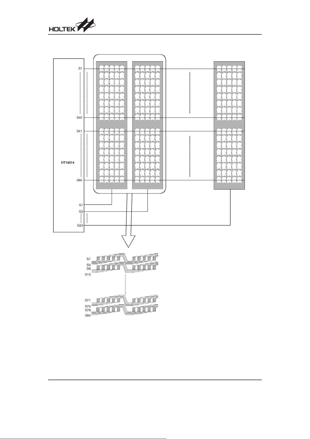
HT16514 Connect to VFD as Below Figure
HT16514
Rev. 1.00 11 October 4, 2006
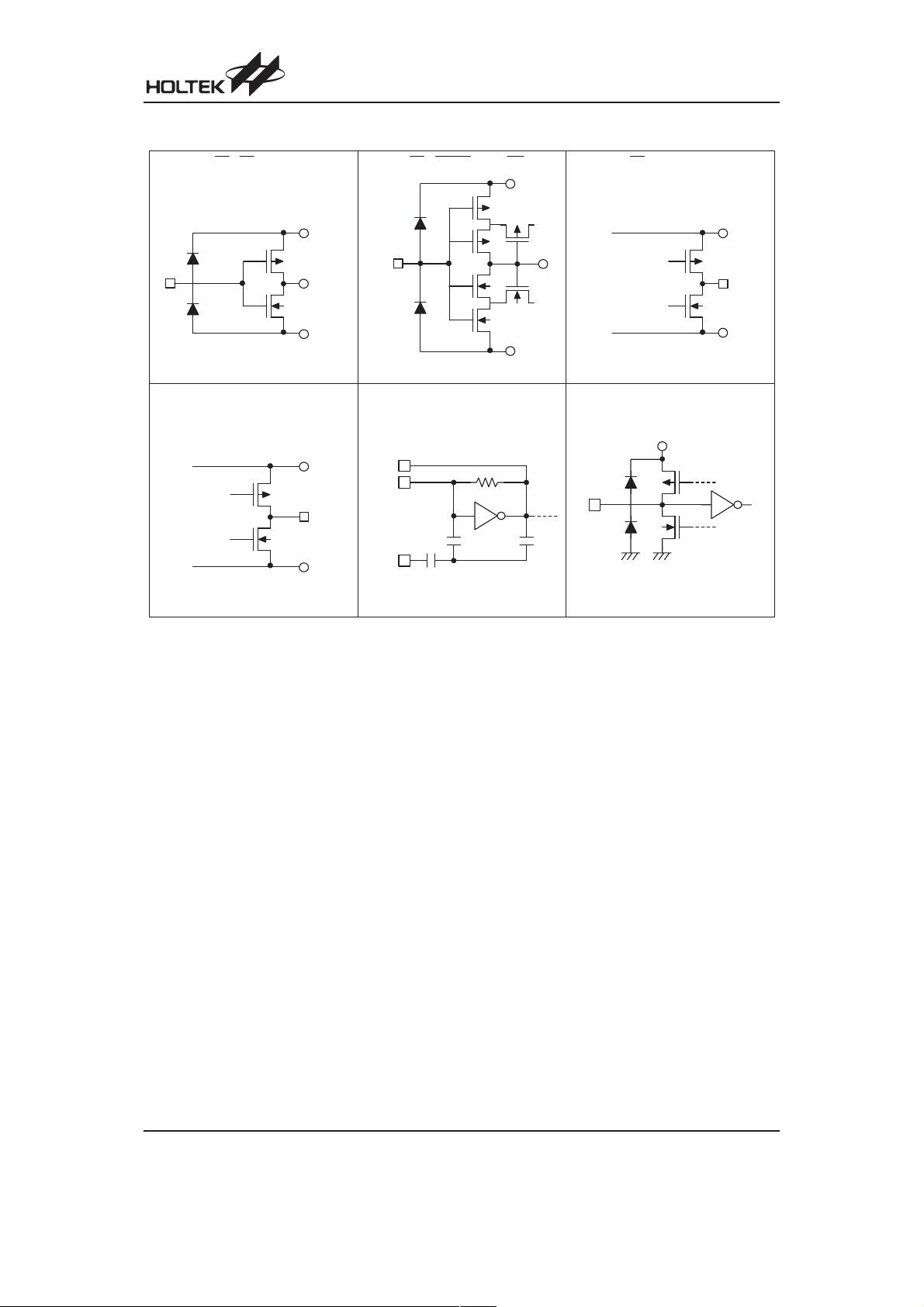
Approximate Internal Connections
HT16514
( M P U ) ( R S , S T ) ( C S ) ( D L S ) ( D S 0 ) ( D S 1 )
( I M ) ( R L 1 ) ( R L 2 ) ( T E S T I )
V
D D
L G N D
S 1 ~ S 8 0 , G 1 ~ G 2 4
V H
P G N D
S L K , E ( R D ) , R E S E T , ( R , W / W R ) S D O , S L K C L , L E , T E S T O
V
D D
L G N D
O S C O , O S C I , X O U T
X O U T
O S C O
O S C I
D 0 ~ D 7 , S I , S O
V
V
D D
L G N D
D D
Absolute Maximum Ratings
Logic Supply Voltage .................VSS-0.3V to VSS+6.0V
Input Voltage..............................V
Driver Output Voltage............................V
-0.3V to VDD+0.3V
SS
-0.3V to V
SS
Driver Output Current (Total) ...................500 (Est.) mA
Driver Supply Voltage .................V
Output Voltage...........................V
Driver Output Current .........................................±50mA
H
Storage Temperature ............................-55°Cto125°C
Operating Temperature...........................-40°Cto85°C
Note: These are stress ratings only. Stresses exceeding the range specified under ²Absolute Maximum Ratings² may
cause substantial damage to the device. Functional operation of this device at other conditions beyond those
listed in the specification is not implied and prolonged exposure to extreme conditions may affect device reliabil
ity.
-0.3V to VSS+80V
SS
-0.3V to VDD+0.3V
SS
-
Rev. 1.00 12 October 4, 2006
 Loading...