

Page 1

H a n n S t a r D i s p l a y C o r p .
p
Document Title HG171A_XY _HSM Page No.
Document No.
Service Manual
Revision
1 / 65
08/09/09
Model Name:HG171A
Model No:HSG1033
17” Color TFT LCD Display
The information contained in this document is the exclusive property of HannStar Display Corporation. It shall not be
disclosed,distributed or re
roduced in whole or in part without written permission of HannStar Display Corporation.
Page 2
H a n n S t a r D i s p l a y C o r p .
p
Document Title HG171A_XY _HSM Page No.
Document No.
Revision
2 / 65
08/09/09
Copyright
Copyright © 2006 by HannStar Corporation. All rights reserved. No part of this publication
may be reproduced, transmitted, transcribed, stored in a retrieval system, or translated into
any
language or computer language, in any form or by any means, electronic, mechanical,
magnetic, optical, chemical, manual or otherwise, without the prior written permission of
HannStar Corporation.
Disclaimer
HannStar makes no representations or warranties, either expressed or implied, with respect to
the contents hereof and specifically disclaims any warranty of merchantability or fitness for
any particular purpose. Further, HannStar reserves the right to revise this publication and to
make changes from time to time in the contents hereof without obligation of HannStar to notify
any person of such revision or changes.
Trademarks
Opt quest is a registered trademark of HannStar Corporation.
HannStar is a registered trademark of HannStar Corporation.
All other trademarks used within this document are the property of their respective owners.
Revision History
Revision SM Editing Date ECR Number Description of Changes TPV Model
A00 Sep.-10-08 First Version Release T7RHM5D8AWHZNC
A01 Dec.-02-08 Add new BOM in item 16 T7RHM5DBAWZ3NN
The information contained in this document is the exclusive property of HannStar Display Corporation. It shall not be
disclosed,distributed or re
roduced in whole or in part without written permission of HannStar Display Corporation.
Page 3

H a n n S t a r D i s p l a y C o r p .
p
Document Title HG171A_XY _HSM Page No.
Document No.
Revision
3 / 65
08/09/09
TABLE OF CONTENTS
1. Dimensions 4
2. Precautions and Safety Notice 6
3.Monitor Specification 7
4.LCD Monitor Description 8
5.Operation Instruction 9
6. Input/output Specification 14
7. Mechanical Instructions 18
8. Block Diagram 21
9.Schematic 27
10.PCB Layout 35
11. Maintainability 41
12 DDC Instruction 47
13. White-Balance, Luminance adjustment 53
14.Monitor Exploded View 55
15. BOM List 56
16.Different Parts List…………………….……………………………………………………….………...65
The information contained in this document is the exclusive property of HannStar Display Corporation. It shall not be
disclosed,distributed or re
roduced in whole or in part without written permission of HannStar Display Corporation.
Page 4
H a n n S t a r D i s p l a y C o r p .
p
Document Title HG171A_XY _HSM Page No.
Document No.
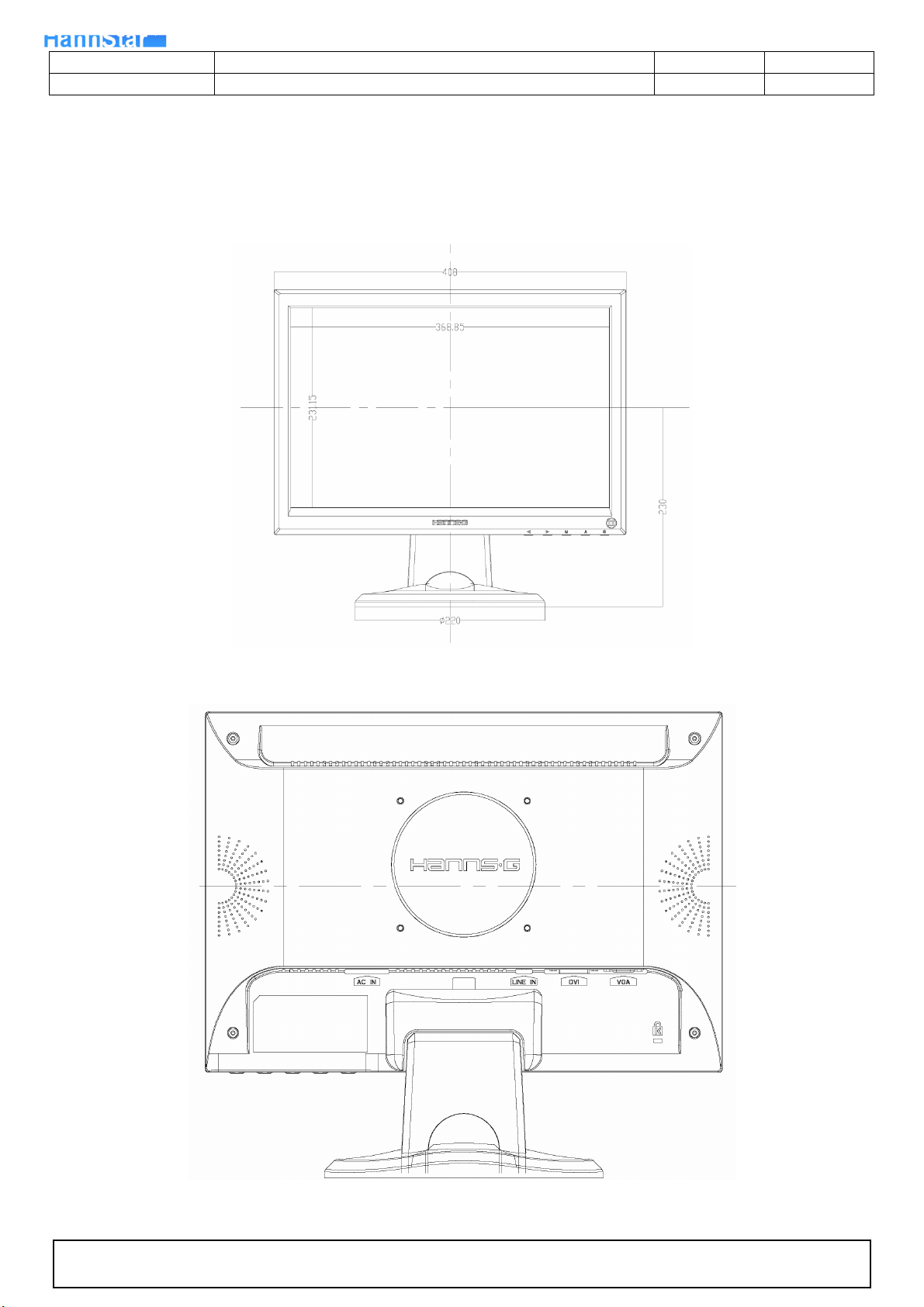
1. Dimensions
1.1 Front View
Revision
4 / 65
08/09/09
1.2 Back View
The information contained in this document is the exclusive property of HannStar Display Corporation. It shall not be
disclosed,distributed or re
roduced in whole or in part without written permission of HannStar Display Corporation.
Page 5
H a n n S t a r D i s p l a y C o r p .
p
Document Title HG171A_XY _HSM Page No.
Document No.
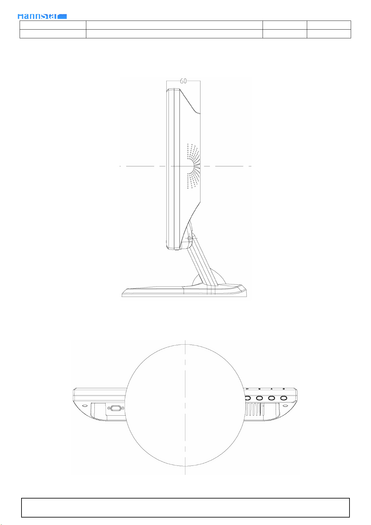
1.3 Side View
Revision
5 / 65
08/09/09
1.4 Bottom View
The information contained in this document is the exclusive property of HannStar Display Corporation. It shall not be
disclosed,distributed or re
roduced in whole or in part without written permission of HannStar Display Corporation.
Page 6

H a n n S t a r D i s p l a y C o r p .
p
Document Title HG171A_XY _HSM Page No.
Document No.
Revision
6 / 65
08/09/09
2. Precautions and Safety Notices
Proper service and repair is important to the safe, reliable operation of all AOC Company Equipment. The service
procedures recommended by AOC and described in this service manual are effective methods of performing service
operations. Some of these service operations require the use of tools specially designed for the purpose. The special tools
should be used when and as recommended.
It is important to note that this manual contains various CAUTIONS and NOTICES which should be carefully read in order
to minimize the risk of personal injury to service personnel. The possibility exists that improper service methods may
damage the equipment. It is also important to understand that these CAUTIONS and NOTICES ARE NOT EXHAUSTIVE.
AOC could not possibly know, evaluate and advise the service trade of all conceivable ways in which service might be
done or of the possible hazardous consequences of each way. Consequently, AOC has not undertaken any such broad
evaluation. Accordingly, a servicer who uses a service procedure or tool which is not recommended by AOC must first
satisfy himself thoroughly that neither his safety nor the safe operation of the equipment will be jeopardized by the service
method selected.
Hereafter throughout this manual, AOC Company will be referred to as AOC.
WARNING
Use of substitute replacement parts, which do not have the same, specified safety characteristics may create shock, fire, or
other hazards.
Under no circumstances should the original design be modified or altered without written permission from AOC. AOC
assumes no liability, express or implied, arising out of any unauthorized modification of design.
Servicer assumes all liability.
FOR PRODUCTS CONTAINING LASER:
DANGER-Invisible laser radiation when open AVOID DIRECT EXPOSURE TO BEAM.
CAUTION-Use of controls or adjustments or performance of procedures other than those specified herein may result in
hazardous radiation exposure.
CAUTION -The use of optical instruments with this product will increase eye hazard.
TO ENSURE THE CONTINUED RELIABILITY OF THIS PRODUCT, USE ONLY ORIGINAL MANUFACTURER'S
REPLACEMENT PARTS, WHICH ARE LISTED WITH THEIR PART NUMBERS IN THE PARTS LIST SECTION OF THIS
SERVICE MANUAL.
Take care during handling the LCD module with backlight unit.
-Must mount the module using mounting holes arranged in four corners.
-Do not press on the panel, edge of the frame strongly or electric shock as this will result in damage to the screen.
-Do not scratch or press on the panel with any sharp objects, such as pencil or pen as this may result in damage to the
panel.
-Protect the module from the ESD as it may damage the electronic circuit (C-MOS).
-Make certain that treatment person’s body is grounded through wristband.
-Do not leave the module in high temperature and in areas of high humidity for a long time.
-Avoid contact with water as it may a short circuit within the module.
‐Ifthesurfaceofpanelbecomesdirty,pleasewipeitoffwithasoftmaterial.(Cleaningwithadirtyorroughclothmaydamage
thepanel.)
The information contained in this document is the exclusive property of HannStar Display Corporation. It shall not be
disclosed,distributed or re
roduced in whole or in part without written permission of HannStar Display Corporation.
Page 7
H a n n S t a r D i s p l a y C o r p .
p
Document Title HG171A_XY _HSM Page No.
Document No.
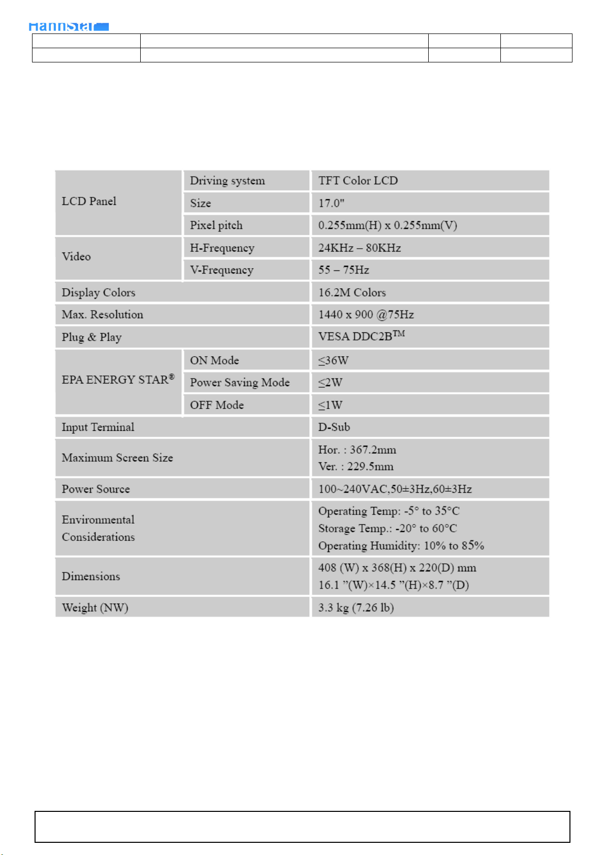
3. Monitor Specifications
Revision
7 / 65
08/09/09
The information contained in this document is the exclusive property of HannStar Display Corporation. It shall not be
disclosed,distributed or re
roduced in whole or in part without written permission of HannStar Display Corporation.
Page 8
H a n n S t a r D i s p l a y C o r p .
p
Document Title HG171A_XY _HSM Page No.
Document No.
Revision
8 / 65
08/09/09
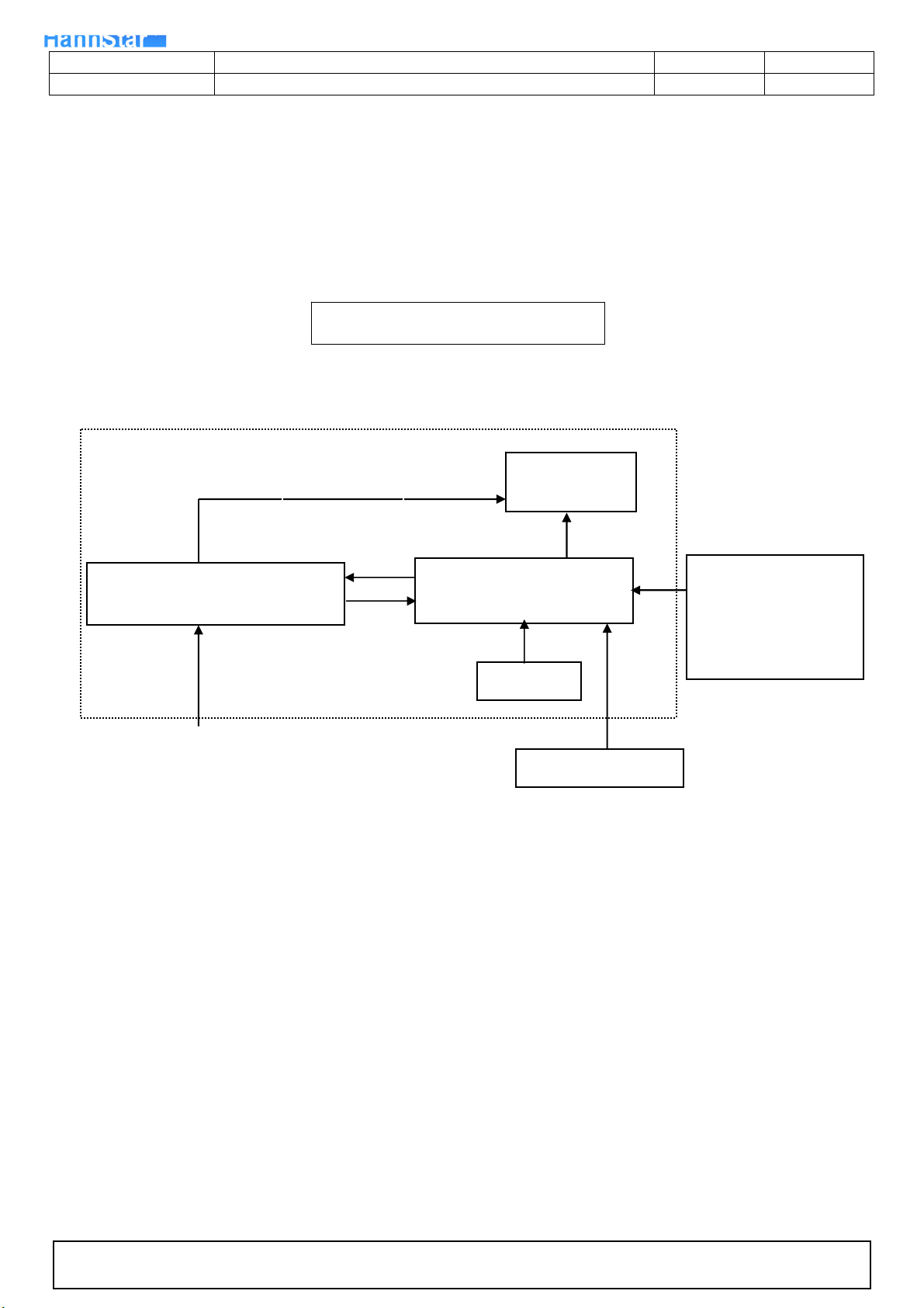
4. LCD Monitor Description
Assembly Description
The LCD MONITOR will contain a main board, a power board, and a key board which house the flat panel control logic,
brightness control logic and DDC.
The power board will provide AC to DC Inverter voltage to drive the backlight of panel and the main board chips each
voltage.
CCFL Drive.
Power board
(Include: adapter, inverter)
Monitor Block Diagram
Flat Panel and
CCFL backlight
main board
RS232 Connector
For white balance
adjustment in factory
mode
AC-IN
100V-240V
Key board
HOST Computer
Video signal, DDC
The information contained in this document is the exclusive property of HannStar Display Corporation. It shall not be
disclosed,distributed or re
roduced in whole or in part without written permission of HannStar Display Corporation.
Page 9
H a n n S t a r D i s p l a y C o r p .
p
Document Title HG171A_XY _HSM Page No.
Document No.
Revision
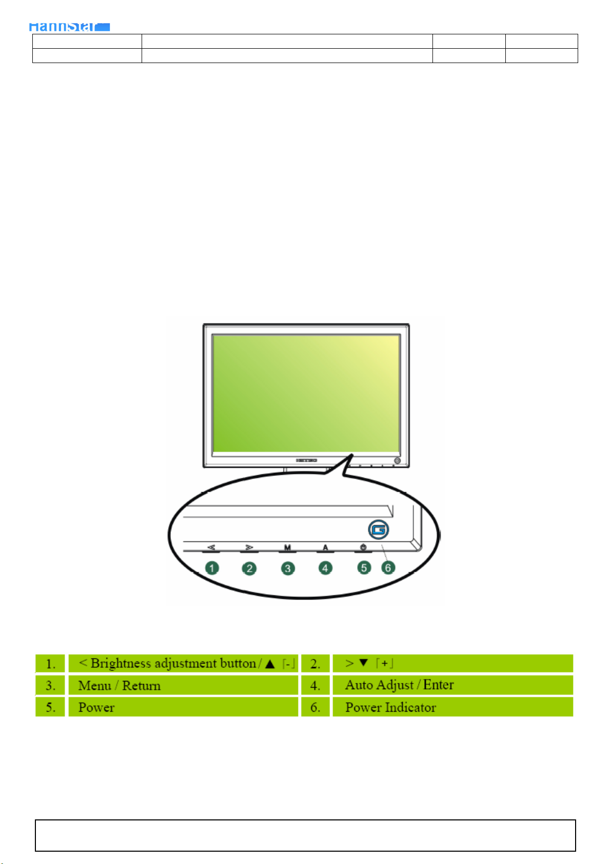
5. Operating Instructions
5.1 General Instructions
Press the power button to turn the monitor on or off. The control buttons are located in the front of the monitor.
By changing these settings, the picture can be adjusted to your personal preferences.
The power cord should be connected.
-
Connect the video cable from the monitor to the video card.
-
Press the power button to turn on the monitor, the power indicator will light up.
-
5.2 Control Buttons
9 / 65
08/09/09
The information contained in this document is the exclusive property of HannStar Display Corporation. It shall not be
disclosed,distributed or re
roduced in whole or in part without written permission of HannStar Display Corporation.
Page 10

H a n n S t a r D i s p l a y C o r p .
p
Document Title HG171A_XY _HSM Page No.
Document No.
FRONT PANEL CONTROL
• Power Button:
Press this button to switch ON/OFF of monitor’s power.
• Power Indicator:
Green — Power On mode.
Orange — Power Saving mode.
• MENU / ENTER:
1. Turn the OSD menu on/off or return to the previous menu
2. Exit OSD menu when in volume OSD status.
Revision
10 / 65
08/09/09
• Adjust < >:
1. Activates the volume control when the OSD is OFF.
2. Navigate through adjustment icons when OSD is ON or adjust a function when function is activated.
• A Button:
• The OSD menu is used as ¡§confirmation¡¨ function during start-up. 2. Press and hold this button more than 3 seconds
will start 「Auto Adjust」 function when using VGA input only. (The auto adjustment function is used to optimize the
「horizontal position」, 「vertical position」,「clock」,and 「phase」.)
NOTES:
• Do not install the monitor in a location near heat sources such as radiators or air dusts, or in a place subject to direct
sunlight, or excessive dust or mechanical vibration or shock.
• Save the original shipping box and packing materials, as they will come in handy if you ever have to ship your monitor.
• For maximum protection, repackage your monitor as it was originally packed at the factory.
• To keep the monitor looking new, periodically clean it with a soft cloth. Stubborn stains may be removed with a cloth
lightly dampened with a mild detergent solution. Never use strong solvents such as thinner, benzene, or abrasive
cleaners, since these will damage the cabinet. As a safety precaution, always unplug the monitor before cleaning it.
• Function Key Lock:
Press the 「<」, 「>」 and the 「Menu」 buttons simultaneously to enable the Function Key Lock. When the Function Key
Lock is enabled, only the Power button is active. Press the 「<, 「>」 and the 「Menu」buttons simultaneously again to
unlock the function keys.
The information contained in this document is the exclusive property of HannStar Display Corporation. It shall not be
disclosed,distributed or re
roduced in whole or in part without written permission of HannStar Display Corporation.
Page 11
H a n n S t a r D i s p l a y C o r p .
p
Document Title HG171A_XY _HSM Page No.
Document No.
5.3 Adjusting the Picture
Revision
11 / 65
08/09/09
The information contained in this document is the exclusive property of HannStar Display Corporation. It shall not be
disclosed,distributed or re
roduced in whole or in part without written permission of HannStar Display Corporation.
Page 12
H a n n S t a r D i s p l a y C o r p .
p
Document Title HG171A_XY _HSM Page No.
Document No.
Revision
12 / 65
08/09/09
The information contained in this document is the exclusive property of HannStar Display Corporation. It shall not be
disclosed,distributed or re
roduced in whole or in part without written permission of HannStar Display Corporation.
Page 13
H a n n S t a r D i s p l a y C o r p .
p
Document Title HG171A_XY _HSM Page No.
Document No.
Revision
13 / 65
08/09/09
The information contained in this document is the exclusive property of HannStar Display Corporation. It shall not be
disclosed,distributed or re
roduced in whole or in part without written permission of HannStar Display Corporation.
Page 14
H a n n S t a r D i s p l a y C o r p .
p
Document Title HG171A_XY _HSM Page No.
Document No.
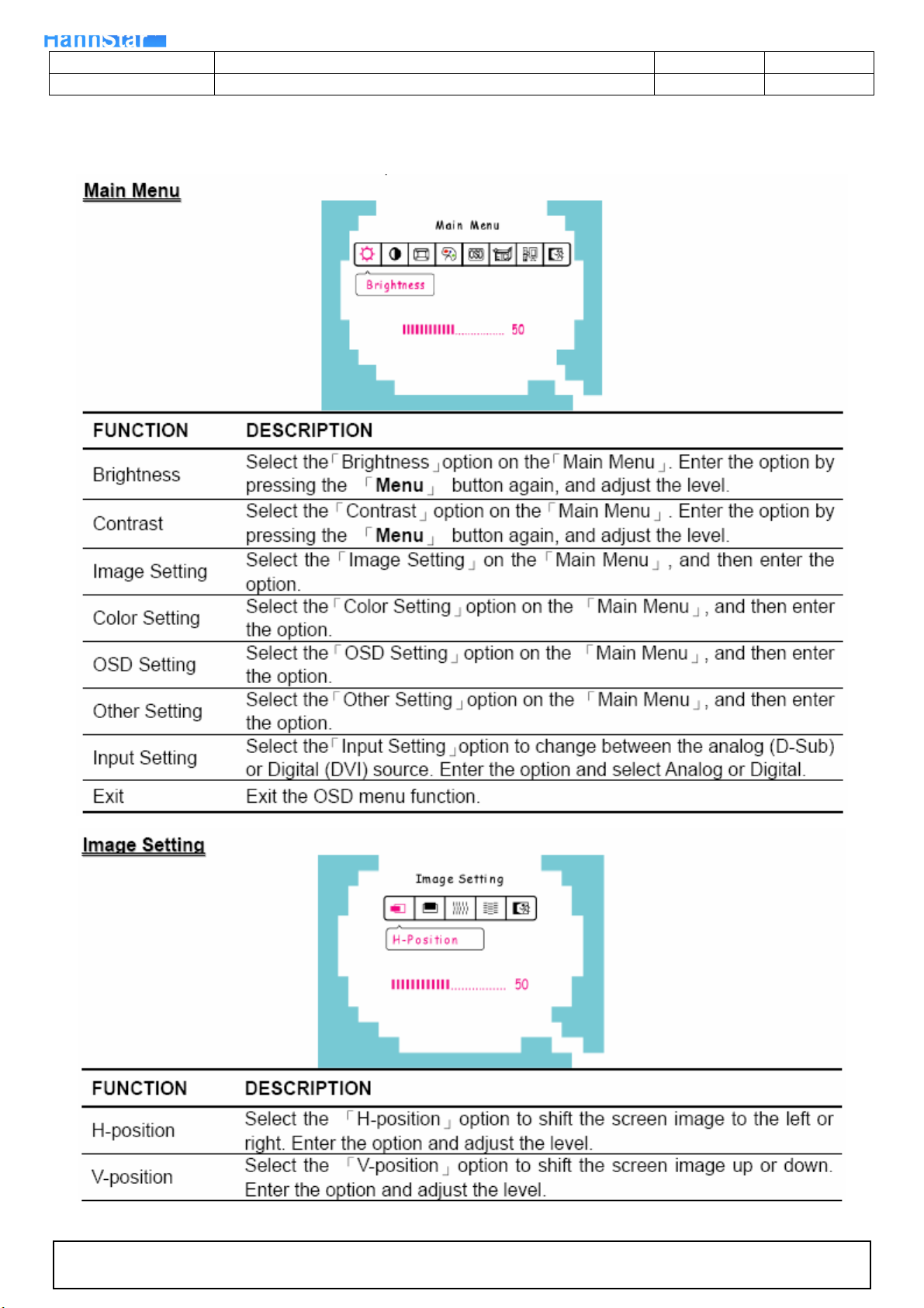
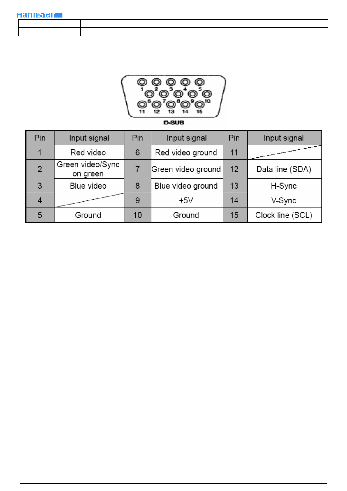
6. Input/output Specification
6.1 Input Signal Connector
Revision
14 / 65
08/09/09
The information contained in this document is the exclusive property of HannStar Display Corporation. It shall not be
disclosed,distributed or re
roduced in whole or in part without written permission of HannStar Display Corporation.
Page 15
H a n n S t a r D i s p l a y C o r p .
p
Document Title HG171A_XY _HSM Page No.
Document No.
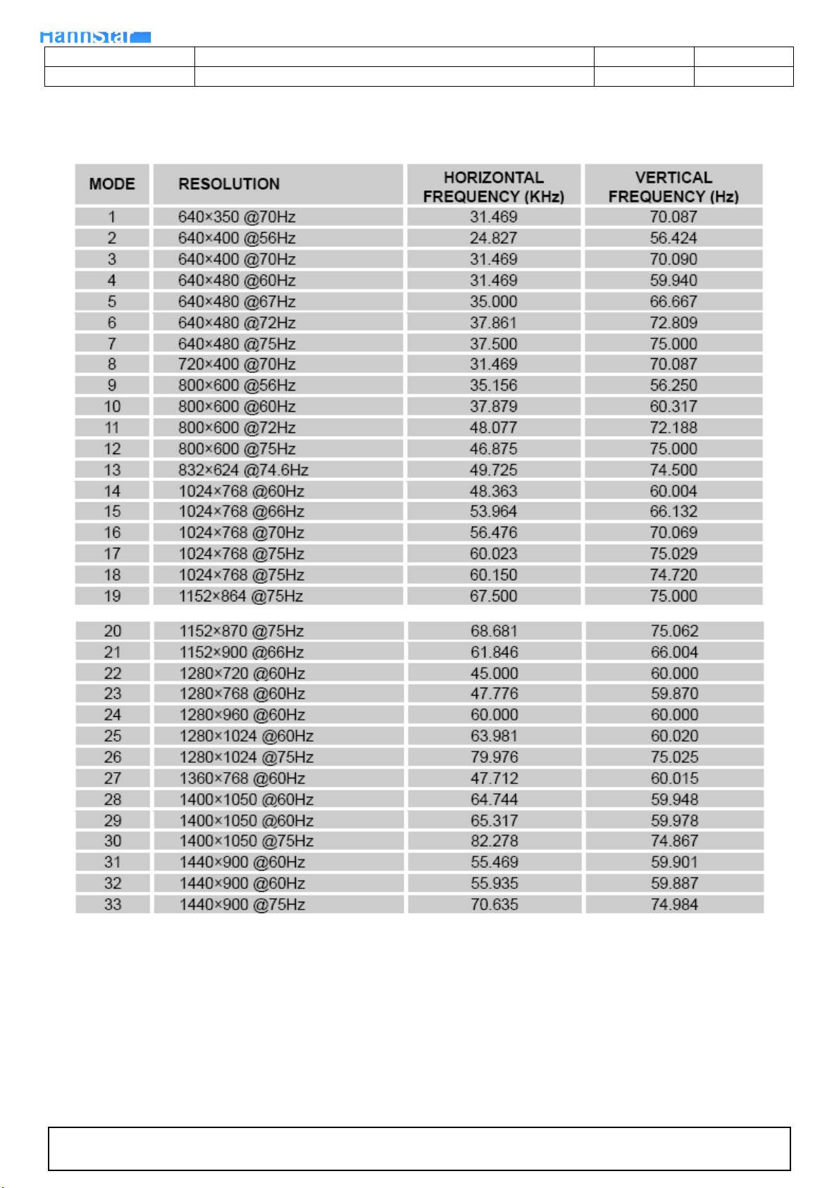
6.2 Factory Preset Display Modes
Revision
15 / 65
08/09/09
The information contained in this document is the exclusive property of HannStar Display Corporation. It shall not be
disclosed,distributed or re
roduced in whole or in part without written permission of HannStar Display Corporation.
Page 16
H a n n S t a r D i s p l a y C o r p .
p
Document Title HG171A_XY _HSM Page No.
Document No.
Revision
16 / 65
08/09/09
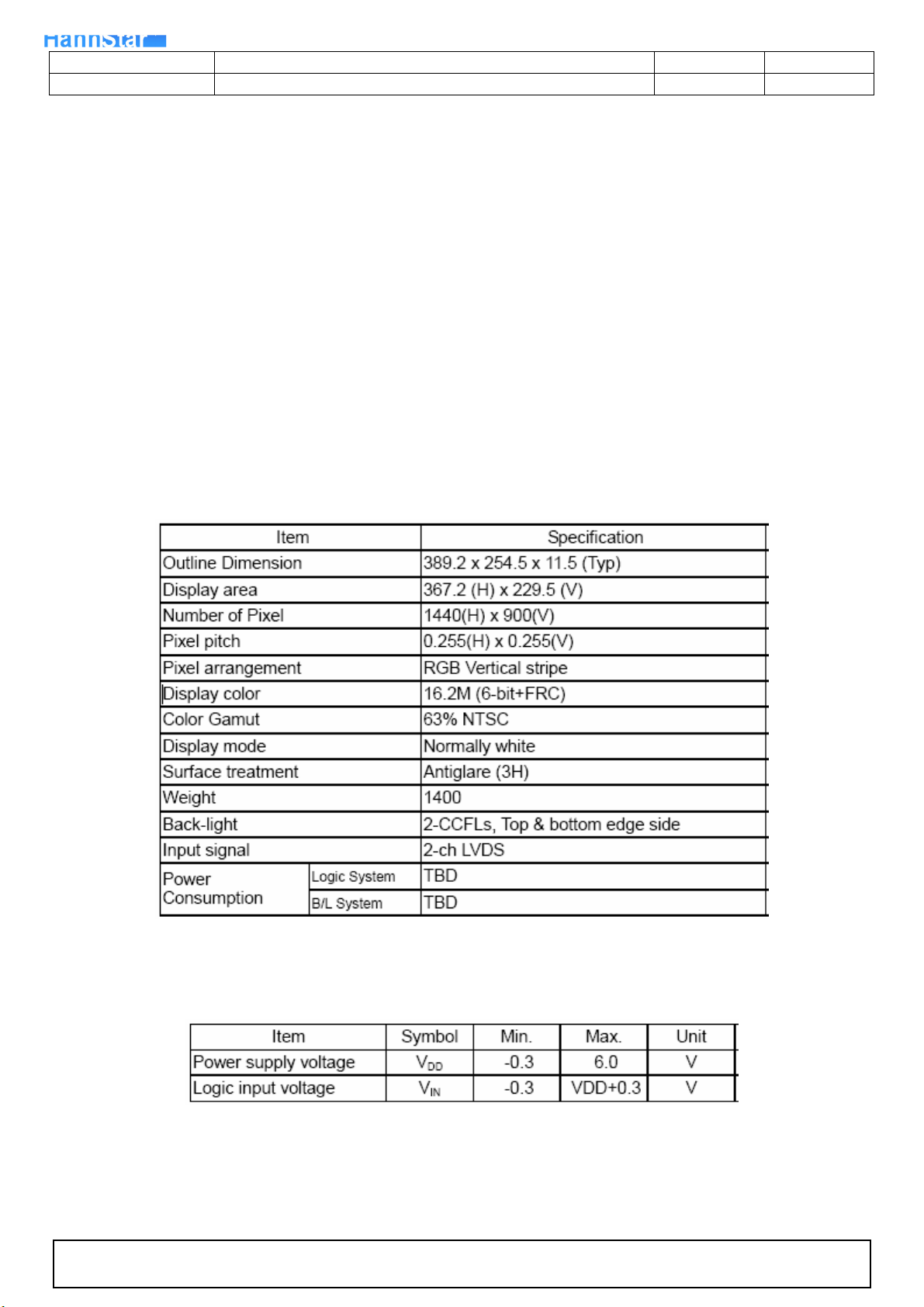
6.3 Panel Specification
HannStar Display model HSD170MGW1-B00 is a color active matrix thin film transistor(TFT) liquid crystal display (LCD)
that uses amorphous silicon TFT as a switching device. This model is composed of a TFT LCD panel, a driving circuit and
a back light system. This TFT LCD has a 17.0 inch diagonally measured active display area with
XGA resolution (900 vertical by 1440 horizontal pixel array) and can display up to 16.2M (6-bit+FRC)colors.
6.3.1 Features
_ 17.0 WXGA+ for Monitor application
_ High Resolution: 1440*900
_ 2-ch LVDS interface system
_ LCD Timing Controller
_ Wide Viewing Angle
_ RoHS compliance
6.3.2 Display Characteristics
6.3.3 Electrical Characteristics
1. TFT LCD Module
The information contained in this document is the exclusive property of HannStar Display Corporation. It shall not be
disclosed,distributed or re
roduced in whole or in part without written permission of HannStar Display Corporation.
Page 17

H a n n S t a r D i s p l a y C o r p .
p
Document Title HG171A_XY _HSM Page No.
Document No.
2. Backlight Unit
6.3.4 Optical Characteristics
Measuring Condition
_ Measuring surrounding: dark room
_ Lamp current IBL: 7.5±0.1mA, lamp freq. FL=50 KHz, Inverter: TDK TBD315NR-1
_ VDD=5.0V, fV=60Hz
_ Ambient temperature: 25±2oC
_ 30min. Warm-up time.
Revision
17 / 65
08/09/09
The information contained in this document is the exclusive property of HannStar Display Corporation. It shall not be
disclosed,distributed or re
roduced in whole or in part without written permission of HannStar Display Corporation.
Page 18
H a n n S t a r D i s p l a y C o r p .
p
Document Title HG171A_XY _HSM Page No.
Document No.
Revision
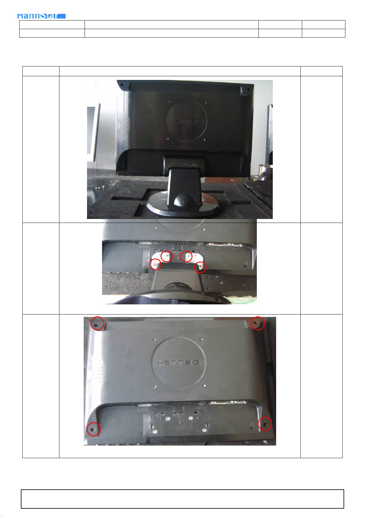
7. Mechanical Instructions
Step Figure Description
18 / 65
08/09/09
Preparati
on
Remove
the base
Lay the LCD
on a flat, soft
and clean
surface.
Remove the
screws
remarked in
red
Remove the
Remove
rear cover
screws
remarked in
red
The information contained in this document is the exclusive property of HannStar Display Corporation. It shall not be
disclosed,distributed or re
roduced in whole or in part without written permission of HannStar Display Corporation.
Page 19
H a n n S t a r D i s p l a y C o r p .
p
Document Title HG171A_XY _HSM Page No.
Document No.
Revision
19 / 65
08/09/09
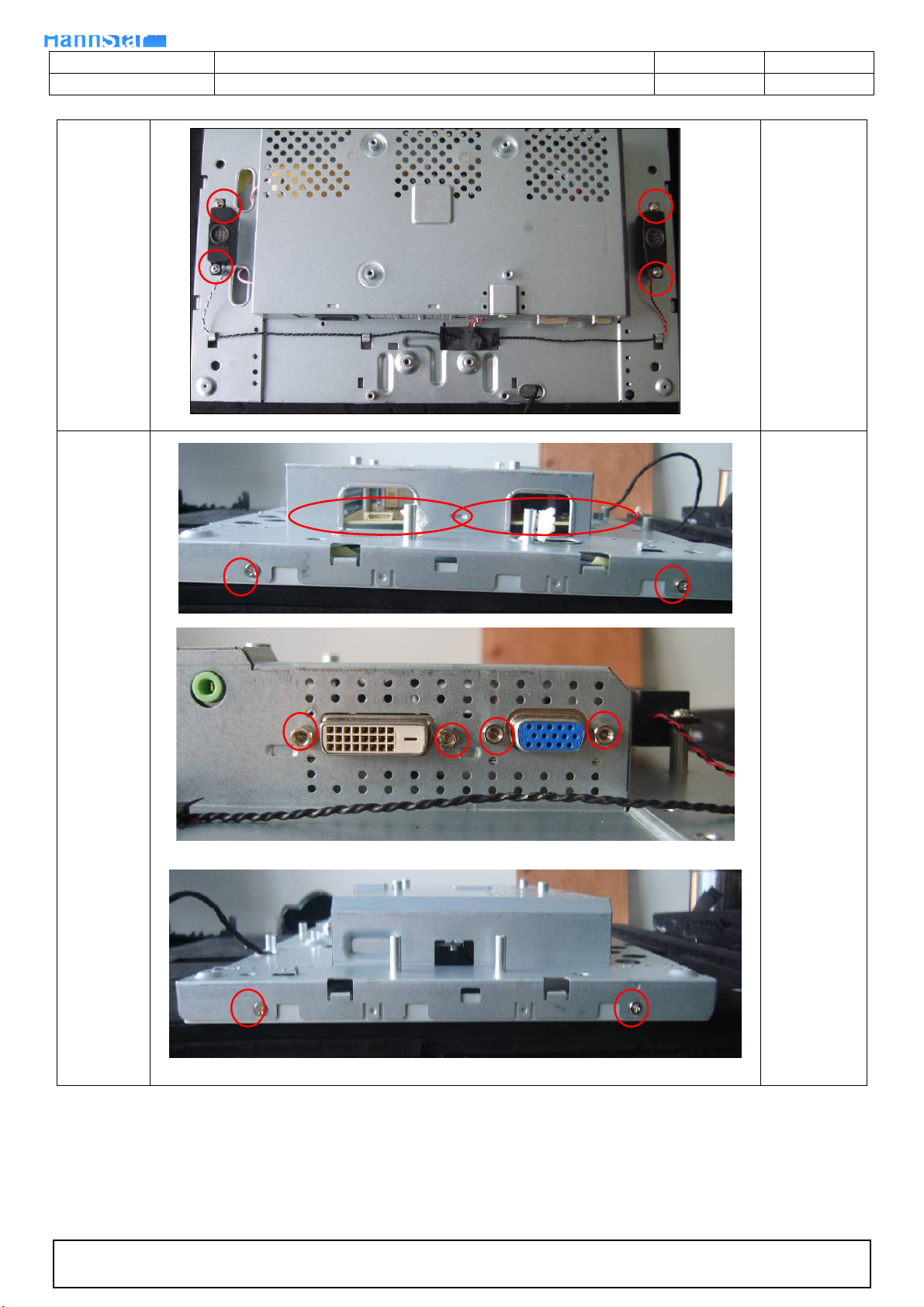
Remove
the
speaker
remove
the shield
Remove the
screws
remarked in
red
Remove the
screws
remarked in
red and
disconnecte
d the
connecter
remarked in
red
(HG171A:
NO DVI )
The information contained in this document is the exclusive property of HannStar Display Corporation. It shall not be
disclosed,distributed or re
roduced in whole or in part without written permission of HannStar Display Corporation.
Page 20
H a n n S t a r D i s p l a y C o r p .
p
Document Title HG171A_XY _HSM Page No.
Document No.
Revision
20 / 65
08/09/09
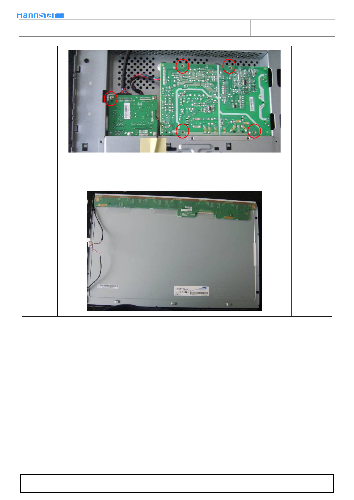
Remove
the
boards
The end
Remove the
screws
remarked in
red
The panel
The information contained in this document is the exclusive property of HannStar Display Corporation. It shall not be
disclosed,distributed or re
roduced in whole or in part without written permission of HannStar Display Corporation.
Page 21

H a n n S t a r D i s p l a y C o r p .
p
Document Title HG171A_XY _HSM Page No.
Document No.
8. Block Diagram
8.1 Software Flow Chat
1
Revision
21 / 65
08/09/09
2
N
4
5
Y
6
7
Y
Y
N
N
3
18
9
10
Y
N
N
12
Y
14
19
N
11
13
15
17
N
Y
N
Y
16
Y
The information contained in this document is the exclusive property of HannStar Display Corporation. It shall not be
disclosed,distributed or re
roduced in whole or in part without written permission of HannStar Display Corporation.
Page 22

H a n n S t a r D i s p l a y C o r p .
p
Document Title HG171A_XY _HSM Page No.
Document No.
Revision
22 / 65
1) MCU initialize.
2) Is the EPROM blank?
3) Program the EPROM by default values.
4) Get the PWM value of brightness from EPROM.
5) Is the power key pressed?
6) Clear all global flags.
7) Are the AUTO and SELECT keys pressed?
8) Enter factory mode.
9) Save the power key status into EPROM.
Turn on the LED and set it to green color.
Scalar initializes.
10) In standby mode?
11) Update the lifetime of back light.
12) Check the analog port, are there any signals coming?
13) Does the scalar send out an interrupt request?
14) Wake up the scalar.
15) Are there any signals coming from analog port?
16) Display "No connection Check Signal Cable" message. And go into standby mode after the message
disappear.
17) Program the scalar to be able to show the coming mode.
18) Process the OSD display.
19) Read the keyboard. Is the power key pressed?
08/09/09
The information contained in this document is the exclusive property of HannStar Display Corporation. It shall not be
disclosed,distributed or re
roduced in whole or in part without written permission of HannStar Display Corporation.
Page 23

H a n n S t a r D i s p l a y C o r p .
p
Document Title HG171A_XY _HSM Page No.
Document No.
8.2 Electrical Block Diagram
8.2.1 Main Board
Analog
Input
YPbPr
Input
RGB/HS/VS
SCALER IC
IC
TSUM1PFR-LF
Revision
LVD S
Output
23 / 65
08/09/09
DC
Power In
Keypad
12V
5V/3V3/1V8
Keypad
AMP
TDA7496L
MCU
RTD2120L
The information contained in this document is the exclusive property of HannStar Display Corporation. It shall not be
disclosed,distributed or re
roduced in whole or in part without written permission of HannStar Display Corporation.
Page 24

H a n n S t a r D i s p l a y C o r p .
p
Document Title HG171A_XY _HSM Page No.
Document No.
8.2.2 Power/Inverter Board
AC input
Lamp
EMI filter
Start Circuit: R904,R932,R933
Output
Circuit
Feedback
Circuit
Bridge
Rectifier
and Filter
PWM
Control IC
Over
Voltage
Transformer
Transformer
Rectifier
diodes
Feedback
Circuit
MOSFET
PWM
Control IC
ON/OFF
Control
DIM
DIM
Revision
12V
ON/OFF
24 / 65
08/09/09
CN902
5V
The information contained in this document is the exclusive property of HannStar Display Corporation. It shall not be
disclosed,distributed or re
roduced in whole or in part without written permission of HannStar Display Corporation.
Page 25

H a n n S t a r D i s p l a y C o r p .
p
A
Document Title HG171A_XY _HSM Page No.
Document No.
8.3 Mechanical Block Diagram
8.3.1 Assembly Block
Main Board*1
Screw*1
Bezel*1
Len *1
Assy,base*1
Screw*4
Rubber Foot*4
Speaker*2
Screw*4
Main Frame
HG171
Assy,Bezel*1
Button*1
Back Cover*1
Assay Stand*1
LCD Monitor
,Panel *1
Screw*4
HG171A
Power Board
Screw*4
Key Board *1
Keypad cable*1
Stand*1
Hinge*1
Assy stand*1
Revision
25 / 65
08/09/09
The information contained in this document is the exclusive property of HannStar Display Corporation. It shall not be
disclosed,distributed or re
roduced in whole or in part without written permission of HannStar Display Corporation.
Page 26

H a n n S t a r D i s p l a y C o r p .
p
A
,
Document Title HG171A_XY _HSM Page No.
Document No.
8.3.1 Disassembly Block
HG171A
LCD Monitor
Assy Base*1
Rubber foot
Base*1
Revision
26 / 65
08/09/09
Bezel*1
Len *1
Main Board*1
Screw*1
Assy Stand*1
Back Cover*1
Assy,Bezel*1
Button*1
Main Frame
HG171
Panel *1
Speaker*2
Screw*4
Stand*1
Hinge*1
Key Board *1
Keypad cable*1
Screw*2
Power Board
Screw*4
The information contained in this document is the exclusive property of HannStar Display Corporation. It shall not be
disclosed,distributed or re
roduced in whole or in part without written permission of HannStar Display Corporation.
Page 27

H a n n S t a r D i s p l a y C o r p .
p
Document Title HG171A_XY _HSM Page No.
Document No.
9. Schematic
9.1 Main Board
Revision
TSUM16FWR SCHEMATIC
27 27/65
08/09/09
ESD_VCC
CMVCC1
VCC 3.3
CMVCC
ESD_VCC
DSUB_5V
DSUB_5V
VCC 3.3
XGA/SXGA
DSUB_5V
ESD_VCC
VCC 3.3
02.Input
VCC 1.8
VCC1. 8
VCC 3.3
CMVCC
CMVCC1
DET_CABLE
on_BACKLI GHT
Adj_BACKLI GHT
DSUB_R+
DSUB_R-
DSUB_G+
DSUB_G-
DSUB_SOG
DSUB_B+
DSUB_B-
DSUB_H
DSUB_V
DDC1_SDA
DDC1_SCL
Mut e
Volume#
PANEL_I D#DSUB_5V
VCTRL
DSUB_R+
DSUB_RDSUB_G+
DSUB_G-
DSUB_SOG
DSUB_B+
DSUB_BDSUB_H
DSUB_V
DDC1_SDA
DDC1_SCL
DET_CABLE
on_BACKLI GHT
Mut e
Volume#
PANEL_I D#
Adj_BACKLI GHT
VCTRL
LVDS OUTPUT
VCC 1.8
VCC1.8
VCC 3.3
CMVCC
CMVCC1
PA[0. .1]
PA[4. .9]
PB[0. .9]
PPWR _ON#
VCC 3.3
PA[0. .1]
PA[4. .9]
PB[0. .9]
CMVCC
CMVCC1
PA[0..1]
PA[4..9]
PB[0..9]
PPWR _ON#
CMVCC
CMVCC
ESD_VCC
05.Pow e r
03.Scala r
04.Output
The information contained in this document is the exclusive property of HannStar Display Corporation. It shall not be disclosed,distributed or reproduced in whole or
in
art without written permission of HannStar Display Corporation.
Page 28

H a n n S t a r D i s p l a y C o r p .
p
Document Title HG171A_XY _HSM Page No.
Document No.
DDC1_SCL5
DDC1_SDA5
R120
10K 1/16W 5%
DDC1_SCL
DDC1_SDA
GND POWER
DSUB_SDA
DSUB_SCL
VGA_G+
VGA_R+
VCC3.3
R121
10K 1/16W 5%
R110
100R 1/16W 5%
R113
100R 1/16W 5%
DGND
U103
1
I/O1
I/O4
2
GND
VDD
3 4
I/O2 I/O3
AZC099-04S
U102
1
I/O1
I/O4
2
GND
VDD
3 4
I/O2 I/O3
AZC099-04S
DSUB_SCL
DSUB_SDA
6
5
6
5
H_Sync
V_Sync
VGA_B+
H_Sync
V_Sy nc
15
14
13
12
11
ESD_VCC
候綼
U103
ESD_VCC
R101 0R05 1/10W 5%
2K2 1/16W 5%
CN101
DB15
17 16
ESD_VCC 5
C115
NC
C114
NC
R105
10
5
9
4
8
3
7
2
6
1
R106
2K2 1/16W 5%
DSUB_5V
VGA_BVGA_B+
VGA_G-
ZD103
UDZSNP5.6B
VGA_G+ FB103
VGA_RVGA_R+
C102
22pF
VGA_PLUG
1 2
R102 100R 1/16W 5%
R103 100R 1/16W 5%
C103
22pF
DSUB_5V
ZD104
UDZ SNP5.6B
1 2
DSUB_5V 5
DSUB_H 5
DSUB_V 5
VGA_B+
VGA_B-
VGA_G+
VGA_G-
VGA_R+
VGA_R-
FB102
1 2
BEAD
1 2
BEAD
FB101
1 2
BEAD
R107
75R 1/16W 5%
R112
75R 1/16W 5%
R116
75R 1/16W 5%
100R 1/16W 5%
C104
5pF/50V
100R 1/16W 5%
390 OHM 1/16W
100R 1/16W 5%
C108
5pF/50V
100R 1/16W 5%
100R 1/16W 5%
C111
5pF/50V
100R 1/16W 5%
Revision
R104
R108
R109
R111
R114
R115
R117
VGA_PLUG
C101
0.047uF
C105
0.047uF
C106
0.047uF
C107
0.047uF
C109
0.047uF
C110
0.047uF
C113
0.047uF
VCC3.3
R118
1K 1/16W 5%
28 28/65
08/09/09
DSUB_B+ 5
DSUB_B- 5
DSUB_SOG 5
DSUB_G+ 5
DSUB_G- 5
DSUB_R+ 5
DSUB_R- 5
VCC3.3 7
DET_CABLE 5
T P V ( Top Victory Electronics Co . , Ltd. )
Date
G2904-1D-2-X-4-080728
02.Input
絬 隔 瓜 絪 腹
Key Component
OEM MO DE L Size
TPV MOD EL
PCB NA ME
Sheet
HG171A
715G2904-1D
47Monday, July 21, 2008
of
Rev
称爹
B
F
称爹
>
<
The information contained in this document is the exclusive property of HannStar Display Corporation. It shall not be disclosed,distributed or reproduced in whole or
in
art without written permission of HannStar Display Corporation.
Page 29

H a n n S t a r D i s p l a y C o r p .
p
Document Title HG171A_XY _HSM Page No.
Document No.
CMVCC5, 6
CN404
1
2
3
CMVCC
4
CMVCC
5
BKLT-VBRI
6
BKLT-EN
7
C_PANEL_INDEX
8
Volume
9
Mut e
CONN
CMVCC
D403
BAT54C
SM340A
D402
R450 NC
2
NC(R 0402)
3
1
PANEL_I D# 5
2
DSUB_5V
1
3
CMVCC1
D401
BAV99
R449
NC
ESD_VCC 2
DSUB_5V 2
CMVCC1 5
Mut e 5
BKLT-EN
C425
NC
VCC3.3
R437
10K 1/16W 5%
Q406
2N3904S-RTK/PS
VCC3.3
R440
4K7 1/16W 5%
R439
10K 1/16W 5%
on_BACKLI GHT 5
VCTRL5
VCC3.3
Revision
Q410
KN2907AS
Q409
KN2907AS
C432
0.1uF /16V
08/09/09
VCC1.8
+
C423
100UF 25V
29 29/65
VCC1.8 5
VCC3.3
R448
4K7 1/16W 5%
R447
10K 1/16W 5%
Volume# 5
CMVCC1
T P V ( Top Victory Electronics Co . , Ltd. )
絬 隔 瓜 絪 腹
Key Component
G2904-1D-2-X-4-080728
05.Power
Date
C426
+
100UF25V
MVC C
C428
0.1uF/16V
FB403 NC
VCC3.3
3
VIN
2
VOUT
1
ADJ(GND)
U404
AP1117D33LA
OEM MO DE L Size
TPV MO DEL
PCB NAME
Sheet
C422
0.1uF/16V
HG171A
715G2904-1D
77Monday, July 21, 2008
of
+
C427
100UF25V
VCC3.3 4, 5
Rev
称爹
B
F
称爹
>
<
BKLT-VBRI
VCC3.3
R441
1K 1/16W 5%
100R 1/16W 5%
R442
adj_BACKLI GHT 5
Volume
VCC3.3
R446
NC
Q408
2N3904S-RTK/PS
The information contained in this document is the exclusive property of HannStar Display Corporation. It shall not be disclosed,distributed or reproduced in whole or
in
art without written permission of HannStar Display Corporation.
Page 30

H a n n S t a r D i s p l a y C o r p .
p
Document Title HG171A_XY _HSM Page No.
Document No.
Revision
30 30/65
VDDC
U401
R403 390 OHM 1/16W
C401
0.1uF/16V
R401
0R05 1/16W
0R05 1/16W
R402
13
RIN0P
12
RIN0M
10
GIN0P
9
GIN0M
11
SOGIN0
8
BIN0P
7
BIN0M
16
HSYNC0
17
VSYNC0
18
DDCA_SDA/RS232_TX
19
DDCA_SCL/rs232_RX
4
REXT
15
REFP
14
REFM
21
SDO
22
SCZ
23
SCK
24
SDI
28
GPIO_P27/PWM1
54
RST
1
XIN
2
XOU T
31
MODE [0]
32
MODE [1]
DSUB_R+3
DSUB_R-3
DSUB_G+3
DSUB_G-3
DSUB_SOG3
DSUB_B+3
DSUB_B-3
DSUB_H3
DSUB_V3
DDC1_SDA3
DDC1_SCL3
AVDD
VCC3. 3
C408
0.22uF16V
R408
10K 1/16W 5%
CMVCC1
CMVCC17
CMVCC7
10UF50V
CMVCC
C410
C430
NC
+
+
1
CE#
2
SO
3
WP
WP#
4 5
VSS SI
R417
10K 1/16W 5%
R460
NC
U402
8
VDD
7
HOLD#
6
SCK
SST25LF020A-33-4C-SAE
C411 22pF
C412 22pF
R456 0R05 1/16W
R457 0R05 1/16W
R405 100R 1/16W 5%
X401
14.31818MHz
1 2
6
51
VDDP
AVDD_ADC
LVDS
GND
GND
GND
5
29573
TSUM1PFR-LF
30
53
VCTRL
VDDC
VDDC
LVA3P
LVA3M
LVA2P
LVA2M
LVA1P
LVA1M
LVA0P
LVA0M
LVB3P
LVB3M
LVBCKP
LVBCKM
LVB2P
LVB2M
LVB1P
LVB1M
LVB0P
LVB0M
GPIO_P15/PWM0
PWM2/GPIO_P24
GPIO_P12
PWM1/GPIO_P25
RSTN
GPIO_P00/SAR1
GPIO_P01/SAR2
GPIO_P06
GPIO_P07
PWM0/GPIO_P26
GPIO_P13
GPIO_P14
GPIO_P10/I2C_MCL
GPIO_P11/I2C _MDA
52
33
34
35
36
37
38
39
40
41
42
43
44
45
46
47
48
49
50
R424 NC
20
27
55
56
R411 100R 1/16W 5%
58
R412 100R 1/16W 5%
59
R414 120R 1/16W 5%
60
R410 120R 1/16W 5%
61
R418 100R 1/16W 5%
62
63
64
R419 100R 1/16W 5%
26
R413 100R 1/16W 5%
25
VCC3.37
VCC1.87
EE_WP
C418
NC
R426 NC
R452 NC
R420 100R 1/16W 5%
R451 NC
R425
NC
VCTRL 7
PA[0..1] 5
PA[4..9] 5
PB[0..9] 5
on_BACKLIGHT 7
adj_BACKLIGHT 7
Volume# 7
Mute 7
PPWR_ON# 6
DET_CABLE 4
PA0
PA1
PA4
PA5
PA6
PA7
PA8
PA9
PB0
PB1
PB2
PB3
PB4
PB5
PB6
PB7
PB8
PB9
PA[0.. 1]
PA[4.. 9]
PB[0.. 9]
KEY2
KEY1
LED_GRN/BLUE
LED_ORANGE
VCC3.3
VCC1.8
MSCL
MSDA
VDDP
VDDC
FB401
300OHM
C403
0.1uF/16V
C406
0.1uF/16V
MSDA
POWER_KEY #
MSCL
R453
NC
AVDD
C404
0.1uF/16V
C407
0.1uF/16V
PANEL_ID# 7
R454
NC
R406
6K8 1/16W 5%
R409
10K 1/16W 5%
1
2
3
45
VCC3.3
C429
NC
CMVCC1
R458
20K OHM 1/16W
R459
30K OHM 1/16W 5%
CMVCC
CMVCC7
Q401
AO3401
C409
0.1uF/16V
R455
NC
EE_WP
U403
8
NC
VCC
7
E1
WC
6
E2
SCL
VSSSDA
NC / M24C04-W MN6TP
AVDD
08/09/09
VDDP
VCC3.3
CN401
CONN
C414
0.1uF/16V
R428
3.9K OHM 1/16W
C415
0.1uF/16V
C416
0.1uF/16V
R404
10K 1/16W 5%
C417
0.1uF/16V
KEY1
KEY2
POWER_KEY#
LED_GRN/BLUE
LED_ORANGE
R407
10K 1/16W 5%
POWER_KEY#
LED_ORANGE
LED_GRN/BLUE
R429 NC
R430 NC
R431 NC
R432 NC
KEY_LEFT
KEY_RIGHT
KEY_AUTO
R427
R421
3.9K OHM 1/16W
10K 1/16W 5%
1
2
3
4
5
6
C413
0.1uF/16V
Near to Connect
1
2
3
4
5
6
7
8
CN402
NC \ CONN
T P V ( Top Victory Electronics Co . , Ltd. )
G2904-1D-2-X-4-080728
絬 隔 瓜 絪 腹
Key Component
03.Scalar
Date
OEM MOD EL Size
HG171A
TPV MOD EL
715G2904-1D
PCB NAME
57Wednesday , July 30, 2008
of
Sheet
C
F
Rev
<
称爹
>
称爹
The information contained in this document is the exclusive property of HannStar Display Corporation. It shall not be disclosed,distributed or reproduced in whole or
in
art without written permission of HannStar Display Corporation.
Page 31

H a n n S t a r D i s p l a y C o r p .
p
Document Title HG171A_XY _HSM Page No.
Document No.
Revision
31 31/65
08/09/09
PANEL_VC C
10
11
12
13
14
15
16
17
18
19
20
21
22
23
24
25
26
27
28
29
30
1
2
3
4
5
6
7
8
9
CN 403
CONN
PA[0.. 1]5
PA[4.. 9]5
2006-11-7 Add pull up 4K7 to MVCC
PPWR _ON#5
PA[0..1]
PA[4..9]
R435
4K7 1/16W 5%
PPWR_ON #
PB[0..9]5
PA0 PB0
PA1
PA4
PA5
PA6
PA7
PA8
PA9
R433
10K 1/16W 5%
R436
100K 1/16W 5%
Q404
PMBS3906
PB[0.. 9]
C419
0.1uF /16V
CMVCC
Q405
AO3401
CMVCC 7
FB402
120OHM
PB1
PB2
PB3
PB4
PB5
PB6
PB7
PB8
PB9
PANEL_VCC
C421
+
100UF 25V
330 OHM 1/4W
3
D
1
G
AO3401L
R434
2
S
C420
0.1uF /16V
PA0
PA1
PB2
PB3
PA4
PA5
PA6
PA7
PA8
PA9
PB0
PB1
PB2
PB3
PB4
PB5
PB6
PB7
PB8
PB9
<
A
F
称爹
>
T P V ( Top Victory Electronics Co . , Ltd. )
絬 隔 瓜 絪 腹
Key Component
Date
G2904-1D-2-X-4-080728
04.Output
OEM MODEL Size
TPV MO D EL
PCB N AME
Sheet
HG171A
715G2904-1D
of
67Monday , J uly 21, 2008
Rev
称爹
The information contained in this document is the exclusive property of HannStar Display Corporation. It shall not be disclosed,distributed or reproduced in whole or
in
art without written permission of HannStar Display Corporation.
Page 32

H a n n S t a r D i s p l a y C o r p .
p
Document Title HG171A_XY _HSM Page No.
Document No.
9.2 Power Board
32 32/65
Revision
08/09/09
The information contained in this document is the exclusive property of HannStar Display Corporation. It shall not be disclosed,distributed or reproduced in whole or
in
art without written permission of HannStar Display Corporation.
Page 33

H a n n S t a r D i s p l a y C o r p .
p
Document Title HG171A_XY _HSM Page No.
Document No.
Revision
33 33/65
08/09/09
The information contained in this document is the exclusive property of HannStar Display Corporation. It shall not be disclosed,distributed or reproduced in whole or
in
art without written permission of HannStar Display Corporation.
Page 34

H a n n S t a r D i s p l a y C o r p .
p
Document Title HG171A_XY _HSM Page No.
Document No.
Revision
34 34/65
08/09/09
The information contained in this document is the exclusive property of HannStar Display Corporation. It shall not be disclosed,distributed or reproduced in whole or
in
art without written permission of HannStar Display Corporation.
Page 35

H a n n S t a r D i s p l a y C o r p .
p
Document Title HG171A_XY _HSM Page No.
Document No.
Revision
10. PCB Layout
10.1 Main Board
35 35 /65
08/09/09
The information contained in this document is the exclusive property of HannStar Display Corporation. It shall not be
disclosed,distributed or re
roduced in whole or in partwithout written permission of HannStar Display Corporation.
Page 36

H a n n S t a r D i s p l a y C o r p .
p
Document Title HG171A_XY _HSM Page No.
Document No.
Revision
36 36 /65
08/09/09
The information contained in this document is the exclusive property of HannStar Display Corporation. It shall not be
disclosed,distributed or re
roduced in whole or in partwithout written permission of HannStar Display Corporation.
Page 37

H a n n S t a r D i s p l a y C o r p .
p
Document Title HG171A_XY _HSM Page No.
Document No.
Revision
37 37 /65
08/09/09
The information contained in this document is the exclusive property of HannStar Display Corporation. It shall not be
disclosed,distributed or re
roduced in whole or in partwithout written permission of HannStar Display Corporation.
Page 38

H a n n S t a r D i s p l a y C o r p .
p
Document Title HG171A_XY _HSM Page No.
Document No.
Revision
10.2 Power Board
38 38 /65
08/09/09
The information contained in this document is the exclusive property of HannStar Display Corporation. It shall not be
disclosed,distributed or re
roduced in whole or in partwithout written permission of HannStar Display Corporation.
Page 39

H a n n S t a r D i s p l a y C o r p .
p
Document Title HG171A_XY _HSM Page No.
Document No.
Revision
39 39 /65
08/09/09
The information contained in this document is the exclusive property of HannStar Display Corporation. It shall not be
disclosed,distributed or re
roduced in whole or in partwithout written permission of HannStar Display Corporation.
Page 40

H a n n S t a r D i s p l a y C o r p .
p
Document Title HG171A_XY _HSM Page No.
Document No.
Revision
10.3 key board
40 40 /65
08/09/09
The information contained in this document is the exclusive property of HannStar Display Corporation. It shall not be
disclosed,distributed or re
roduced in whole or in partwithout written permission of HannStar Display Corporation.
Page 41

H a n n S t a r D i s p l a y C o r p .
Document Title HG171A_XY _HSM Page No.
Document No.
11. Maintainability
11.1 Equipments and Tools Requirement
1. Voltmeter.
2. Oscilloscope.
3. Pattern Generator.
4. DDC Tool with Compatible Computer.
5. Alignment Tool.
6. LCD Color Analyzer.
7. Service Manual.
8. User Manual.
11.2 Trouble Shooting
11.2.1 Main Board
No power
Press power key and look
if the picture is normal
Please reinsert and make sure
the AC of 100-240 is normal
Measure U404 PIN2=3.3V ;
C423(+)=1.8V
No power
NG
OK
NG
Reinsert or check the
Adapter/Inverter
section
Revision
41 41 /65
08/09/09
NG
X401 oscillate waveforms
are normal
OK
Check CN401 or replace
U404,Q410,Q409
OK
NG
Replace X401
The information contained in this document is the exclusive property of HannStar Display Corporation. It shall not be
disclosed,distributed or reproduced in whole or in part without written permission of HannStar Display Corporation.
Replace U401
Page 42

H a n n S t a r D i s p l a y C o r p .
Document Title HG171A_XY _HSM Page No.
Document No.
No picture (LED orange)
No picture
The button if under
control
NG
X401 oscillate
waveform is normal
NG
Replace X401
Measure U404 PIN2=3.3V ;
C423(+)=1.8V
OK
Check reset circuit of
U401 is normal
OK
Replace U401
OK
OK
NG
Check Correspondent
component
X401 oscillate
waveform is normal
NG
Check CN401 or replace
U404,Q410,Q409
OK
NG
Replace X401
Check HS/VS from
CN101 is normal
OK
Replace U401
NG
Check Correspondent
component
Revision
42 42 /65
08/09/09
The information contained in this document is the exclusive property of HannStar Display Corporation. It shall not be
disclosed,distributed or reproduced in whole or in part without written permission of HannStar Display Corporation.
Page 43

H a n n S t a r D i s p l a y C o r p .
Document Title HG171A_XY _HSM Page No.
Document No.
White screen
White screen
Measure Q404 base
is low level?
NG
X401 oscillate
waveform is normal
OK
OK
NG
Check Q404, Q405 is
broken or CN403 solder?
Check reset circuit of
U401 is normal
Check Correspondent
component.
NG
OK
NG
OK
Replace U401
Replace PANEL
43 43 /65
Revision
Replace X401
Check Correspondent
component.
08/09/09
The information contained in this document is the exclusive property of HannStar Display Corporation. It shall not be
disclosed,distributed or reproduced in whole or in part without written permission of HannStar Display Corporation.
Page 44

H a n n S t a r D i s p l a y C o r p .
Document Title HG171A_XY _HSM Page No.
Document No.
Revision
44 44 /65
08/09/09
11.2.2 Power Board
1) No power
Check CN902 pin3/4 = 5V
NG
Check AC line volt 110V or 220V
OK
NG
Check AC input
Check the voltage of C907 (+)
OK
NG
Check bridge rectified circuit and F901 circuit
Check start voltage for the pin3 of IC901
OK
NG
Check R903, R932, R933 and Change IC901
Check the auxiliary voltage is bigger than
10V and smaller than 20V
OK
NG
1) Check IC901
2) Check IC901 over current protect circuit
Check IC901 pin8 PWM wave
OK
NG
Check IC901,D903,R910,Q901
Check Q903, D906, D905, ZD902, ZD922, IC903 and T901
The information contained in this document is the exclusive property of HannStar Display Corporation. It shall not be
disclosed,distributed or reproduced in whole or in part without written permission of HannStar Display Corporation.
Page 45

H a n n S t a r D i s p l a y C o r p .
Document Title HG171A_XY _HSM Page No.
Document No.
2.) No Backlight
Check F801= 12V
Revision
45 45 /65
08/09/09
NG
OK
Check adapter or MB
Check ON/OFF signal
NG
OK
Check Interface board
Check IC801 pin12=5V
NG
Change ON/OFF
OK
Check IC801 PIN9/10 have the output of square wave at short
NG
OK
Check IC801
Check Q802 (D) wave
OK
NG
Check Q801, Q804,Q811,Q812
Check the output of T801
NG
Check PT801
OK
Check connecter & lamp
The information contained in this document is the exclusive property of HannStar Display Corporation. It shall not be
disclosed,distributed or reproduced in whole or in part without written permission of HannStar Display Corporation.
Page 46

H a n n S t a r D i s p l a y C o r p .
Document Title HG171A_XY _HSM Page No.
Document No.
11.2.3 Key Board
OSD is unstable or not working
Is Key Pad Board connecting normally?
N
Connect Key Pad Board
Y
Is Button Switch normally?
N
Replace Button Switch
Y
Is Key Pad Board normally?
N
Replace Key Pad Board
Y
Check Main Board
Revision
46 46 /65
08/09/09
The information contained in this document is the exclusive property of HannStar Display Corporation. It shall not be
disclosed,distributed or reproduced in whole or in part without written permission of HannStar Display Corporation.
Page 47

H a n n S t a r D i s p l a y C o r p .
Document Title HG171A_XY _HSM Page No.
Document No.
Revision
47 47 /65
08/09/09
12. DDC Instruction
General
DDC Data Re-programming
In case the main EEPROM with Software DDC which store all factory settings were replaced because a defect,
repaired monitor’ the serial numbers have to be re-programmed.
It is advised to re- soldered the main EEPROM with Software DDC from the old board onto the new board if circuit
board have been replaced, in this case the DDC data does not need to be re-programmed.
Additional information about DDC (Display Data Channel) may be obtained from Video Electronics Standards
Association (VESA). Extended Display Identification Data (EDID) information may be also obtained from VESA.
1. An i486 (or above) personal computer or compatible.
2. Microsoft operation system Windows 95/98/2000/XP.
3. “ PORT95NT.exe, WinDDC_ setup” program.
4. Software OSD SN Alignment kits
The kit contents:
a. OSD SN BOARD x1
b. Printer cablex1
c. VGA cable x1
d. Digital cable x1
e. 12V DC power source
1. Install the “PORT95NT.EXE”, and restart the computer.
2. Install the “WinDDC_ setup”
3. Connect the DDC board as follow:
(Take philips 190B8 for example)
When you write analog
EDID, Connect this port
to the Philips 190B8’s
VGA port
12V Input
Connect to the
PC LPT
When you write digital
EDID, Connect this port
to the Philips 190B8’s DVI
port
Note: Pin5 of the VGA cable which connects to the monitor should be cut off.
The information contained in this document is the exclusive property of HannStar Display Corporation. It shall not be
disclosed,distributed or reproduced in whole or in part without written permission of HannStar Display Corporation.
Page 48

H a n n S t a r D i s p l a y C o r p .
Document Title HG171A_XY _HSM Page No.
Document No.
4. Take analog DDC write for example, as follow
Revision
48 48 /65
08/09/09
a. Double-click
,appear as follow Figs:
The information contained in this document is the exclusive property of HannStar Display Corporation. It shall not be
disclosed,distributed or reproduced in whole or in part without written permission of HannStar Display Corporation.
Page 49

H a n n S t a r D i s p l a y C o r p .
Document Title HG171A_XY _HSM Page No.
Document No.
Revision
49 49 /65
08/09/09
b. Click .
c. Key 14 numbers in the Serial Number blank, then click “OK”. Now analog DDC Write completes, as follow.
The information contained in this document is the exclusive property of HannStar Display Corporation. It shall not be
disclosed,distributed or reproduced in whole or in part without written permission of HannStar Display Corporation.
Page 50

H a n n S t a r D i s p l a y C o r p .
Document Title HG171A_XY _HSM Page No.
Document No.
Revision
50 50 /65
08/09/09
Note: The way of digital DDC write is the same as analog DDC write.
HG171A EDID
128 bytes EDID Data (Hex):
00 01 02 03 04 05 06 07 08 09 10 11 12 13 14 15
0: 00 FF FF FF FF FF FF 00 22 64 D1 1B sn sn sn sn
16: ww yy 01 03 0A 25 17 78 EA B6 90 A6 54 51 91 25
32: 17 50 54 BF EF 80 81 80 81 C0 81 40 71 4F 61 46
48: 90 4F 95 0F 01 01 9A 29 A0 D0 51 84 22 30 50 98
64: 36 00 72 E6 10 00 00 1E 00 00 00 FD 00 sn sn sn
80: sn sn sn sn sn sn sn sn sn sn 00 00 00 FF 00 32
96: 33 31 31 32 33 31 32 33 31 32 33 33 00 00 00 FC
112: 00 48 61 6E 6E 73 2E 47 20 48 47 31 37 31 00 D2
The information contained in this document is the exclusive property of HannStar Display Corporation. It shall not be
disclosed,distributed or reproduced in whole or in part without written permission of HannStar Display Corporation.
Page 51

H a n n S t a r D i s p l a y C o r p .
Document Title HG171A_XY _HSM Page No.
Document No.
Decoded EDID data
<---Header--->
Header: 00 FF FF FF FF FF FF 00
<-x-Header-x->
<---Vendor/Product Identification--->
ID Manufacturer Name: HSD
ID Product Code: 1BD1
ID Serial Number: 000004d1
Week of Manufacture: 16
Year of Manufacture: 2007
<-x-Vendor/Product Identification-x->
<---EDID Structure Version/Revision--->
EDID Version#: 01
EDID Revision#: 03
<-x-EDID Structure Version/Revision-x->
<---Basic Display Parameters/Features--->
Video i/p definition: Analog
Signal Level Standard: 0.700V/0.300V(0.700Vpp)
Setup: Blank-to-Black not expected
Separate Sync Support: Yes
Composite Sync Support: No
Sync. on green video supported: Yes
Serration of the Vsync.Pulse is not required.
Max. H. Image Size : 37cm.
Max. V. Image Size : 23cm.
Display Gamma: 2.2
DPMS Features, Stand-by: Yes.
DPMS Features, Suspend: Yes.
DPMS Features, Active off: Yes.
Display Type: R/G/B color display.
Preferred Timing Mode: Yes.
<---Basic Display Parameters/Features--->
<---Color Characteristics--->
Red x: 0.6503906250
Red y: 0.3310546875
Green x: 0.3173828125
Green y: 0.5683593750
Blue x: 0.1464843750
Blue y: 0.0908203125
White x: 0.3125000000
White y: 0.3300781250
<-x-Color Characteristics-x->
<---Established Timings--->
Established Timings 1: BF
-720x400 @70Hz VGA,IBM
-640x480 @60Hz VGA,IBM
-640x480 @67Hz Apple,Mac II
-640x480 @72Hz VESA
Revision
51 51 /65
08/09/09
The information contained in this document is the exclusive property of HannStar Display Corporation. It shall not be
disclosed,distributed or reproduced in whole or in part without written permission of HannStar Display Corporation.
Page 52

H a n n S t a r D i s p l a y C o r p .
Document Title HG171A_XY _HSM Page No.
Document No.
-640x480 @75Hz VESA
-800x600 @56Hz VESA
-800x600 @60Hz VESA
Established Timings 2: EF
-800x600 @72Hz VESA
-800x600 @75Hz VESA
-832x624 @75Hz Apple,Mac II
-1024x768 @60Hz VESA
-1024x768 @70Hz VESA
-1024x768 @75Hz VESA
-1280x1024 @75Hz VESA
Established Timings 3: 80
-1152x870 @75Hz Apple,Mac II
<-x-Established Timings-x->
<---Standard Timing Identification--->
-1280x1024 @60
-1280x720 @60
-1280x960 @60
-1152x864 @75
-1024x768 @66
-1400x1050 @75
-1440x900 @75
<-x-Standard Timing Identification-x->
<---Detailed Timing Descriptions--->
Detailed Timing: 1440x900 @ 60Hz.
<-x-Detailed Timing Descriptions-x->
<---Detailed Timing Descriptions--->
Detailed Timing: FD (Monitor limits)
Min. V. rate: 55Hz
Max. V. rate: 75Hz
Min. H. rate: 30KHz
Max. H. rate: 83KHz
Max. Pixel Clock: 140MHz
Detailed Timing: FF (Monitor SN) '231123123123'
Detailed Timing: FC (Monitor Name) 'Hanns.G HG171'
<-x-Detailed Timing Descriptions-x->
Extension Flag: 00
Checksum: D2
Revision
52 52 /65
08/09/09
The information contained in this document is the exclusive property of HannStar Display Corporation. It shall not be
disclosed,distributed or reproduced in whole or in part without written permission of HannStar Display Corporation.
Page 53

H a n n S t a r D i s p l a y C o r p .
Document Title HG171A_XY _HSM Page No.
Document No.
Revision
53 53 /65
08/09/09
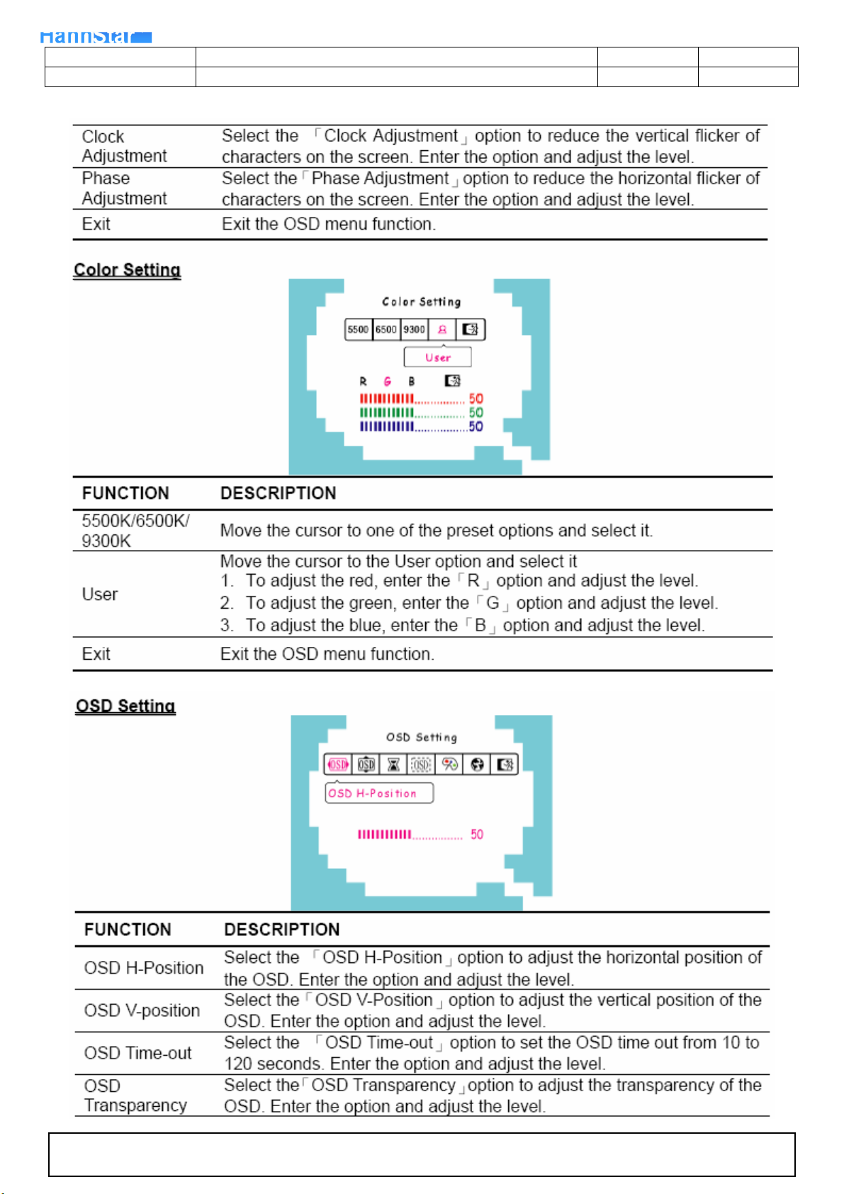
13. White- Balance, Luminance Adjustment
Approximately 30 minutes should be allowed for warm up before proceeding White-Balance adjustment.
1. How to do the Chroma-7120 MEM. Channel setting
A. Reference to chroma 7120 user guide
B. Use “SC” key and “NEXT” key to modify x,y,Y value and use “ID” key to modify the
TEXT description Following is the procedure to do white-balance adjust
2. Setting the color temp. you want
A. MEM.CHANNEL 3 (9300 color):
9300 color temp. parameter is x = 283 ±28, y = 297 ±28,Y=220cd/㎡
B. MEM.CHANNEL 4 (6500 color):
6500 color temp. parameter is x = 313±28, y = 329 ±28, Y=220cd/㎡
C. MEM.CHANNEL 9 (5500 color):
5500 color temp. parameter is x = 333±28, y = 348 ±28, Y=220cd/㎡
3. Enter into factory mode of HG171A:
Turn on the power, press simultaneously the MENU and AUTO buttons, then the factory OSD will be at the left top of the
panel.
4. Bias adjustment:
Set the Contrast ZHAN to 50; Adjust the Brightness
to 80.
5. Gain adjustment:
Move cursor to “-F-” and press MENU key
A. Adjust 9300 color-temperature
1. Switch the Chroma-7120 to RGB-Mode (with press “MODE” button)
2. Switch the MEM. Channel to Channel 3 (with up or down arrow on chroma 7120)
3. The LCD-indicator on chroma 7120 will show x = 283 ±28, y = 297 ±28, Y=220cd/㎡
4. Adjust the RED of color 1 on factory window until chroma 7120 indicator reached the value R=100
5. Adjust the GREEN of color 1 on factory window until chroma 7120 indicator reached the value G=100
6. Adjust the BLUE of color 1 on factory window until chroma 7120 indicator reached the value B=100
7. Repeat above procedure (item 4,5,6) until chroma 7120 RGB value meet the tolerance =100±2
B. Adjust 6500 color-temperature
1. Switch the chroma-7120 to RGB-Mode (with press “MODE” button)
2. Switch the MEM.channel to Channel 4(with up or down arrow on chroma 7120)
3. The LCD-indicator on chroma 7120 will show x = 313 ±28, y = 329 ±28, Y=220cd/㎡
4. Adjust the RED of color 2 on factory window until chroma 7120 indicator reached the value R=100
5. Adjust the GREEN of color 2 on factory window until chroma 7120 indicator reachedthe value G=100
6. Adjust the BLUE of color 2 on factory window until chroma 7120 indicator reached the value B=100
7. Repeat above procedure (item 4,5,6) until chroma 7120 RGB value meet the tolerance =100±2
C. Adjust 5500 color-temperature
The information contained in this document is the exclusive property of HannStar Display Corporation. It shall not be
disclosed,distributed or reproduced in whole or in part without written permission of HannStar Display Corporation.
Page 54

H a n n S t a r D i s p l a y C o r p .
Document Title HG171A_XY _HSM Page No.
Document No.
Revision
1. Switch the chroma-7120 to RGB-Mode (with press “MODE” button)
2. Switch the MEM.channel to Channel 9 (with up or down arrow on chroma 7120)
3. The LCD-indicator on chroma 7120 will show x = 333±28, y = 348 ±28, Y=220cd/㎡
4. Adjust the RED of color 3 on factory window until chroma 7120 indicator reached the value R=100
5. Adjust the GREEN of color 3 on factory window until chroma 7120 indicator reachedthe value G=100
6. Adjust the BLUE of color 3 on factory window until chroma 7120 indicator reached the value B=100
7. Repeat above procedure (item 4,5,6) until chroma 7120 RGB value meet the tolerance =100±2
D. Turn the Power-button off to quit from factory mode.
54 54 /65
08/09/09
The information contained in this document is the exclusive property of HannStar Display Corporation. It shall not be
disclosed,distributed or reproduced in whole or in part without written permission of HannStar Display Corporation.
Page 55

H a n n S t a r D i s p l a y C o r p .
Document Title HG171A_XY _HSM Page No.
Document No.
14.Monitor Exploded View
Revision
55 55 /65
08/09/09
Item Description Item Description
1 POWER LENS 14 HINGE
2 BEZEL 15 STAND FRONT
3 LOGO 16 STAND BACK
4 PANEL 17 BASE
5 POWER BOARD 18 PORON FOOT
6 MAIN BOARD S1 SCREW
7 MAIN FRAME S2 SCREW
8 KEYPAD S3 SCREW
9 KEY BOARD S4 SCREW
10 MYLAR S5 SCREW
11 SPENKER S6 SCREW
12 BACK COVER S7 SCREW
13 HINGE COVER S8 SCREW
The information contained in this document is the exclusive property of HannStar Display Corporation. It shall not be
disclosed,distributed or reproduced in whole or in part without written permission of HannStar Display Corporation.
Page 56

H a n n S t a r D i s p l a y C o r p .
Document Title HG171A_XY _HSM Page No.
Document No.
Revision
56 56 /65
08/09/09
15. BOM List
T7RHM5D8AWHZNC
Location Part NO. Description Remark
050G 600 1 W WHITE STRAP
050G 600 2 HANDLE1
050G 600 3 HANDLE2
052G 1150 C INSULATING TAPE
052G 1185 MIDDLE TAPE
052G 1186 SMALL TAPE
052G 1211 A Conductive Tape 55mm *45mm *0.08mm
052G 1211 B Conductive Tape 85mm *40mm *0.09mm
052G 1211527 Conductive Tape 75mm *45mm *0.08mm
052G6019 1 INSULATING TAPE
E08902 089G 725GAA DB D-SUB CABLE 2nd source
E08902 089G 725HAA DB D-SUB CABLE
E08907 089G179J30N504 ffc cable
E08907 089G179J30N504 ffc cable 2nd source
E08901 089G404A18N IS POWER CORD/32E1818018
E08901 089G404A18N YH POWER CORD(32E1818018/32-D022217) 2nd source
095G8014 6XH19 WIRE HARNESS 6P(1253HA HR)-6P(PH)
0M1G 130 5120 SCREW
0M1G 330 5225 CR3 SCREW
0M1G1730 6120 SCREW,42-D020523
0M1G1740 10120 SCREW 42A9940008
705GQ734421 REAR COVER/STAND ASS'Y(17")
0M1G1030 6120 SCREW M3X6
0Q1G 330 6120 SCREW 42A9930001
0Q1G1030 6120 SCREW
Q12G6600 8 PORON FOOT
Q33G0071 ZT 1L KEY PAD
Q34G0158 ZT 2B REAR COVER(17")
Q34G0160 ZT 1B STAND-F
Q34G0161 ZT 1B STAND-B
Q34G0162 ZT 1B 33 BASE
Q37G0046 1 HINGE
750GLH70GWB12N000R PANEL HSD170MGW1 B00 NJ HSD
756GQ8CB HZ001 MAIN BOARD-CBPCRM5HZQ2
SMTC-U402 100GTMH7000N11 MCU ASS'Y-056G1133 81
A15G0207HSD 3 MAIN FRAME
040G 45762412B CBPC LABEL
CN401 033G3802 6 WAFER
CN404 033G3802 9 WAFER 9P RIGHT ANELE PITCH
CN403 033G801930F CH JS CONNECTOR
The information contained in this document is the exclusive property of HannStar Display Corporation. It shall not be
disclosed,distributed or reproduced in whole or in part without written permission of HannStar Display Corporation.
Page 57

H a n n S t a r D i s p l a y C o r p .
Document Title HG171A_XY _HSM Page No.
Document No.
Revision
CN101 088G 35315F H D-SUB 15PIN
X401 093G 22 53 H 14.31818MHZ/30PF/49US
X401 093G 22 53 J 14.31818MHZ/32PF/49US
C410 067G 4051007PB EC 10uF M 50V 5*11mm
C426 067G 4051014PB EC 100uF M 25V 6.3*11mm
C427 067G 4051014PB EC 100uF M 25V 6.3*11mm
C421 067G 4051014PB EC 100uF M 25V 6.3*11mm
C423 067G 4051014PB EC 100uF M 25V 6.3*11mm
U401 056G 562557 IC TSUM1PFR-LF
U404 056G 563 52 IC AP1117D33L-13 TO252-3L DIODES
U103 056G 662 13 IC AZC099-04S SOT23-6L
U102 056G 662 13 IC AZC099-04S SOT23-6L
Q409 057G 417 22 T TRA KN2907AS -60V/-0.6A SOT-23
Q410 057G 417 22 T TRA KN2907AS -60V/-0.6A SOT-23
Q404 057G 417517 LMBT3906LT1G SOT-23 BY LRC
Q408 057G 417518 LMBT3904LT1G SOT-23 BY LRC
Q406 057G 417518 LMBT3904LT1G SOT-23 BY LRC
Q401 057G 763 1 A03401 SOT23 BY AOS(A1)
Q405 057G 763 1 A03401 SOT23 BY AOS(A1)
R456 061G0402000 RST CHIPR 0 OHM +-5% 1/16W
R402 061G0402000 RST CHIPR 0 OHM +-5% 1/16W
R401 061G0402000 RST CHIPR 0 OHM +-5% 1/16W
R457 061G0402000 RST CHIPR 0 OHM +-5% 1/16W
R102 061G0402101 RST CHIPR 100 OHM +-5% 1/16W
R103 061G0402101 RST CHIPR 100 OHM +-5% 1/16W
R104 061G0402101 RST CHIPR 100 OHM +-5% 1/16W
R108 061G0402101 RST CHIPR 100 OHM +-5% 1/16W
R110 061G0402101 RST CHIPR 100 OHM +-5% 1/16W
R111 061G0402101 RST CHIPR 100 OHM +-5% 1/16W
R113 061G0402101 RST CHIPR 100 OHM +-5% 1/16W
R442 061G0402101 RST CHIPR 100 OHM +-5% 1/16W
R420 061G0402101 RST CHIPR 100 OHM +-5% 1/16W
R419 061G0402101 RST CHIPR 100 OHM +-5% 1/16W
R418 061G0402101 RST CHIPR 100 OHM +-5% 1/16W
R413 061G0402101 RST CHIPR 100 OHM +-5% 1/16W
R412 061G0402101 RST CHIPR 100 OHM +-5% 1/16W
R411 061G0402101 RST CHIPR 100 OHM +-5% 1/16W
R405 061G0402101 RST CHIPR 100 OHM +-5% 1/16W
R117 061G0402101 RST CHIPR 100 OHM +-5% 1/16W
R115 061G0402101 RST CHIPR 100 OHM +-5% 1/16W
R114 061G0402101 RST CHIPR 100 OHM +-5% 1/16W
R441 061G0402102 RST CHIPR 1 KOHM +-5% 1/16W
R118 061G0402102 RST CHIPR 1 KOHM +-5% 1/16W
R408 061G0402103 RST CHIPR 10 KOHM +-5% 1/16W
57 57 /65
08/09/09
The information contained in this document is the exclusive property of HannStar Display Corporation. It shall not be
disclosed,distributed or reproduced in whole or in part without written permission of HannStar Display Corporation.
Page 58

H a n n S t a r D i s p l a y C o r p .
Document Title HG171A_XY _HSM Page No.
Document No.
Revision
R409 061G0402103 RST CHIPR 10 KOHM +-5% 1/16W
R417 061G0402103 RST CHIPR 10 KOHM +-5% 1/16W
R421 061G0402103 RST CHIPR 10 KOHM +-5% 1/16W
R433 061G0402103 RST CHIPR 10 KOHM +-5% 1/16W
R437 061G0402103 RST CHIPR 10 KOHM +-5% 1/16W
R439 061G0402103 RST CHIPR 10 KOHM +-5% 1/16W
R447 061G0402103 RST CHIPR 10 KOHM +-5% 1/16W
R121 061G0402103 RST CHIPR 10 KOHM +-5% 1/16W
R404 061G0402103 RST CHIPR 10 KOHM +-5% 1/16W
R407 061G0402103 RST CHIPR 10 KOHM +-5% 1/16W
R120 061G0402103 RST CHIPR 10 KOHM +-5% 1/16W
R436 061G0402104 RST CHIPR 100 KOHM +-5% 1/16W
R410 061G0402121 RST CHIP 120R 1/16W 5%
R414 061G0402121 RST CHIP 120R 1/16W 5%
R458 061G0402203 RST CHIP 20K 1/16W 5%
R105 061G0402222 RST CHIPR 2.2 KOHM +-5% 1/16W
R106 061G0402222 RST CHIPR 2.2 KOHM +-5% 1/16W
R459 061G0402303 RST CHIPR 30 KOHM +-5% 1/16W
R109 061G0402390 0F RST CHIP 390R 1/16W 1%
R403 061G0402390 0F RST CHIP 390R 1/16W 1%
R427 061G0402392 RST CHIP 3.9K 1/16W 5%
R428 061G0402392 RST CHIP 3.9K 1/16W 5%
R435 061G0402472 RST CHIPR 4.7 KOHM +-5% 1/16W
R440 061G0402472 RST CHIPR 4.7 KOHM +-5% 1/16W
R448 061G0402472 RST CHIPR 4.7 KOHM +-5% 1/16W
R406 061G0402682 RST CHIP 6K8 1/16W 5%
R107 061G0402750 RST CHIPR 75 OHM +-5% 1/16W
R112 061G0402750 RST CHIPR 75 OHM +-5% 1/16W
R116 061G0402750 RST CHIPR 75 OHM +-5% 1/16W
R101 061G0603000 RST CHIPR 0 OHM +-5% 1/10W
R434 061G1206331 RST CHIPR 330 OHM +-5% 1/4W
C432 065G0402104 15 MLCC 0402 0.1UF K 16V X5R
C428 065G0402104 15 MLCC 0402 0.1UF K 16V X5R
C422 065G0402104 15 MLCC 0402 0.1UF K 16V X5R
C420 065G0402104 15 MLCC 0402 0.1UF K 16V X5R
C419 065G0402104 15 MLCC 0402 0.1UF K 16V X5R
C417 065G0402104 15 MLCC 0402 0.1UF K 16V X5R
C416 065G0402104 15 MLCC 0402 0.1UF K 16V X5R
C415 065G0402104 15 MLCC 0402 0.1UF K 16V X5R
C414 065G0402104 15 MLCC 0402 0.1UF K 16V X5R
C413 065G0402104 15 MLCC 0402 0.1UF K 16V X5R
C409 065G0402104 15 MLCC 0402 0.1UF K 16V X5R
C407 065G0402104 15 MLCC 0402 0.1UF K 16V X5R
C406 065G0402104 15 MLCC 0402 0.1UF K 16V X5R
58 58 /65
08/09/09
The information contained in this document is the exclusive property of HannStar Display Corporation. It shall not be
disclosed,distributed or reproduced in whole or in part without written permission of HannStar Display Corporation.
Page 59

H a n n S t a r D i s p l a y C o r p .
Document Title HG171A_XY _HSM Page No.
Document No.
Revision
C404 065G0402104 15 MLCC 0402 0.1UF K 16V X5R
C403 065G0402104 15 MLCC 0402 0.1UF K 16V X5R
C401 065G0402104 15 MLCC 0402 0.1UF K 16V X5R
C412 065G0402220 31 CHIP 22PF 50V NPO
C411 065G0402220 31 CHIP 22PF 50V NPO
C103 065G0402220 31 CHIP 22PF 50V NPO
C102 065G0402220 31 CHIP 22PF 50V NPO
C408 065G0402224 17 CAP CER 0.22UF -20%-80%
C113 065G0402473 12 CHIP 0.047uF 16V X7R
C110 065G0402473 12 CHIP 0.047uF 16V X7R
C109 065G0402473 12 CHIP 0.047uF 16V X7R
C107 065G0402473 12 CHIP 0.047uF 16V X7R
C106 065G0402473 12 CHIP 0.047uF 16V X7R
C105 065G0402473 12 CHIP 0.047uF 16V X7R
C101 065G0402473 12 CHIP 0.047uF 16V X7R
C111 065G0402509 31 CHIP 5pF 50V NPO
C104 065G0402509 31 CHIP 5pF 50V NPO
C108 065G0402509 31 CHIP 5pF 50V NPO
FB402 071G 56K121 M CHIP BEAD
FB401 071G 56V301 B CHIP BEAD FCM2012VF-301T07 bullwill
FB101 071G 59K190 B 19 OHM BEAD
FB102 071G 59K190 B 19 OHM BEAD
FB103 071G 59K190 B 19 OHM BEAD
D401 093G 64 33 DIO SIG SM BAV99 (PHSE)R
ZD103 093G 39S 34 T UDZSNP5.6B ROHM
ZD104 093G 39S 34 T UDZSNP5.6B ROHM
D402 093G3004 3 SM340A
715G2904 1 9 MAIN PCB 57x64x1.6mm DS
KEPC8QH2 KEY G2601-2-X-X-3-080815
CN101 033G8032 6F HR CONNECTOR
R103 061G0603182 RST CHIPR 1.8 KOHM +-5% 1/10W
R102 061G0603182 RST CHIPR 1.8 KOHM +-5% 1/10W
R104 061G0603302 RST CHIPR 3 KOHM +-5% 1/10W
R101 061G0603302 RST CHIPR 3 KOHM +-5% 1/10W
C111 065G0603104 32 CHIP 0.1UF 50V X7R
C110 065G0603104 32 CHIP 0.1UF 50V X7R
C109 065G0603104 32 CHIP 0.1UF 50V X7R
C108 065G0603104 32 CHIP 0.1UF 50V X7R
C107 065G0603104 32 CHIP 0.1UF 50V X7R
C106 065G0603104 32 CHIP 0.1UF 50V X7R
FB102 071G 56K121 M CHIP BEAD
SW104 077G 604 2 TO TACT 5W BY TOUKE TS-9-TMG-553
SW105 077G 604 2 TO TACT 5W BY TOUKE TS-9-TMG-553
SW103 077G 604 2 TO TACT 5W BY TOUKE TS-9-TMG-553
59 59 /65
08/09/09
The information contained in this document is the exclusive property of HannStar Display Corporation. It shall not be
disclosed,distributed or reproduced in whole or in part without written permission of HannStar Display Corporation.
Page 60

H a n n S t a r D i s p l a y C o r p .
Document Title HG171A_XY _HSM Page No.
Document No.
Revision
60 60 /65
SW101 077G 604 2 TO TACT 5W BY TOUKE TS-9-TMG-553
SW102 077G 604 2 TO TACT 5W BY TOUKE TS-9-TMG-553
LED101 081G 15502 GP LED GPTD12048YGC1
ZD101 093G 39S 34 T UDZSNP5.6B ROHM
ZD102 093G 39S 34 T UDZSNP5.6B ROHM
ZD103 093G 39S 34 T UDZSNP5.6B ROHM
ZD104 093G 39S 34 T UDZSNP5.6B ROHM
ZD105 093G 39S 34 T UDZSNP5.6B ROHM
ZD106 093G 39S 34 T UDZSNP5.6B ROHM
715G2601 1 2 KEY PCB FR-4 T1.2MM 112X12.3MM
PWPC8721HQFD POWER G2545-2-2-X-3-080821
040G 45762412B CBPC LABEL
GND1 009G6005 1 GROUND TERMINAL
CN802 033G8020 2D U WAFER 2nd source
CN801 033G8020 2D U WAFER 2nd source
CN801 033G8020 2E F CONNECTOR
CN802 033G8020 2E F CONNECTOR
IC903 056G 139 3A IC PC123Y22FZ0F
NR901 061G 58080 WT 8 OHM NCT
C903 063G107K474 US 0.47UF +-10%
C801 065G 6J1506ET 15PF 5% SL 6KV
C901 065G305M1022BP Y2 1000PF M 250VAC Y5P
C902 065G305M1022BP Y2 1000PF M 250VAC Y5P
C921 065G306M3322BP 3300PF 20%
C907 067G 40Z10115K
C802 067G215D4714KV
C918 067G215D6814KV
C917 067G215D6814KV
C940 067G215S1023KV
C939 067G215S1023KV
C915 067G215S4713KV
C922 067G215Y4714HV
CAP 105℃ 100UF M 450V
E.C 105℃ CAP 470UF M 25V ED SERIES
CAP 105℃ 680uF M 25V
CAP 105℃ 680uF M 25V
105℃ 1000UF M 16V
105℃ 1000UF M 16V
EC 105℃ CAP 470UF M 16V
EC 105℃ CAP 470UF M 25V
L902 073G 174 65 H LINE FILTER
T901 080GL17T 33 DN XFMR FOR POWER Darfon
CN901 087G 501 32 S AC SOCKET
BD901 093G 50460 28 BRIDGE DIODE KBP208G LITEON
CN902 095G801410D 51 HARNESS 10P-9P 110mm 2nd source
CN902 095G801410E 51 WIRE HARNESS
705GQ7 57001 Q901 ASS'Y
Q901 057G 724 11 STP9NK65ZFP
HS3 090G6263 1 HEAT SINK
0M1G1730 8120 SCREW
705GQ7 93001 D905 ASS'Y
HS4 090G6084 1 HEAT SINK
08/09/09
The information contained in this document is the exclusive property of HannStar Display Corporation. It shall not be
disclosed,distributed or reproduced in whole or in part without written permission of HannStar Display Corporation.
Page 61

H a n n S t a r D i s p l a y C o r p .
Document Title HG171A_XY _HSM Page No.
Document No.
Revision
D905 093G 60257 DIODE SB1060FCT ITO-220AB BY PAN JIT
0M1G1730 8120 SCREW
705GQ761006 R908 ASS'Y
R908 061G152M10458F 100K OHM 5% 2W
096G 29 6 H.S. TUBE
705GQ761007 R914 ASS'Y
R914 061G152M478 64 0.47 OHM 5% 2W
096G 29 1 SHRINK TUBE UL/CSA
705GQ793012 D906 ASS'Y
D906 093G 60218 SB10100FCT
0M1G1730 8120 SCREW
HS2 Q90G6263 2 HEAT SINK
IC801 056G 379 22 IC TL494IDR SOIC-16
IC901 056G 379 76 IC LD7552BPS SOP-8
Q903 057G 417 4 PMBS3904/PHILIPS-SMT(04)
Q811 057G 417 4 PMBS3904/PHILIPS-SMT(04)
Q806 057G 417 4 PMBS3904/PHILIPS-SMT(04)
Q801 057G 417 4 PMBS3904/PHILIPS-SMT(04)
Q804 057G 417 6 PMBS3906/PHILIPS-SMT(06)
Q812 057G 417 6 PMBS3906/PHILIPS-SMT(06)
Q809 057G 759 2 RK7002
Q810 057G 759 2 RK7002
Q808 057G 760 4B PDTA144WK SOT346
Q805 057G 760 5B PDTC144WK SOT346
Q802 057G 763 14 AM9945N
R823 061G0603000 RST CHIPR 0 OHM +-5% 1/10W
R801 061G0603100 1F RST CHIPR 1 KOHM +-1% 1/10W
R818 061G0603100 1F RST CHIPR 1 KOHM +-1% 1/10W
R824 061G0603100 1F RST CHIPR 1 KOHM +-1% 1/10W
R808 061G0603100 1F RST CHIPR 1 KOHM +-1% 1/10W
R814 061G0603100 1F RST CHIPR 1 KOHM +-1% 1/10W
R827 061G0603100 1F RST CHIPR 1 KOHM +-1% 1/10W
R926 061G0603100 1F RST CHIPR 1 KOHM +-1% 1/10W
R942 061G0603100 1F RST CHIPR 1 KOHM +-1% 1/10W
R807 061G0603100 2F RST CHIPR 10K OHM +-1% 1/10W
R817 061G0603100 2F RST CHIPR 10K OHM +-1% 1/10W
R820 061G0603100 2F RST CHIPR 10K OHM +-1% 1/10W
R828 061G0603100 2F RST CHIPR 10K OHM +-1% 1/10W
R832 061G0603100 2F RST CHIPR 10K OHM +-1% 1/10W
R863 061G0603100 2F RST CHIPR 10K OHM +-1% 1/10W
R813 061G0603102 RST CHIPR 1K OHM +-5% 1/10W
R862 061G0603105 RST CHIPR 1M OHM +-5% 1/10W
R835 061G0603105 RST CHIPR 1M OHM +-5% 1/10W
R803 061G0603106 RST CHIPR 10M OHM +-5% 1/10W
61 61 /65
08/09/09
The information contained in this document is the exclusive property of HannStar Display Corporation. It shall not be
disclosed,distributed or reproduced in whole or in part without written permission of HannStar Display Corporation.
Page 62

H a n n S t a r D i s p l a y C o r p .
Document Title HG171A_XY _HSM Page No.
Document No.
Revision
R930 061G0603243 1F RST CHIPR 2.43K OHM +-1% 1/10W
R940 061G0603330 2F RST CHIPR 33K OHM +-1% 1/10W
R927 061G0603360 1F RST CHIPR 3.6K OHM +-1% 1/10W
R802 061G0603470 1F RST CHIPR 4.7 KOHM +-1% 1/10W
R811 061G0603472 RST CHIPR 4.7K OHM +-5% 1/10W
R841 061G0603680 2F RST CHIPR 68K OHM +-1% 1/10W
R853 061G0603683 RST CHIPR 68K OHM +-5% 1/10W
R831 061G0805100 1F RST CHIPR 1K OHM +-1% 1/8W
R915 061G0805100 3F RST CHIPR 100KOHM +-1% 1/8W
R804 061G0805101 1ST CHIPR 100 OHM +-5% 1/8W
R925 061G0805102 RST CHIPR 1K OHM +-5% 1/8W
R826 061G0805102 RST CHIPR 1K OHM +-5% 1/8W
R943 061G0805102 RST CHIPR 1K OHM +-5% 1/8W
R938 061G0805103 RST CHIPR 10K OHM +-5% 1/8W
R924 061G0805151 RST CHIPR 150 OHM +-5% 1/8W
R829 061G0805220 RST CHIPR 22 OHM +-5% 1/8W
R825 061G0805220 RST CHIPR 22 OHM +-5% 1/8W
R839 061G0805220 RST CHIPR 22 OHM +-5% 1/8W
R850 061G0805220 RST CHIPR 22 OHM +-5% 1/8W
R837 061G0805473 RST CHIPR 47K OHM +-5% 1/8W
R810 061G0805510 2F RST CHIPR 51K OHM +-1% 1/8W
F801 061G1206000 RST CHIPR 0 OHM +-5% 1/4W
JR801 061G1206000 RST CHIPR 0 OHM +-5% 1/4W
JR901 061G1206000 RST CHIPR 0 OHM +-5% 1/4W
JR902 061G1206000 RST CHIPR 0 OHM +-5% 1/4W
R910 061G1206100 RST CHIPR 10 OHM +-5% 1/4W
R821 061G1206100 1F RST CHIPR 1K OHM +-1% 1/4W
R822 061G1206100 1F RST CHIPR 1K OHM +-1% 1/4W
R918 061G1206101 RST CHIPR 100 OHM +-5% 1/4W
R919 061G1206101 RST CHIPR 100 OHM +-5% 1/4W
R920 061G1206101 RST CHIPR 100 OHM +-5% 1/4W
R935 061G1206101 RST CHIPR 100 OHM +-5% 1/4W
R961 061G1206101 RST CHIPR 100 OHM +-5% 1/4W
R962 061G1206101 RST CHIPR 100 OHM +-5% 1/4W
R946 061G1206102 RST CHIPR 1k OHM +-5% 1/4W
R945 061G1206102 RST CHIPR 1k OHM +-5% 1/4W
R944 061G1206102 RST CHIPR 1k OHM +-5% 1/4W
R941 061G1206102 RST CHIPR 1k OHM +-5% 1/4W
R912 061G1206221 RST CHIPR 220 OHM +-5% 1/4W
R904 061G1206304 RST CHIPR 300k OHM +-5% 1/4W
R933 061G1206304 RST CHIPR 300k OHM +-5% 1/4W
R932 061G1206304 RST CHIPR 300k OHM +-5% 1/4W
R855 061G1206330 RST CHIPR 33 OHM +-5% 1/4W
R856 061G1206330 RST CHIPR 33 OHM +-5% 1/4W
62 62 /65
08/09/09
The information contained in this document is the exclusive property of HannStar Display Corporation. It shall not be
disclosed,distributed or reproduced in whole or in part without written permission of HannStar Display Corporation.
Page 63

H a n n S t a r D i s p l a y C o r p .
Document Title HG171A_XY _HSM Page No.
Document No.
Revision
R909 061G1206519 RST CHIPR 5.1 OHM +-5% 1/4W
R900 061G1206684 RST CHIPR 680K OHM +-5% 1/4W
R901 061G1206684 RST CHIPR 680K OHM +-5% 1/4W
R902 061G1206684 RST CHIPR 680K OHM +-5% 1/4W
C842 065G0603103 32 CAP CHIP 0603 0.01UF K 50V X7R
C807 065G0603104 22 CAP CHIP 0603 0.1UF K 25V X7R
C821 065G0603104 22 CAP CHIP 0603 0.1UF K 25V X7R
C825 065G0603104 22 CAP CHIP 0603 0.1UF K 25V X7R
C834 065G0603104 22 CAP CHIP 0603 0.1UF K 25V X7R
C819 065G0603222 22 CHIP 2200PF 25V X7R
C823 065G0603222 22 CHIP 2200PF 25V X7R
C932 065G0805102 31 CAP CHIP 0805 1000PF J 50V NPO
C839 065G0805102 31 CAP CHIP 0805 1000PF J 50V NPO
C838 065G0805102 31 CAP CHIP 0805 1000PF J 50V NPO
C928 065G0805103 32 CAP CHIP 0805 10NF K 50V X7R
C930 065G0805104 32 CAP CHIP 0805 0.1uF K 50V X7R
C924 065G0805104 32 CAP CHIP 0805 0.1uF K 50V X7R
C916 065G0805104 32 CAP CHIP 0805 0.1uF K 50V X7R
C905 065G0805104 32 CAP CHIP 0805 0.1uF K 50V X7R
C824 065G0805104 32 CAP CHIP 0805 0.1uF K 50V X7R
C845 065G0805105 22 CAP CHIP 0805 1uF K 25V X7R
C822 065G0805105 22 CAP CHIP 0805 1uF K 25V X7R
C820 065G0805221 31 CAP CHIP 0805 220PF J 50V NPO
C909 065G0805471 21 CAP CHIP 0805 470PF J 25V NPO
C912 065G1206102 72 CAP CHIP 1206 1000PF K 500V X7R
C929 065G1206102 72 CAP CHIP 1206 1000PF K 500V X7R
D805 093G 6432S 1N4148W
D806 093G 6432S 1N4148W
D807 093G 6432S 1N4148W
D812 093G 6432S 1N4148W
D813 093G 6432S 1N4148W
D814 093G 6432S 1N4148W
D817 093G 6432S 1N4148W
D903 093G 6432S 1N4148W
D915 093G 6432S 1N4148W
D916 093G 6432S 1N4148W
D802 093G 6433P BAV99
D801 093G 6433P BAV99
ZD801 093G 39S 10 T RLZ6.8B BY ROHM
ZD906 093G 39S 20 T RLZ22B LLDS
ZD922 093G 39S 25 T RLZ5.1B LLDS
ZD902 093G 39S 40 T RLZ 13B LLDS
ZD921 093G 39S 40 T RLZ 13B LLDS
ZD905 093G 39S 44 T RLZ18B LLDS
63 63 /65
08/09/09
The information contained in this document is the exclusive property of HannStar Display Corporation. It shall not be
disclosed,distributed or reproduced in whole or in part without written permission of HannStar Display Corporation.
Page 64

H a n n S t a r D i s p l a y C o r p .
Document Title HG171A_XY _HSM Page No.
Document No.
Revision
CN901 006G 31500 EYELET
T901 006G 31502 1.5MM RIVET
IC904 056G 158 12 KIA431A-AT/P TO-92
C938 065G 1K152 1T 1.5NF/1KV Z5F+-10%
C906 065G 2K152 1T GP CERAMIC CAP
C908 067G215Y2207KT
CAP 105℃ 22UF M 50V KINGNICHI
FB801 071G 55 9 T FERRITE BEAD
FB901 071G 55 29 FERRITE BEAD
F901 084G 55 7W FUSE 3.15A 250V Wickmann
F903 084G 56 4W FUSE 4.0A 250V
D900 093G 6026T52T RECTIFIER DIODE FR107
D901 093G 6038T52T FR103
715G2545 2 2 POWER-PCB FR-1 193x124x1.6MM SS
L901 S73G17476V LINE FILTER ASS'Y
L903 S73G25391V1 CHOKE COIL ASS'Y
L904 S73G25391V1 CHOKE COIL ASS'Y
Q34FPE19P06 CASE EEL19
071FPE19301 02 FP2 EEL19 01
Q05G6069 1 WASHER
Q23G3178850 1A LOGO
Q33G0072 Y 1X POWER LENS
Q34G0157 ASA1B 30 BEZEL L17W06A-hanns2
Q34G0159 ZT 1B HINGE COVER
Q44G7048 1 EPS
Q44G7048 2 EPS
Q44G7048 3EPE EPE
Q44G7048624 1A CARTON
Q45G 77 5 PE PACKING
Q45G 88607 35 PE BAG FOR BASE
Q45G 88609102 EPE BAG FOR MONITOR
Q52G6020 44 PROTECT FILM
64 64 /65
08/09/09
The information contained in this document is the exclusive property of HannStar Display Corporation. It shall not be
disclosed,distributed or reproduced in whole or in part without written permission of HannStar Display Corporation.
Page 65

H a n n S t a r D i s p l a y C o r p .
Document Title HG171A_XY _HSM Page No.
Document No.
16. Different Parts List
Diversity of T7RHM5DBAWZ3NN compared with T7RHM5D8AWHZNC
Location Part No. Description Remark
089G410A18N IS POWER CORD 32E1818020
E09502 095G8014 6DH39 HARNESS 6P(A1253HA HR)-6P(PH) 300mm 2nd source
E09502 095G8014 6XH39 HARNESS 6P(A1253HA HR)-6P(PH) 300mm
E750 750GLH70GWB12M000R PANEL HSD170MGW1 B00 NJ HSD
E750 750GLH70GWB1WM000R PANEL HSD170MGW1-B00 WH HSD 2nd source
Q40G 58170931A HT POT LABEL
Q40G000260811A Basic label
Q40G0002850 2A EPA LABEL
Q40G0002850 3A Seal label
Q44G7048850 4A 17"LCD CARTON
Q45G 76 28A32 PE BAG
E08907 S89G179T30N504 LVDS ASSY
089F80002203AG 1.0*30*2.5-220-3-0.65*0.05
033F303FH10BK3 F1010HA-30P-BK
033F303FJSHK30 1.0S-19-30A
044F3231 167C7 30*11.5*0.1
044F3231 167C2 SEKISUI5760#W=25
044F3231 167C4 5760 EVA (30*10*0.8mm)
Q41G780085016C warranty card
Q41G780085030A QSG(HG171A)
Q70G7008850 7A CD MANUAL(HG171A)
040G 58162435A P/N LABEL FOR MANUAL PE BAG
P40GD000813 9A FAMILY SHEET
Revision
65 65 /65
08/09/09
The information contained in this document is the exclusive property of HannStar Display Corporation. It shall not be
disclosed,distributed or reproduced in whole or in part without written permission of HannStar Display Corporation.
 Loading...