

Page 1
HannStar Display Corp.
The information contained in this document is the exclusive property of HannStar Display Corporation. It shall not
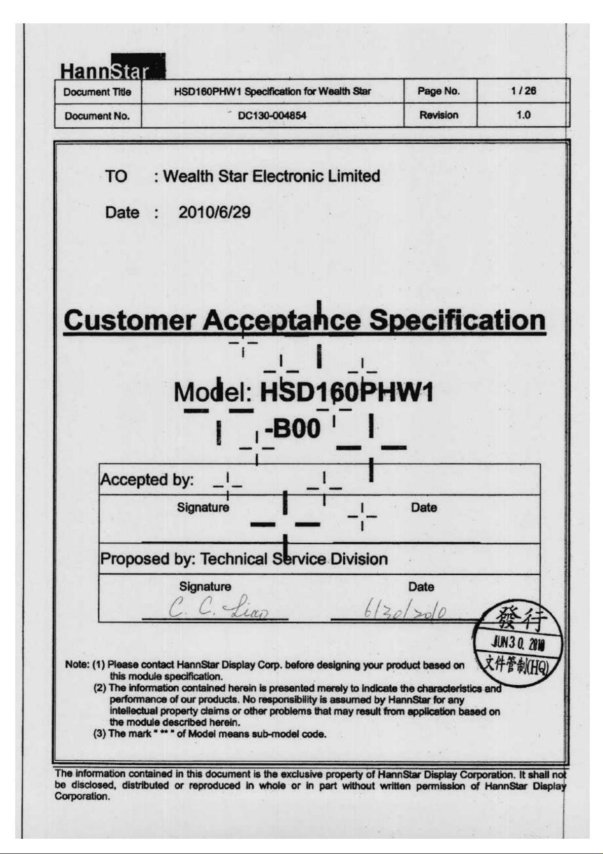
Document Title HSD160PHW1 Specification for Wealth Star Page No. 1/26
Document No. DC130-004854 Revision 1.0
TO : Wealth Star Electronic Limited
Date : 2010/6/29
Customer Acceptance Specification
Model: HSD160PHW1
-B00
Accepted by:
Proposed by: Technical Service Division
Signature Date
Note: (1) Please contact HannStar Display Corp. before designing your product based on
this module specification.
(2) The information contained herein is presented merely to indicate the characteristics and
performance of our products. No responsibility is assumed by HannStar for any
intellectual property claims or other problems that may result from application based on
the module described herein.
(3) The mark “ ** ” of Model means sub-model code.
Signature Date
be disclosed, distributed or reproduced in whole or in part without written permission of HannStar Display
Corporation.
Page 2
HannStar Display Corp.
The information contained in this document is the exclusive property of HannStar Display Corporation. It shall not
Document Title HSD160PHW1 Specification for Wealth Star Page No. 2/26
Document No. DC130-004854 Revision 1.0
Record of Revisions
Rev.
Date Sub-Model
2010/6/29
B00 Formal Product Specification was first released.
Description of change
be disclosed, distributed or reproduced in whole or in part without written permission of HannStar Display
Corporation.
Page 3
HannStar Display Corp.
The information contained in this document is the exclusive property of HannStar Display Corporation. It shall not
Document Title HSD160PHW1 Specification for Wealth Star Page No. 3/26
Document No. DC130-004854 Revision 1.0
Contents
1.0 General description ………………………………… p.4
2.0 Absolute maximum ratings……………………………. p.5
3.0 Optical characteristics.………………………………. p.6
4.0 Block diagram ……………………………………… p.10
5.0 Interface pin connection …………………………… p.12
6.0 Electrical characteristics …………………………… p.13
7.0 Reliability test items ………………………………… p.20
8.0 Outline dimension …………………………………… p.21
9.0 Lot mark ……………………………………………... p.23
10.0 Package specification ……………………………… p.24
11.0 General precaution …………………………………… p.25
be disclosed, distributed or reproduced in whole or in part without written permission of HannStar Display
Corporation.
Page 4
HannStar Display Corp.
The information contained in this document is the exclusive property of HannStar Display Corporation. It shall not
Document Title HSD160PHW1 Specification for Wealth Star Page No. 4/26
Document No. DC130-004854 Revision 1.0
1.0 GENERAL DESCRIPTION
1.1 Introduction
HannStar Display model HSD160PHW1-B is a color active matrix thin film
transistor (TFT) liquid crystal display (LCD) that uses amorphous silicon TFT as a
switching device. This model is composed of a TFT LCD panel, a driving circuit
and a back light system. This TFT LCD has a 16 (16:9) inch diagonally measured
active display area with HD (1366 horizontal by 768 vertical pixel) resolution.
1.2 Features
■ 16 (16:9 diagonal) inch configuration
■ One channel LVDS interface
■ 262K color by 6 bit R.G.B signal input
■ RoHS Compliance
■ Halogen Free
1.3 Applications
NB
1.4 General information
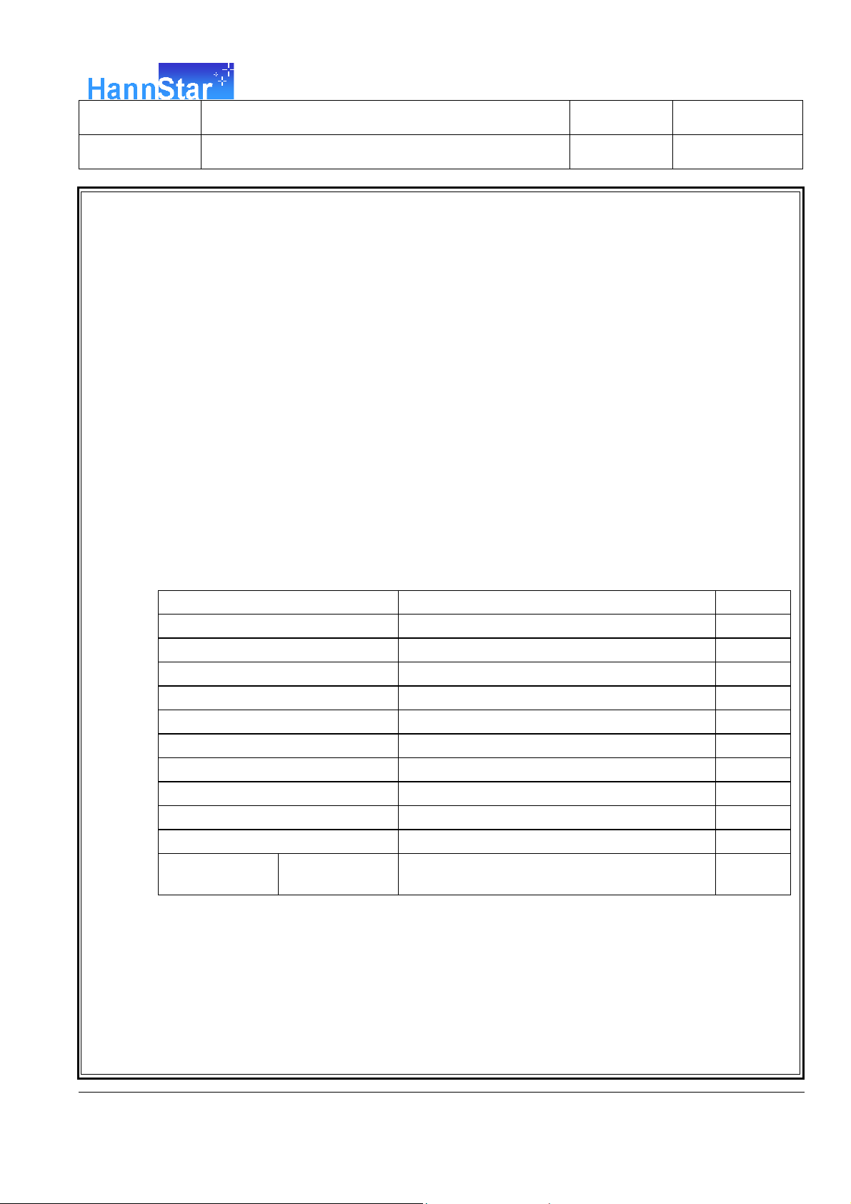
Item Specification Unit
Outline Dimension 365 x 214 x 5.5 (Typ.) mm
Display area 353.45(H) x 198.72(V) mm
Number of Pixel 1366 RGB (H) x 768(V) pixels
Pixel pitch 0.2587(H) x 0.2587(V) mm
Pixel arrangement RGB Vertical stripe
Display mode Normally white
NTSC 60 %
Surface treatment Glare, Hard-Coating (3H)
Weight 450 (Typ.) g
Back-light White LED
Power
Consumption
Logic System 1.2 (Max.) L0 pattern W
be disclosed, distributed or reproduced in whole or in part without written permission of HannStar Display
Corporation.
Page 5
HannStar Display Corp.
The information contained in this document is the exclusive property of HannStar Display Corporation. It shall not
Document Title HSD160PHW1 Specification for Wealth Star Page No. 5/26
Document No. DC130-004854 Revision 1.0
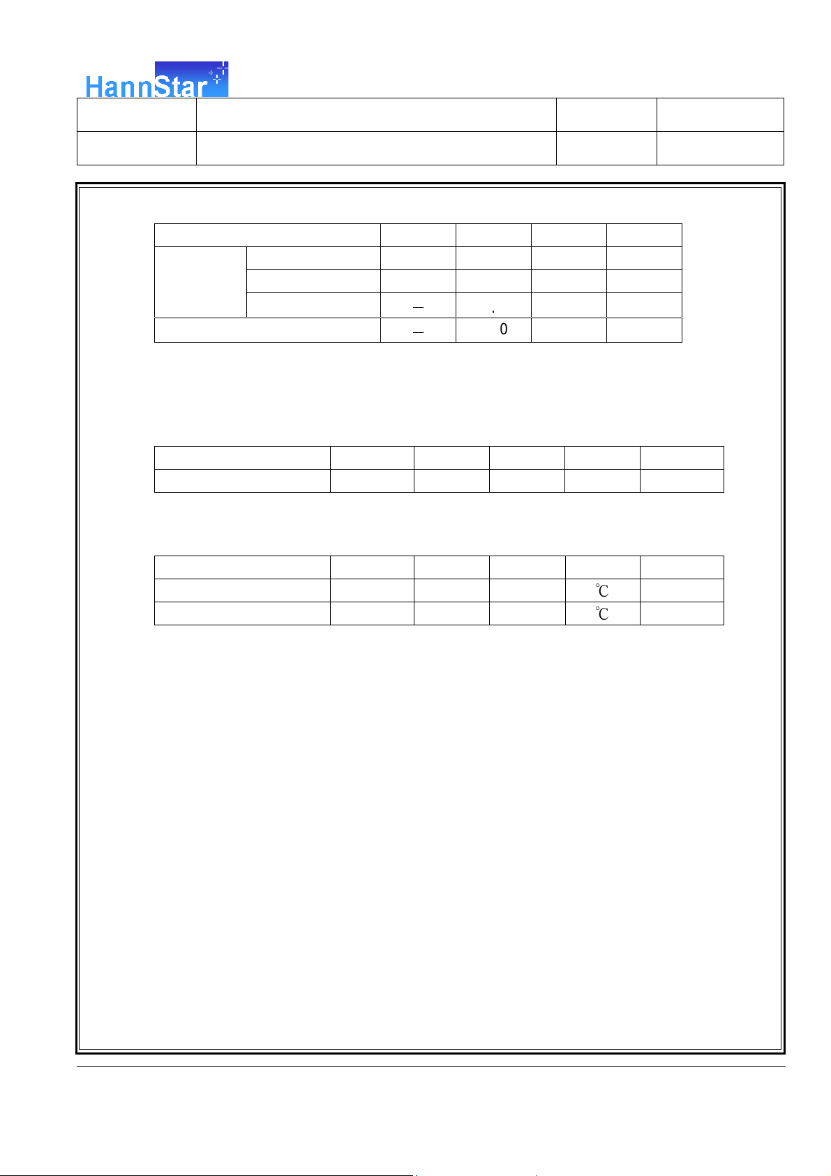
1.5 Mechanical Information
Item Min. Typ. Max. Unit
Horizontal (H) 364.5 365 365.5 mm
Module
Size
Weight
Vertical (V) 213.5 214 214.5 mm
Depth (D)
-
-
5.5
450 465 g
5.8 mm
2.0 ABSOLUTE MAXIMUM RATINGS
2.1 Electrical Absolute Rating
2.1.1 TFT LCD Module
Item Symbol Min. Max. Unit Note
Logic Supply voltage
2.1.2 Environment Absolute Rating
Item Symbol Min. Max. Unit Note
Operating Temperature T
Storage Temperature T
VDD -0.3 4.0 V
0 50
opa
-20 60
stg
℃
℃
be disclosed, distributed or reproduced in whole or in part without written permission of HannStar Display
Corporation.
Page 6
HannStar Display Corp.
The information contained in this document is the exclusive property of HannStar Display Corporation. It shall not
Document Title HSD160PHW1 Specification for Wealth Star Page No. 6/26
Document No. DC130-004854 Revision 1.0
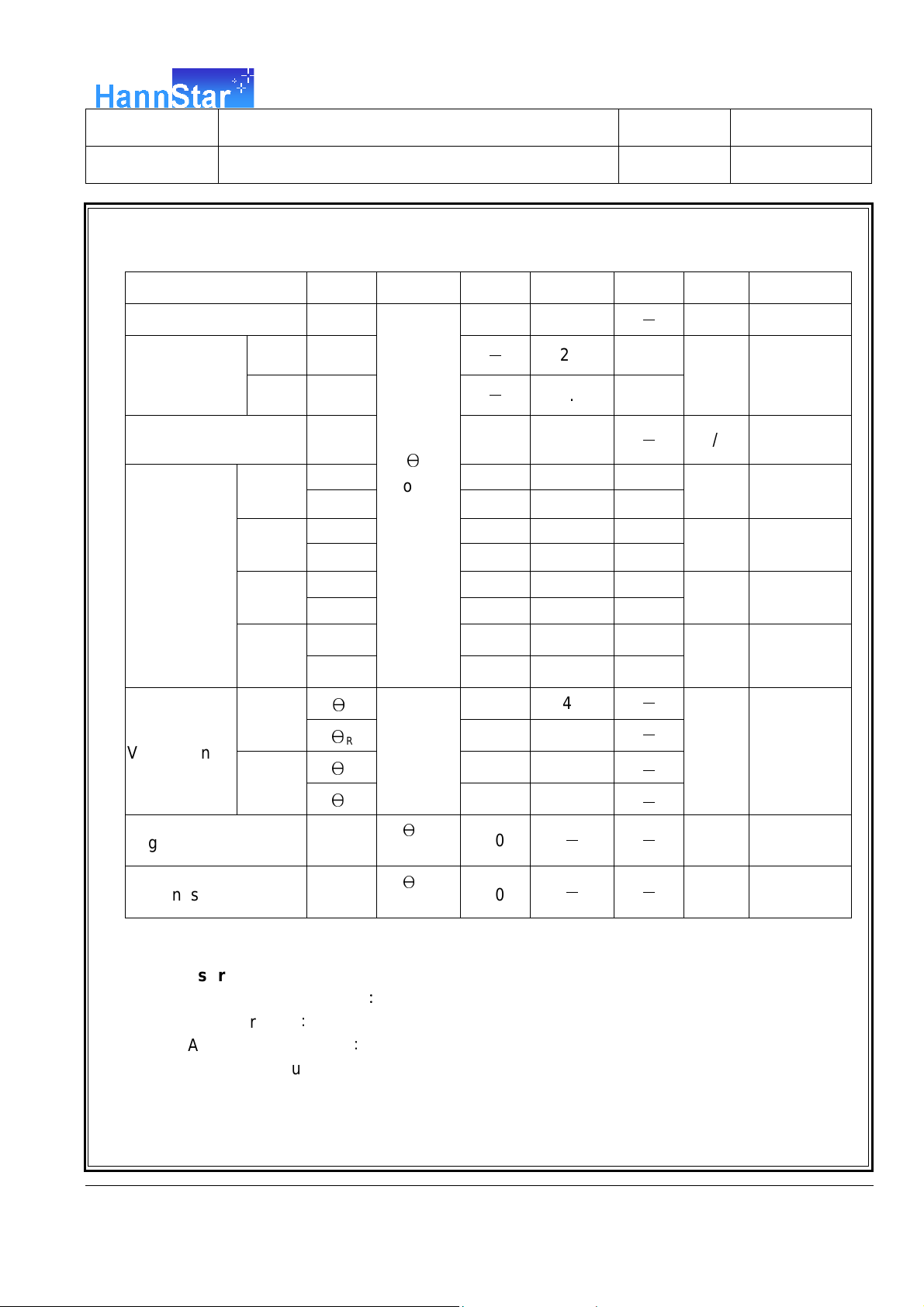
3.0 OPTICAL CHARACTERISTICS
3.1 Optical specification
Item Symbol Condition Min. Typ. Max. Unit Note
-
Contrast CR
Rising
Tr
Response time
Falling
Tf
480 600
-
-
2.4 4.8
5.6 11.2
(1)(2)(4)
msec
(1)(3)
White luminance
(5 point)
Red
Color
Green
chromaticity
(CIE1931)
Blue
White
Hor.
Viewing angle
Ver.
Brightness uniformity B
Brightness Uniformity B
3.2 Measuring Condition
■ Measuring surrounding:dark room
■ LED current I
■ Ambient temperature:25±2oC
■ 15min. warm-up time.
YL 176 220
Θ=0
Rx
RY
Gx
GY
Bx
BY
Wx
Wy
Θ
Θ
L
R
Normal
viewing
angle
0.584
0.312
0.318
0.582
0.120
0.039
0.283
0.299
40 45
40 45
CR>10
Θ
U
Θ
D
UNI
UNI
:
15mA / single LED
L
(5point)
(13 points)
Θ
Θ
=0
=0
10 15
30 35
80
70
-
0.614
0.342
0.348
0.612
0.150
0.069
0.644
0.372
0.378
0.642
0.180
0.099
0.313 0.343
0.329 0.359
-
-
-
-
-
-
-
-
(1)(4)(5)
2
cd/m
(IL=15mA)
(1)(4)
% (6)
% (6)
be disclosed, distributed or reproduced in whole or in part without written permission of HannStar Display
Corporation.
Page 7
HannStar Display Corp.
The information contained in this document is the exclusive property of HannStar Display Corporation. It shall not
o
Document Title HSD160PHW1 Specification for Wealth Star Page No. 7/26
Document No. DC130-004854 Revision 1.0
3.3 Measuring Equipment
■ FPM520 of Westar Display technologies, INC., which utilized SR-3 for Chromaticity
and BM-5A for other optical characteristics.
■ Measuring spot size:20 ~ 21 mm
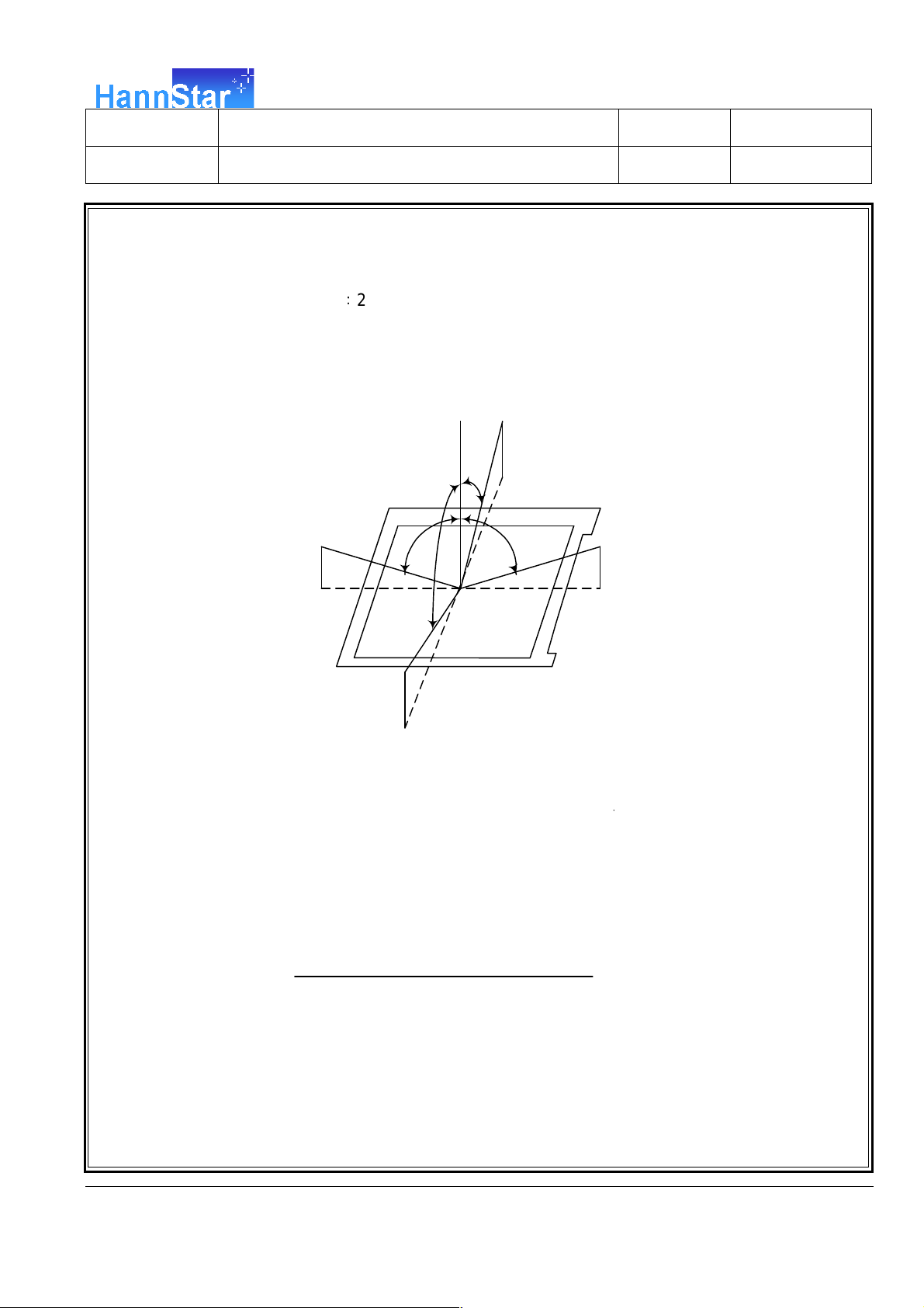
Note (1) Definition of Viewing Angle:
Θ
U
12’ o’clock
Φ=90
o
Φ=180
Θ
L
Θ
R
Φ=0o
Θ
D
6’ o’clock
Φ=270
o
Note (2) Definition of Contrast Ratio (CR) :
measured at the center point of panel
Luminance with all pixels white
CR =
Luminance with all pixels black
be disclosed, distributed or reproduced in whole or in part without written permission of HannStar Display
Corporation.
Page 8
HannStar Display Corp.
The information contained in this document is the exclusive property of HannStar Display Corporation. It shall not
Document Title HSD160PHW1 Specification for Wealth Star Page No. 8/26
Document No. DC130-004854 Revision 1.0
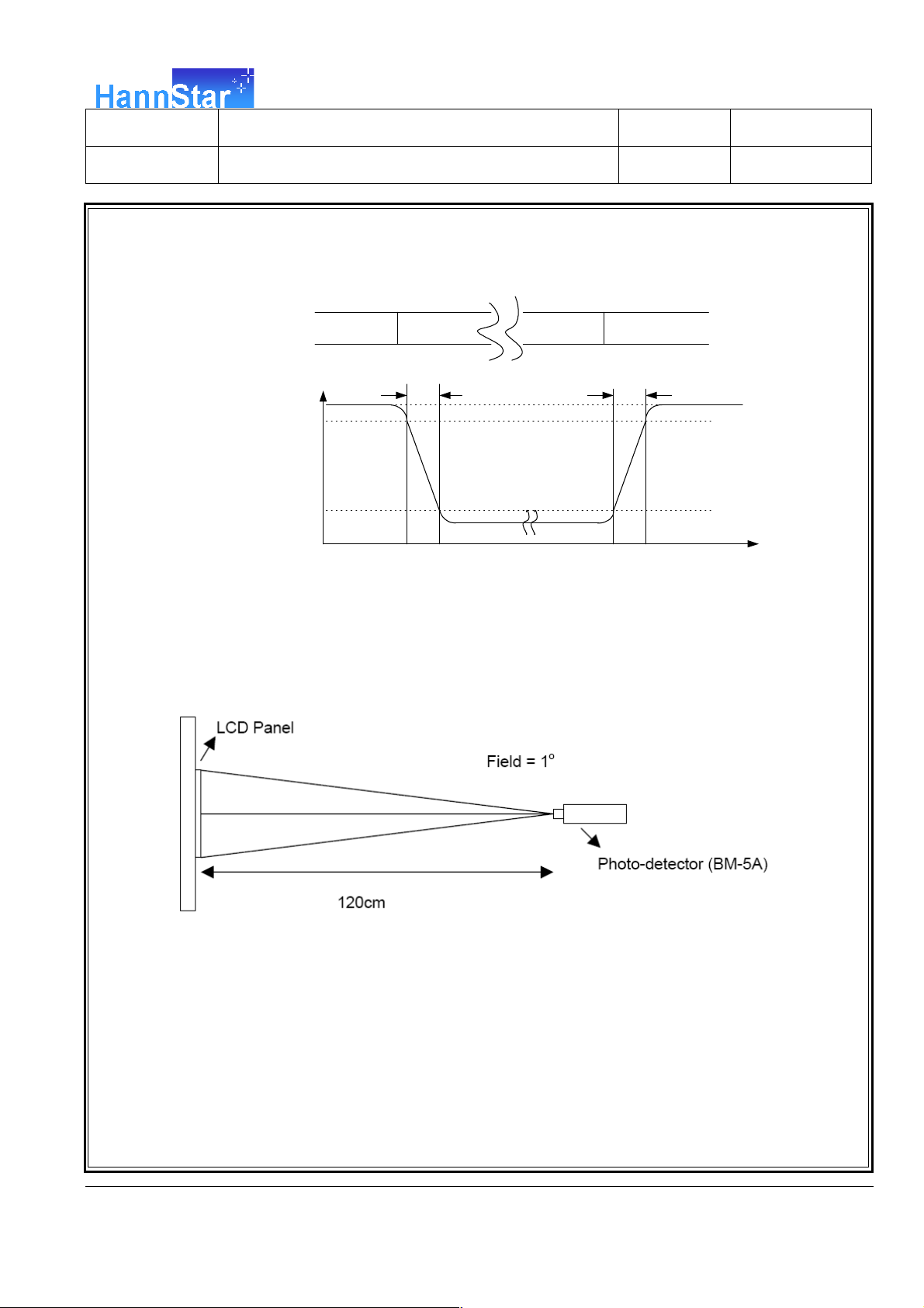
Note (3) Definition of Response Time : Sum of TR and TF
white(TFT OFF) black (TFT ON) white(TFT OFF)
100%
90%
T
R
T
F
Optical
response
10%
0%
time
Note (4) Definition of optical measurement setup
be disclosed, distributed or reproduced in whole or in part without written permission of HannStar Display
Corporation.
Page 9
HannStar Display Corp.
The information contained in this document is the exclusive property of HannStar Display Corporation. It shall not
Document Title HSD160PHW1 Specification for Wealth Star Page No. 9/26
Document No. DC130-004854 Revision 1.0
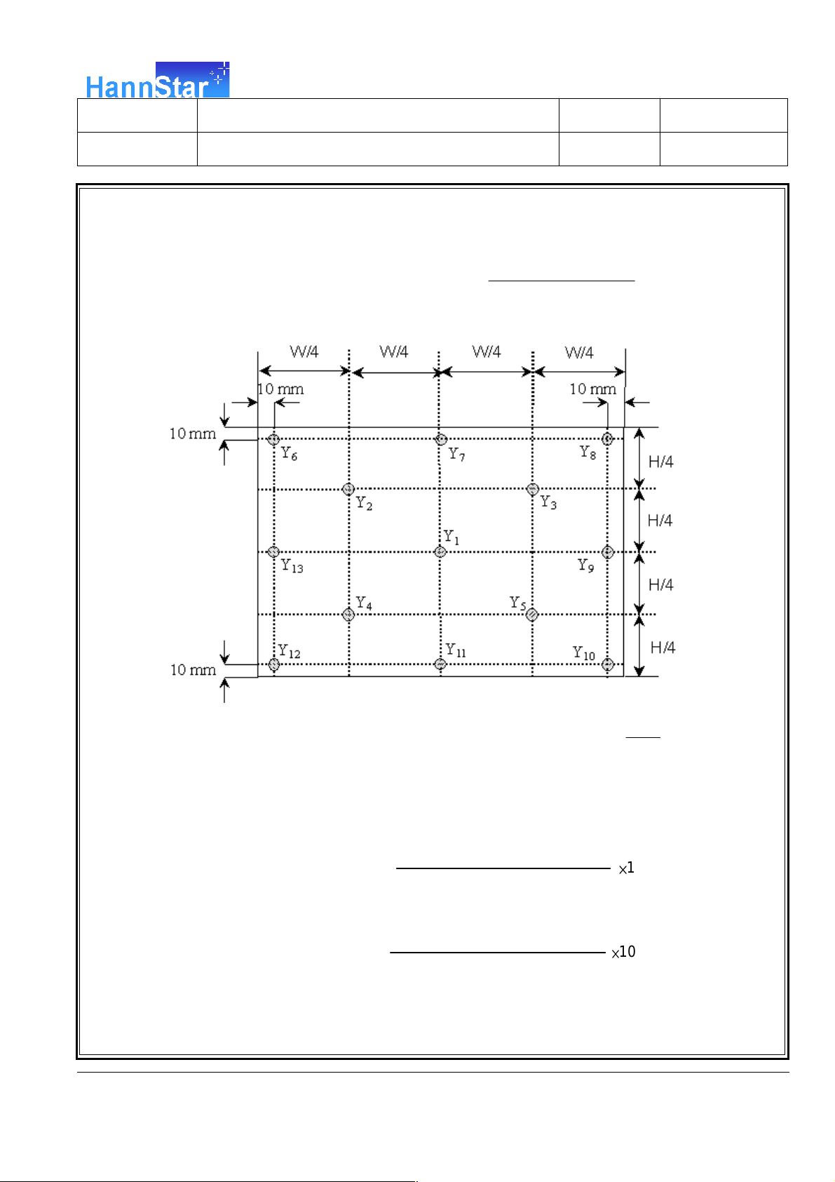
Note (5) Definition of Average Luminance Uniformity of White (5 Point)
Y1+Y2+Y3+Y4+Y5
Average Luminance Uniformity =
5
Note (6) Definition of brightness uniformity
Luminance uniformity(13points) = ×100%
be disclosed, distributed or reproduced in whole or in part without written permission of HannStar Display
Corporation.
Luminance uniformity(5 points) = ×100%
(Min Luminance of 5 points)
(Max Luminance of 5 points)
(Min Luminance of 13 points)
(Max Luminance of 13 points)
Page 10
HannStar Display Corp.
The information contained in this document is the exclusive property of HannStar Display Corporation. It shall not
1366 pixel (4098 Dots)
B G
LED
Document Title HSD160PHW1 Specification for Wealth Star Page No. 10/26
Document No. DC130-004854 Revision 1.0
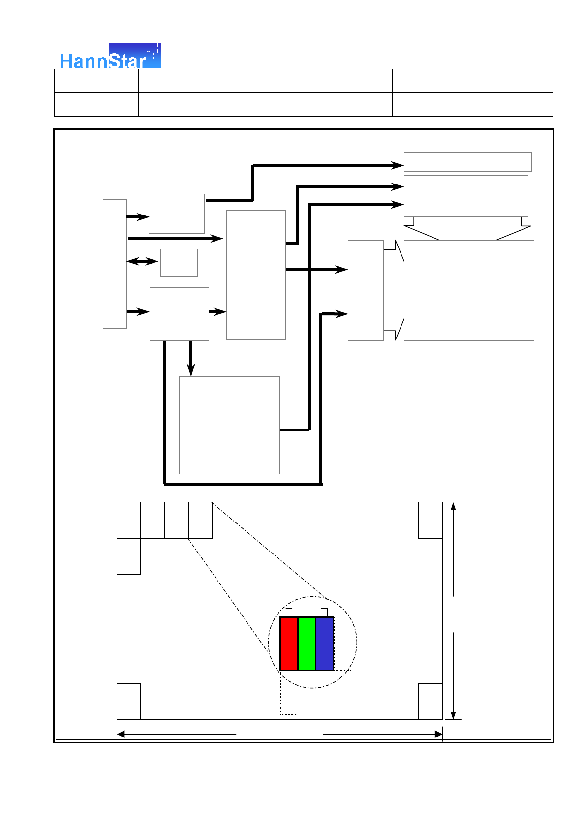
4.0 BLOCK DIAGRAM
4.1 TFT LCD Module:
X-driver IC
Driver
Timing
Connector
EDID
DC/DC
Converter
Controller
+
LVDS
Receiver
Liquid Crystal Panel
1366x768 pixels
Y-driver IC
4.2 Pixel Format
1,1
2,1
768,1
1,2 1,3 1,4
Gray scale
Manipulation
Voltage
Generation
Circuit
LCD Display Area
1 Pixel
R
R
R
1,1366
768,
1366
768 Lines
be disclosed, distributed or reproduced in whole or in part without written permission of HannStar Display
Corporation.
Page 11
HannStar Display Corp.
The information contained in this document is the exclusive property of HannStar Display Corporation. It shall not
scale of
Document Title HSD160PHW1 Specification for Wealth Star Page No. 11/26
Document No. DC130-004854 Revision 1.0
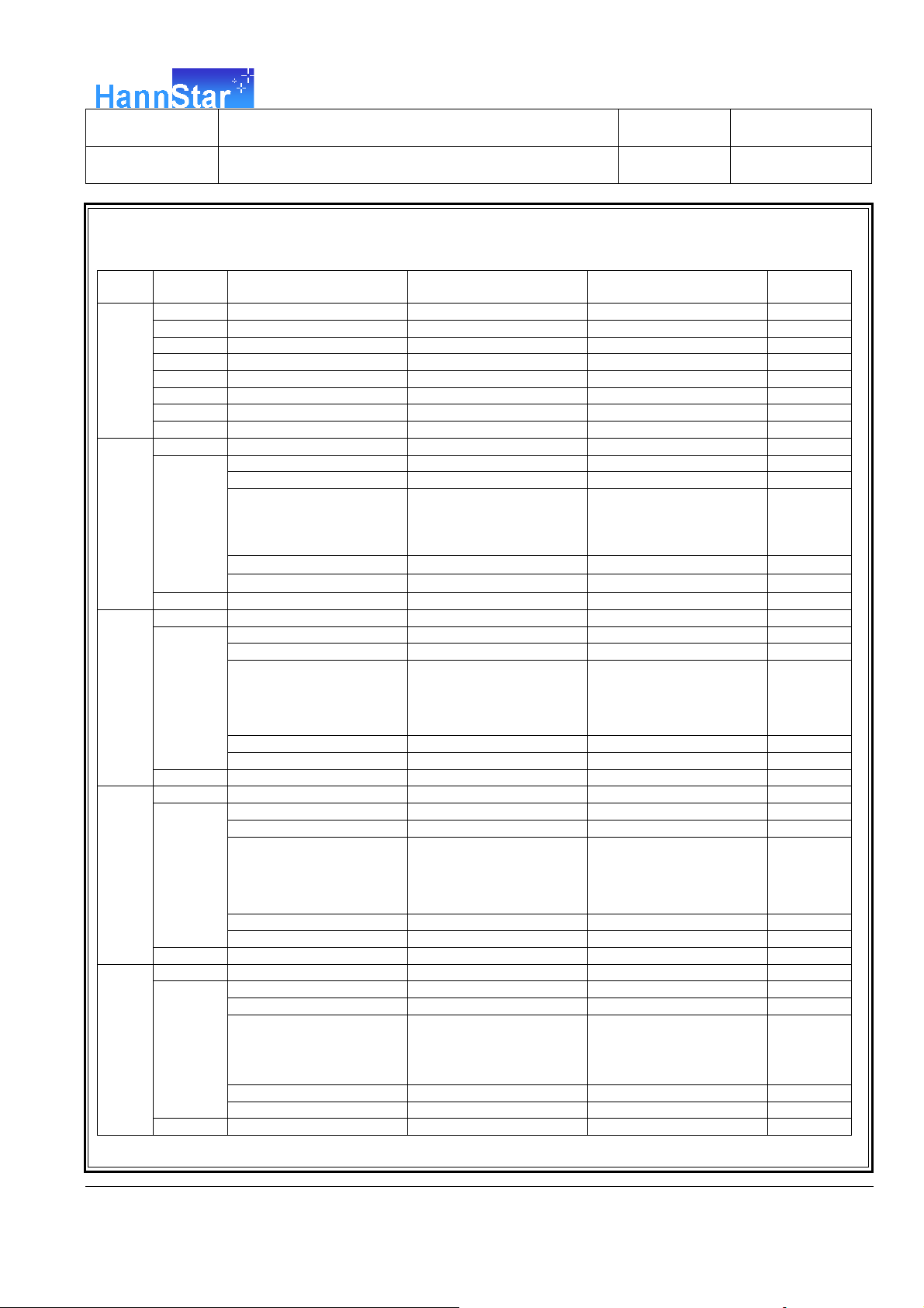
4.3 Relationship Between Displayed Color and Input
Basic
color
Gray
scale
of Red
Gray
scale of
Green
Gray
scale of
Blue
Gray
White &
Black
MSB LSB
Display
Black L L L L L L L L L L L L L L L L L L
Blue L L L L L L L L L L L L H H H H H H
Green L L L L L L H H H H H H L L L L L L
Light Blue L L L L L L H H H H H H H H H H H H
Red H H H H H H L L L L L L L L L L L L
Purple H H H H H H L L L L L L H H H H H H
Yellow H H H H H H H H H H H H L L L L L L
White H H H H H H H H H H H H H H H H H H
Black L L L L L L L L L L L L L L L L L L
Dark
Light
Red H H H H H H L L L L L L L L L L L L Red L63
Black L L L L L L L L L L L L L L L L L L
Dark
Light
Green L L L L L L H H H H H H L L L L L L Green L63
Black L L L L L L L L L L L L L L L L L L
Dark
Light
Blue L L L L L L L L L L L L H H H H H H Blue L63
Black L L L L L L L L L L L L L L L L L L
Dark
Light
White H H H H H H H H H H H H H H H H H H White L63
R5 R4 R3 R2 R1 R0
L L L L L H L L L L L L L L L L L L
L L L L H L L L L L L L L L L L L L
↑
↓
H H H H L H L L L L L L L L L L L L
H H H H H L L L L L L L L L L L L L
L L L L L L L L L L L H L L L L L L
L L L L L L L L L L H L L L L L L L
↑
↓
L L L L L L H H H H L H L L L L L L
L L L L L L H H H H H L L L L L L L
L L L L L L L L L L L L L L L L L H
L L L L L L L L L L L L L L L L H L
↑
↓
L L L L L L L L L L L L H H H H L H
L L L L L L L L L L L L H H H H H L
L L L L L H L L L L L H L L L L L H
L L L L H L L L L L H L L L L L H L
↑
↓
H H H H L H H H H H L H H H H H L H
H H H H H L H H H H H L H H H H H L
:
:
:
:
:
:
:
:
MSB LSB
G5 G 4 G3 G2 G1 G 0
:
:
:
:
:
:
:
:
MSB LSB
B5 B4 B3 B2 B1 B0
:
:
:
:
:
:
:
:
Gray scale
L3…L60
L3…L60
L3…L60
L3…L60
level
-
-
-
-
-
-
-
L0
L1
L2
L61
L62
L0
L1
L2
L61
L62
L0
L1
L2
L61
L62
L0
L1
L2
L61
L62
be disclosed, distributed or reproduced in whole or in part without written permission of HannStar Display
Corporation.
Page 12
HannStar Display Corp.
The information contained in this document is the exclusive property of HannStar Display Corporation. It shall not
Document Title HSD160PHW1 Specification for Wealth Star Page No. 12/26
Document No. DC130-004854 Revision 1.0
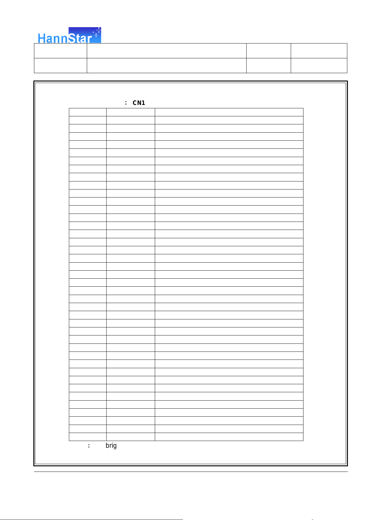
5.0 INTERFACE PIN CONNECTION
5.1
TFT LCD Module
Pin No. Signal Description
1 NC Not connection
2 AVDD Power Supply, 3.3V (typical)
3 AVDD Power Supply, 3.3V (typical)
4 DVDD DDC 3.3V power
5 NC No Connection
6 SCL EDID Clock
7 SDA EDID Data
8 Rin0- - LVDS differential data input (R0-R5,G0)
9 Rin0+ +LVDS differential data input (R0-R5,G0)
10 GND Ground
11 Rin1- - LVDS differential data input(G1-G5,B0-B1)
12 Rin1+ +LVDS differential data input (G1-G5,B0-B1)
13 GND Ground
14 Rin2- - LVDS differential data input (B2-B5,HS,VS,DE)
15 Rin2+ +LVDS differential data input (B2-B5,HS,VS,DE)
16 GND Ground
17 CIKIN- -LVDS differential clock input
18 CIKIN+ +LVDS differential clock input
19 GND Ground
20 NC No Connection
21 NC No Connection
22 GND Ground-Shield
23 NC No Connection
24 NC No Connection
25 GND Ground-Shield
26 NC No Connection
27 NC No Connection
28 GND Ground-Shield
29 NC No Connection
30 NC No Connection
31 VLED_GND LED Ground
32 VLED_GND LED Ground
33 VLED_GND LED Ground
34 NC No Connection
35 PWM PWM Signal for LED dimming control
36 LED_EN LED Enable Pin (+3V Input)
37 NC No Connection
38 VLED LED Power Supply 6-20V
39 VLED LED Power Supply 6-20V
40 VLED LED Power Supply 6-20V
Note
:
The brightness of LCD panel could be changed by adjusting PWM
:
::
:
CN1 (Input signal): IPEX 20455-040E-12 (IPEX or equivalent)
:
::
be disclosed, distributed or reproduced in whole or in part without written permission of HannStar Display
Corporation.
Page 13
HannStar Display Corp.
The information contained in this document is the exclusive property of HannStar Display Corporation. It shall not
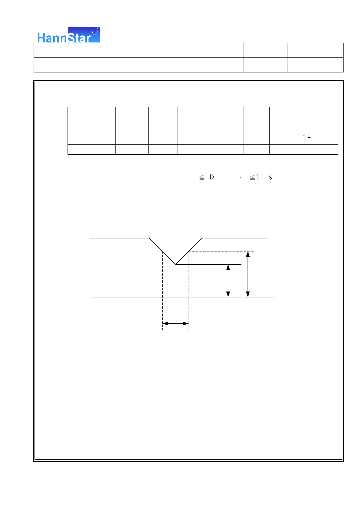
Supply Voltage
3.0v
td
Document Title HSD160PHW1 Specification for Wealth Star Page No. 13/26
Document No. DC130-004854 Revision 1.0
6.0 ELECTRICAL CHARACTERISTICS
6.1 TFT LCD Module
Item Symbol
VDD 3.0 3.3 3.6 V Note (1)
Current of
power supply
Inrush current
IDD - 0.3 - A VDD =3.3V、L0 pattern
I
RUSH
Note (1): V
dip condition:
DD-
When VDD operating within 2.7V≦VDD<3.0V,td≦10ms , the display may
momentarily become abnormal.
VDD<2.7V , VDD dip condition should also follow the Power On/Off
conditions for supply voltage.
.
Min. Typ. Max. Unit
Note
- - 1.50 A Note (2)
VDD
GND
be disclosed, distributed or reproduced in whole or in part without written permission of HannStar Display
Corporation.
Page 14
HannStar Display Corp.
The information contained in this document is the exclusive property of HannStar Display Corporation. It shall not
V
V
Document Title HSD160PHW1 Specification for Wealth Star Page No. 14/26
Document No. DC130-004854 Revision 1.0
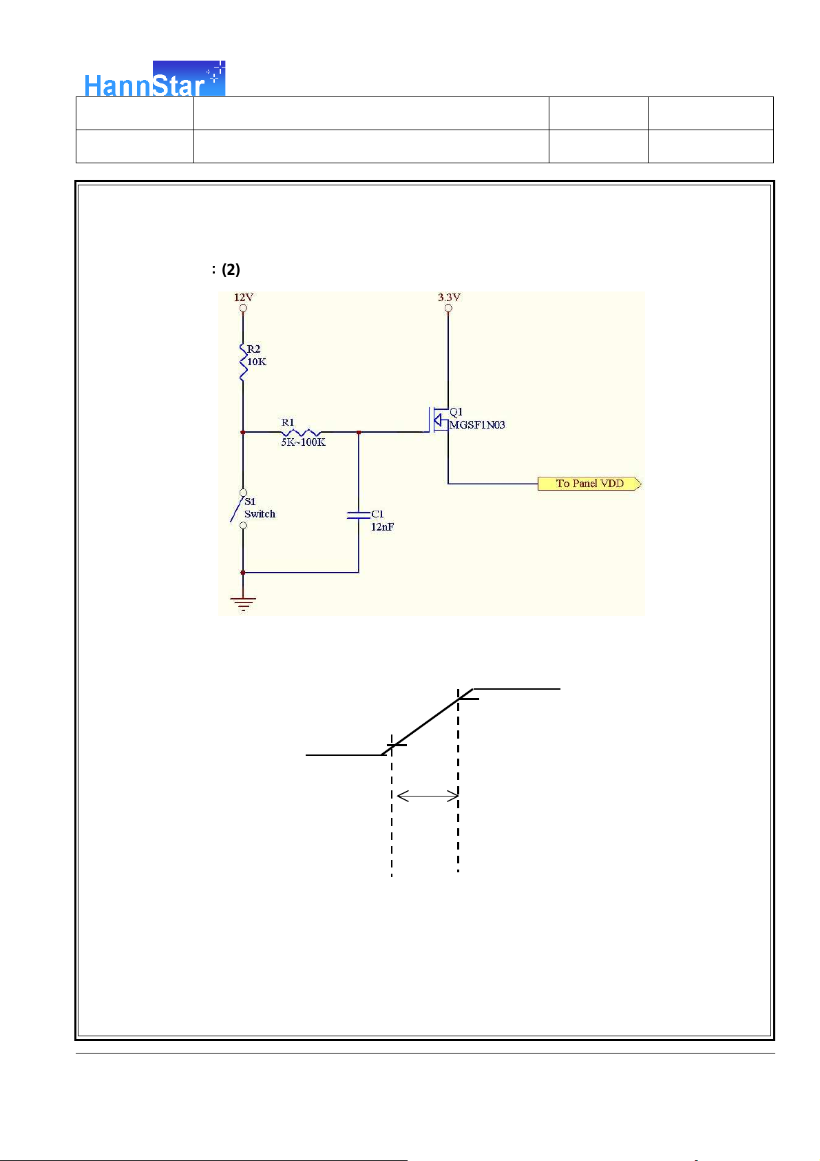
Note
:
(2) Power on Inrush current test circuit
:
::
0V
0.1VDD
rising time
in
0.9VDD
0.5 ms
DD
be disclosed, distributed or reproduced in whole or in part without written permission of HannStar Display
Corporation.
Page 15
HannStar Display Corp.
The information contained in this document is the exclusive property of HannStar Display Corporation. It shall not
2.5/7T
5.5/7T
Document Title HSD160PHW1 Specification for Wealth Star Page No. 15/26
Document No. DC130-004854 Revision 1.0
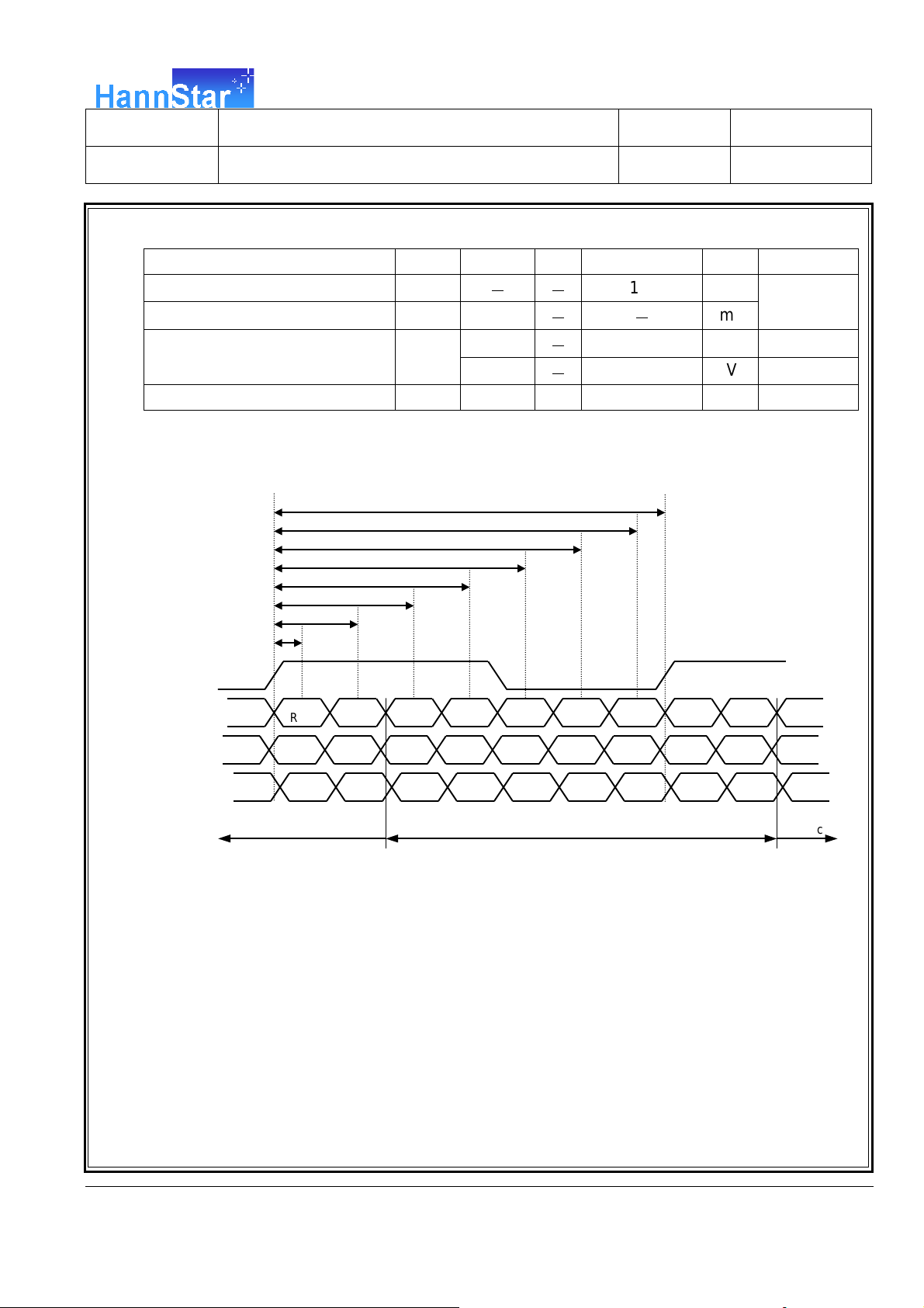
6.2 Switching Characteristics for LVDS Receiver
Item Symbol Min. Typ.
Max. Unit Conditions
Differential Input High Threshold Vth
Differential Input Low Threshold
Input Current
Differential input Voltage
Common Mode Voltage Offset VCM (|VID|/2)
6.3 Bit Mapping & Interface Definition
7T
6.5/7T
4.5/7T
3.5/7T
1.5/7T
0.5/7T
RCLK
Rin0
R[2]
R[1]
R[0]
Vtl -100
I
IN
|VID|
G[0]
R[5]
-
-10
0.1
R[4]
-
-
-
-
1.25
R[3]
100 mV
-
+10 uA
0.6 V
1.8-0.4-(|VID|/2) V
R[2]
R[1]
mV
R[0]
VCM=1.2V
G[0]
Rin1
G[3]
G[2]
G[1]
B[1]
B[0]
G[5]
G[4]
G[3]
G[2]
Rin2
B[4]
B[3]
B[2] DE
(VS)
(HS)
B[5]
B[4]
B[3]
Pervious cycle Current cycle
LVDS Receiver Input Timing Definition
for 6bits LVDS input
G[1]
B[2] DE
B[1]
Next cycle
be disclosed, distributed or reproduced in whole or in part without written permission of HannStar Display
Corporation.
Page 16
HannStar Display Corp.
The information contained in this document is the exclusive property of HannStar Display Corporation. It shall not
Document Title HSD160PHW1 Specification for Wealth Star Page No. 16/26
Document No. DC130-004854 Revision 1.0
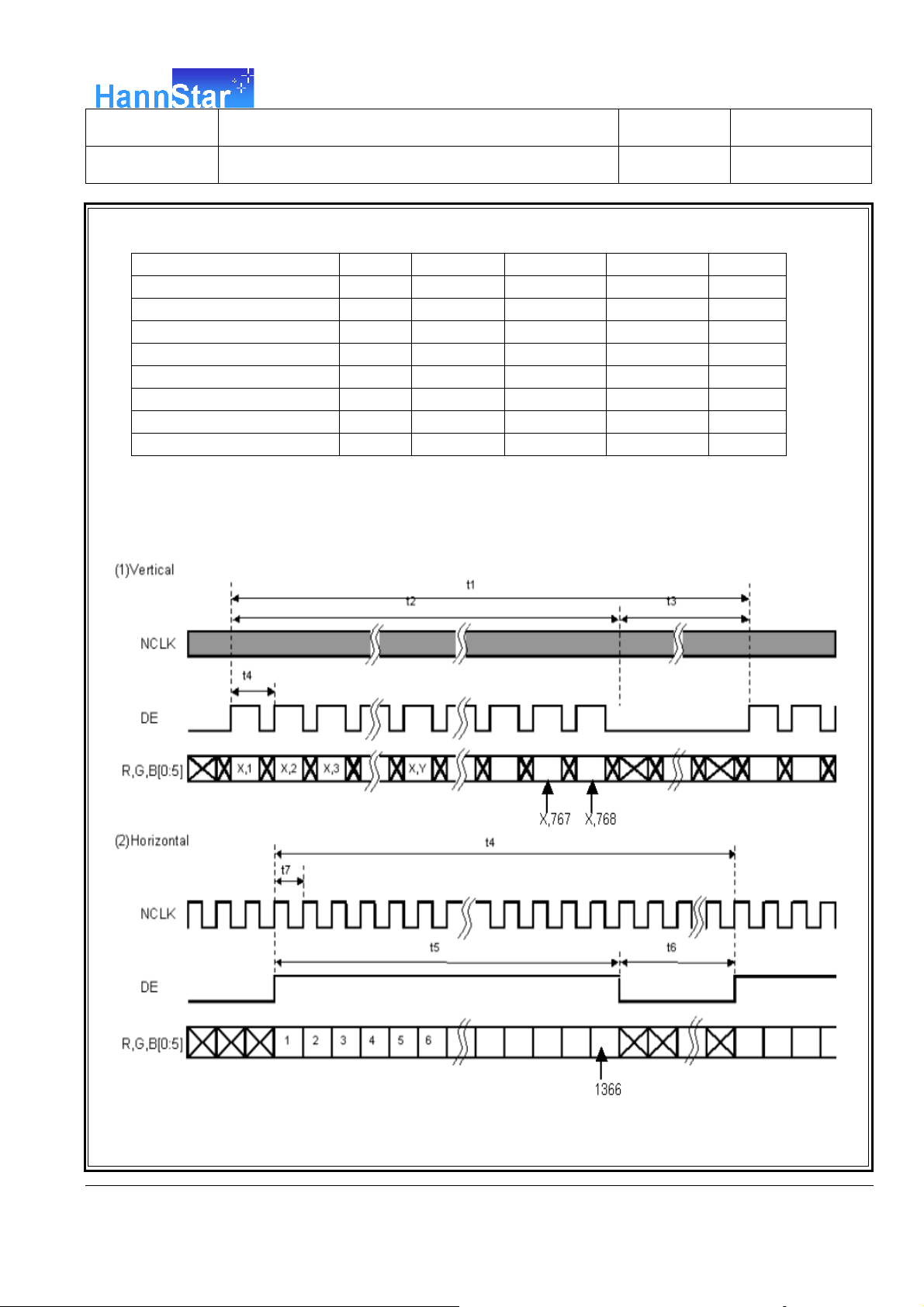
6.4 Interface Timing (DE mode)
Item Symbol
Frame Rate -- 55 60 - Hz
Frame Period t1 778 806 888 line
Vertical Display Time t2 768 768 768 line
Vertical Blanking Time t3 10 38 120 line
1 Line Scanning Time t4 1437 1560 1936 clock
Horizontal Display Time t5 1366 1366 1366 clock
Horizontal Blanking Time
t6 71 194 570 clock
Clock Rate t7 50.3 75.44 85 MHz
Timing Diagram of Interface Signal (DE mode)
Min. Typ. Max. Unit
be disclosed, distributed or reproduced in whole or in part without written permission of HannStar Display
Corporation.
Page 17
HannStar Display Corp.
The information contained in this document is the exclusive property of HannStar Display Corporation. It shall not
0.9V
DD
0.6V
0.6V
50%
Document Title HSD160PHW1 Specification for Wealth Star Page No. 17/26
Document No. DC130-004854 Revision 1.0
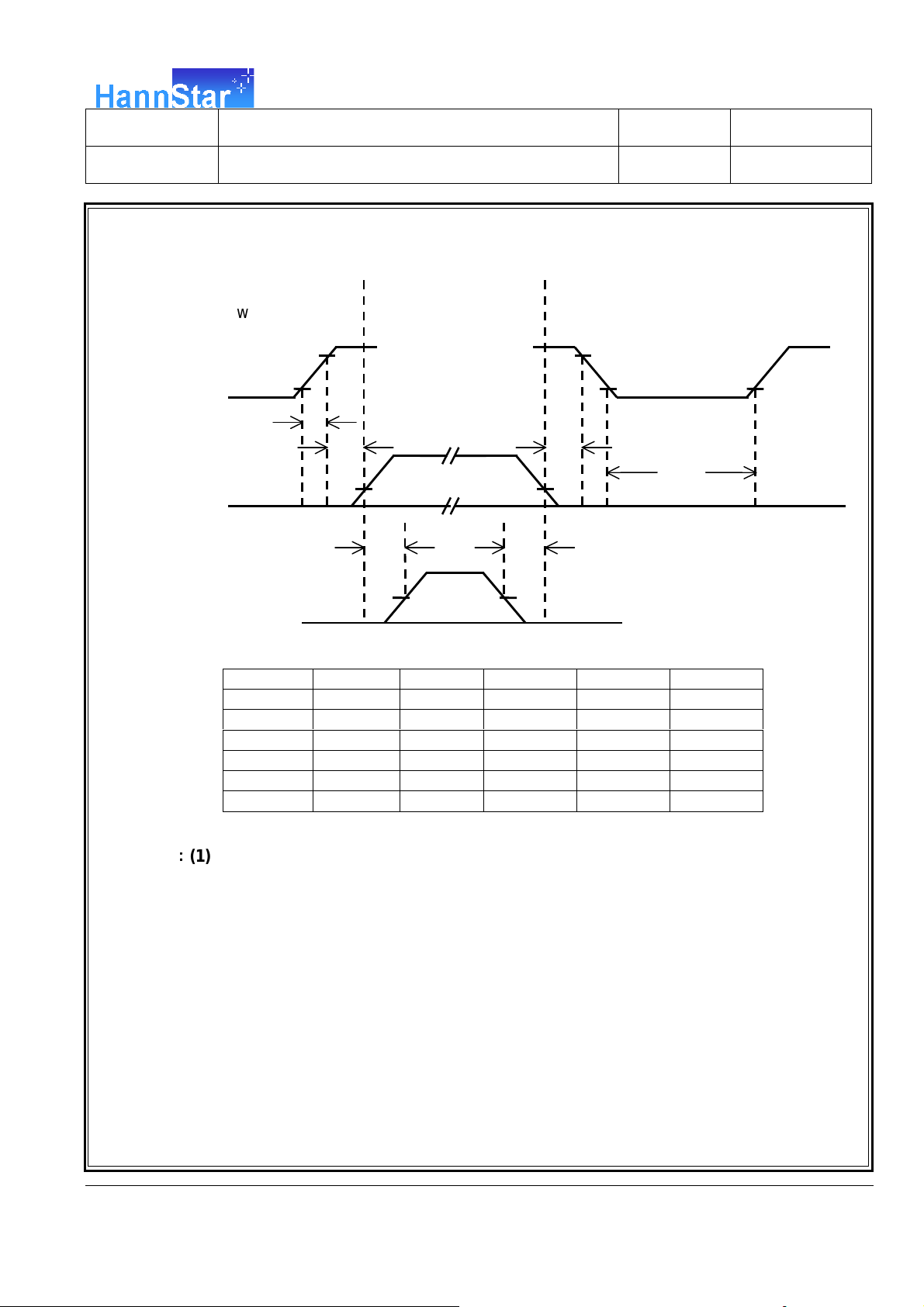
6.5 Power On / Off Sequence
Power On
Power
Off
Power Supply
0.9V
DD
0.1V
DD
0V
TP1
Signal
0V
Backlight
(Recommended
TP2
)
TP5
0.1V
TP3
TP6
50%
DD
TP4
0.1V
DD
Item Min. Typ. Max. Unit Remark
TP1 0.5 -- 10 msec
TP2 0.01 -- 50 msec
TP3 0 -- 50 msec
TP4 500 -- -- msec
TP5 200 -- -- msec
TP6 200 -- -- msec
Note
:
(1) The supply voltage of the external system for the module input should be the same
:
::
as the definition of VDD.
(2) Apply the lamp volatge within the LCD operation range. When the back-light turns
on before the LCD operation or the LCD truns off before the back-light turns off, the
display may momentarily become white.
(3) In case of VDD = off level, please keep the level of input signal on the low or
keep a high impedance.
(4) TP4 should be measured after the module has been fully discharged between
power off and on period.
(5) Interface signal shall not be kept at high impedance when the power is on.
be disclosed, distributed or reproduced in whole or in part without written permission of HannStar Display
Corporation.
Page 18
HannStar Display Corp.
The information contained in this document is the exclusive property of HannStar Display Corporation. It shall not
Document Title HSD160PHW1 Specification for Wealth Star Page No. 18/26
Document No. DC130-004854 Revision 1.0
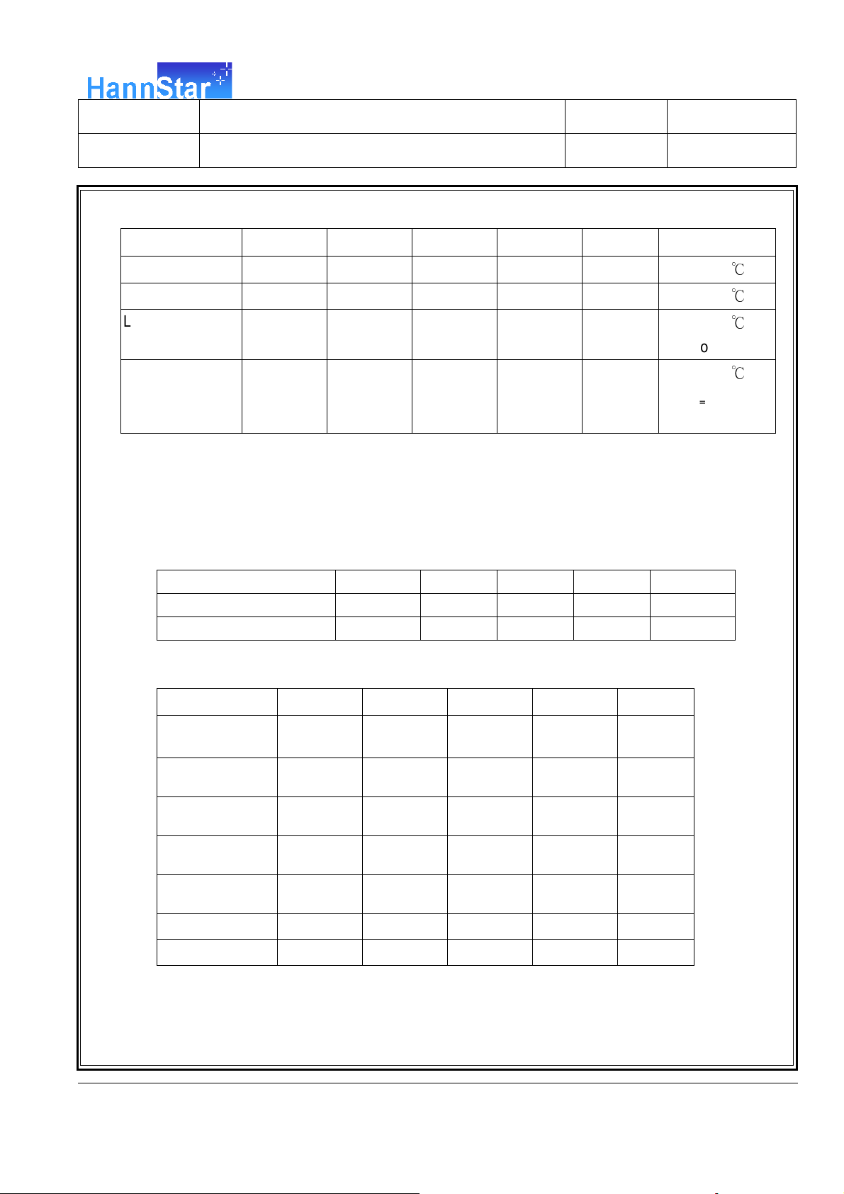
6.6 Backlight Unit
Parameter Symbol Min Typ Max Units Condition
LED Current IF -- 15 15.45 mA
LED Voltage VF 3.0 3.2 3.33 Volt
LED Power
P
--
LED
3.46 3.7
Watt
consumption
LED Life-Time N/A 12,000 -- -- Hour
Ta=25℃
Ta=25℃
Ta=25℃
Note (1)
Ta=25℃
IF=15mA
Note (2)
Note (1): Calculator value for reference P=IF x VF x N (LED Qty’)
Note (2): The LED lifetime defines as the estimated time to 50% degradation of final
luminous.
6.7 LED Driver
6.7.1 Absolute Maximum Ratings
Item Symbol Min. Max. Unit Note
LED Power Supply voltage
LED_EN, PWM pin Voltage
V
LED
VEN, V
-0.3 24 Volt
PWM
-- 5.5 Volt
6.7.2 DC Electrical Characteristics
Parameter Symbol Min Typ Max Units
LED Power
V
LED
6.0 -- 20.0 Volt
Supply Voltage
LED_EN High
Threshold
LED_EN Low
Threshold
PWM High
Threshold
PWM Low
Threshold
PWM Frequency
PWM Duty Cycle
be disclosed, distributed or reproduced in whole or in part without written permission of HannStar Display
Corporation.
V
V
V
PWMH
V
PWML
F
ENH
ENL
PWM
T
D
2.0 -- -- Volt
-- -- 0.3 Volt
3.0 -- -- Volt
-- -- 0.2 Volt
225
275
Hz
250
10 -- 100 %
Page 19
HannStar Display Corp.
The information contained in this document is the exclusive property of HannStar Display Corporation. It shall not
Dimming
Signal
, PWM
L
ED Enable
, LED_EN
0.9V
0.9V
T3
T
t
Document Title HSD160PHW1 Specification for Wealth Star Page No. 19/26
Document No. DC130-004854 Revision 1.0
Duty Cycle TD= (t / T) x 100%
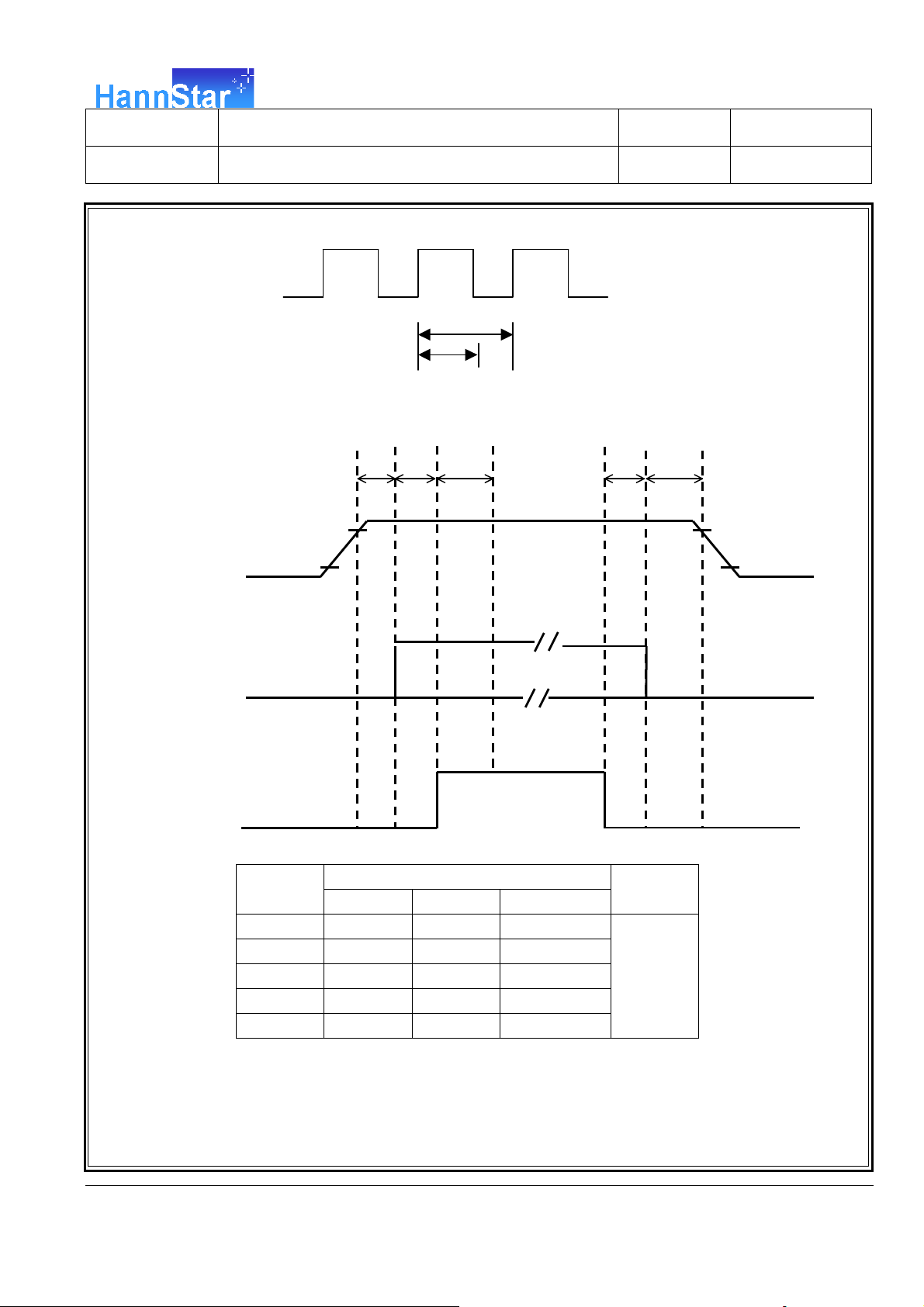
6.7.3 LED Power on/off sequence
LED Power Supply, V
LED
T1 T2 T4 T5
0.1V
0V
LED
0.1V
LED
0V
0V
Symbol
T1
T2
T3
T4
T5
Min Typ Max
10 -- -10 -- -50 -- --
0 -- --
10 -- --
Note (1): The duty of LED dimming signal should be more than 20% in T2 and T3
Note (2): PWM can adjust brightness to control Pin. Pulse duty the bigger the brighter.
Value
Unit
ms
be disclosed, distributed or reproduced in whole or in part without written permission of HannStar Display
Corporation.
Page 20
HannStar Display Corp.
The information contained in this document is the exclusive property of HannStar Display Corporation. It shall not
C(30min),100 cycles
100
20 40
50
Document Title HSD160PHW1 Specification for Wealth Star Page No. 20/26
Document No. DC130-004854 Revision 1.0
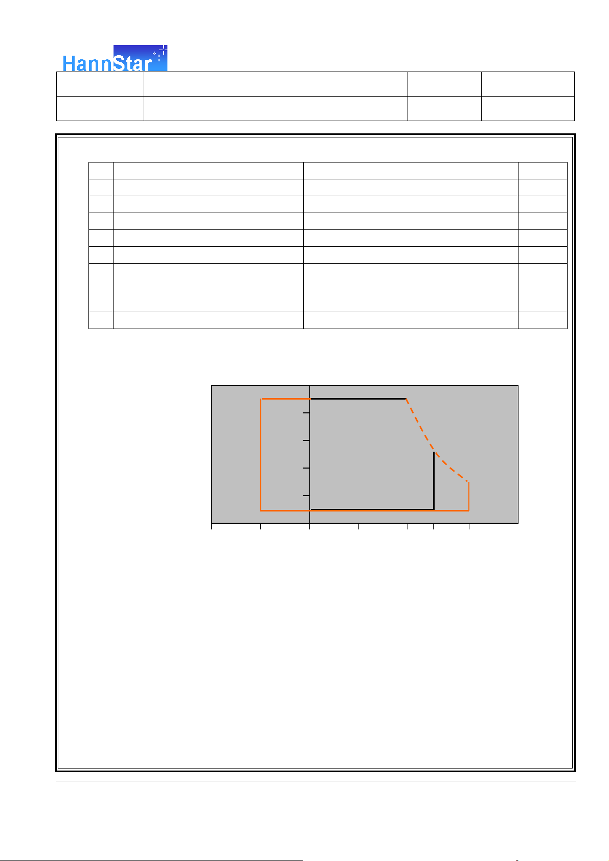
7.0 Reliability test items
No.
1 High Temperature Storage Ta=+60oC, 240hrs
2 Low Temperature Storage Ta=-20oC, 240hrs
High Temperature Operation Ta=+50oC, 500hrs
3
Low Temperature Operation Ta=0oC, 500hrs
4
5 Thermal Cycling Test (non operation) -20oC(30min)→+60
Vibration
6
7 Shock
Storage / Operating temperature
Note .Max wet bulb temp.=39oC
Item Conditions Remark
o
Sine Wave
1.5G, 5~500Hz, XYZ
30min/each direction
Half-Sine, 200G, 2ms, ±XYZ, 1time
-40
Humidity (%)
-20
90
80
60
40
Storage Range
20
10
0
0
Temperature (oC)
Operating Range
60
be disclosed, distributed or reproduced in whole or in part without written permission of HannStar Display
Corporation.
Page 21
HannStar Display Corp.
The information contained in this document is the exclusive property of HannStar Display Corporation. It shall not
Document Title HSD160PHW1 Specification for Wealth Star Page No. 21/26
Document No. DC130-004854 Revision 1.0
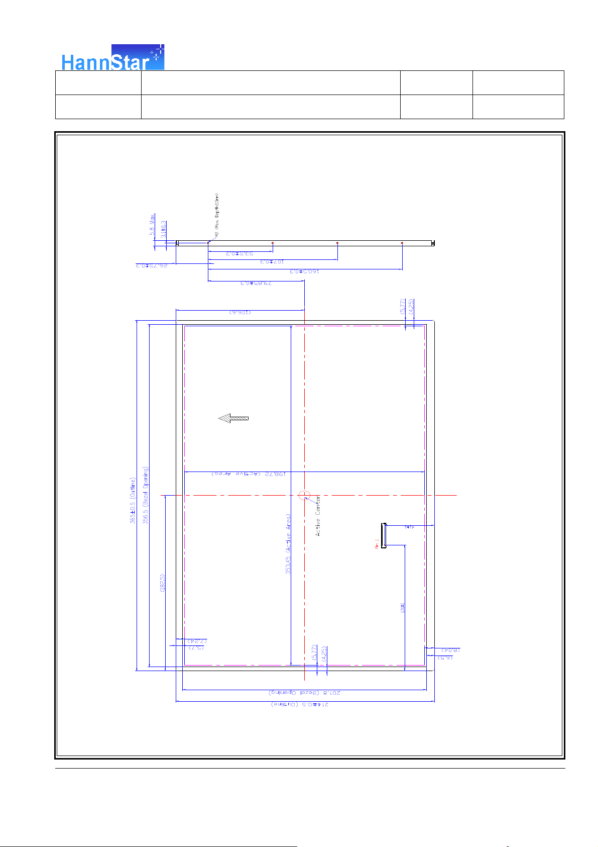
8.0 OUTLINE DIMENSION
8.1 Front View Outline Dimension
nit : mm
be disclosed, distributed or reproduced in whole or in part without written permission of HannStar Display
Corporation.
Page 22
HannStar Display Corp.
The information contained in this document is the exclusive property of HannStar Display Corporation. It shall not
Document Title HSD160PHW1 Specification for Wealth Star Page No. 22/26
Document No. DC130-004854 Revision 1.0
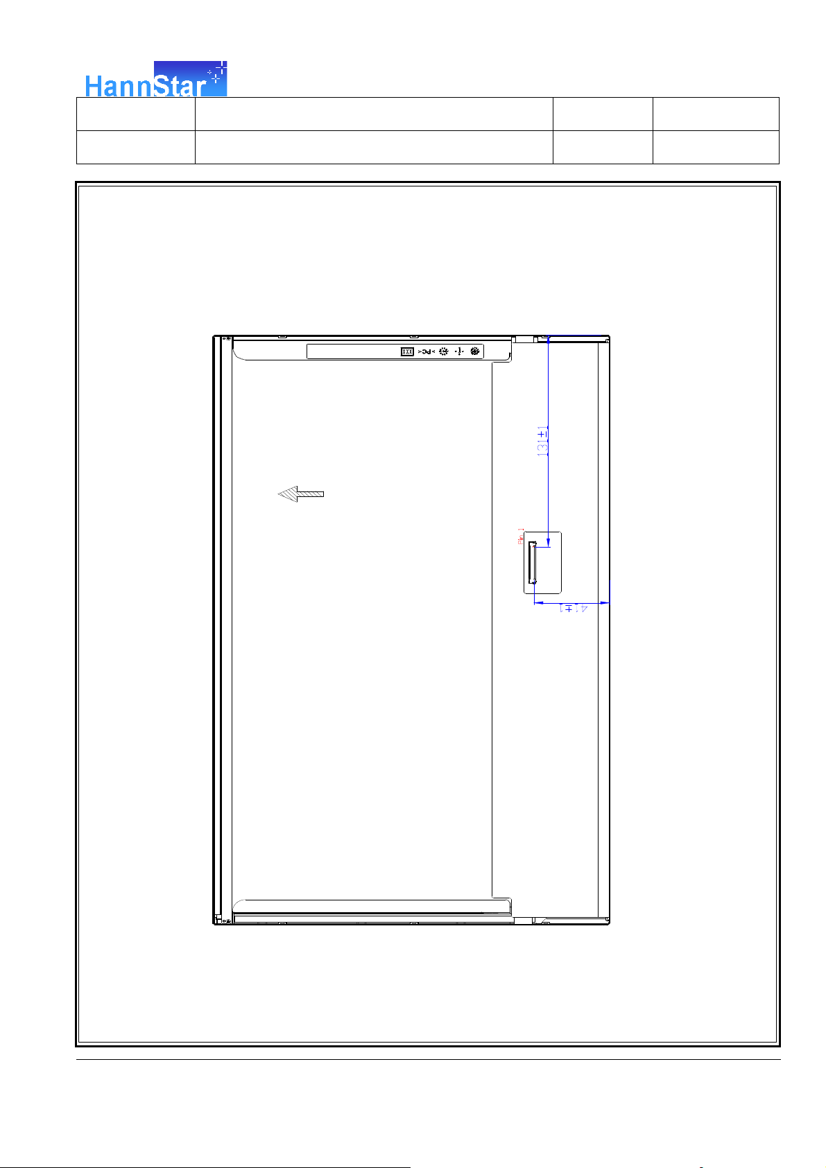
8.2 Back View Outline Dimension
be disclosed, distributed or reproduced in whole or in part without written permission of HannStar Display
Corporation.
Page 23
HannStar Display Corp.
The information contained in this document is the exclusive property of HannStar Display Corporation. It shall not
2
3
4
5
6
7
8
9
10
11
12
13
14
15
Document Title HSD160PHW1 Specification for Wealth Star Page No. 23/26
Document No. DC130-004854 Revision 1.0
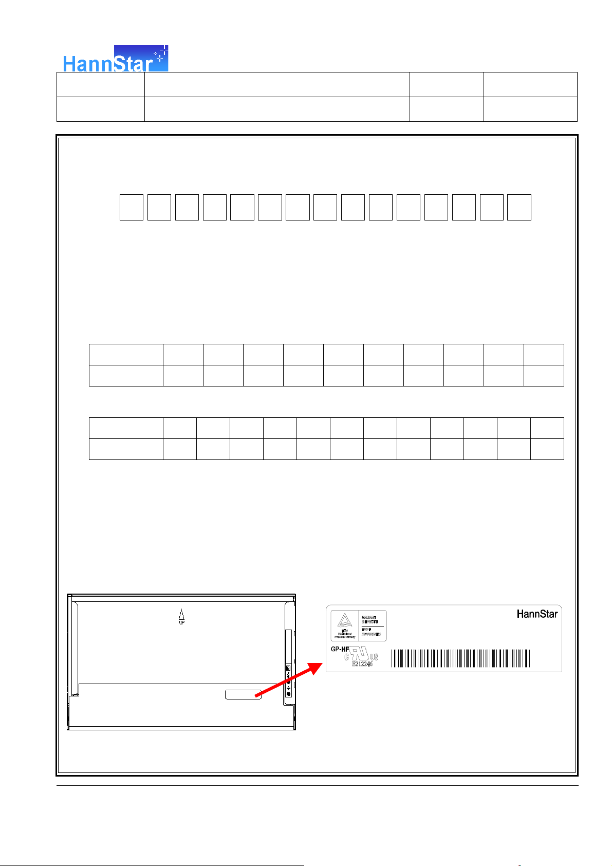
9.0 LOT MARK
9.1 Lot Mark
1
Code 1,2,3,4,5,6: HannStar internal flow control code.
Code 7: production location.
Code 8: production year.
Code 9: production month.
Code 10,11,12,13,14,15: serial number.
Note (1) Production Year
Year 2001 2002 2003 2004 2005 2006 2007 2008 2009 2010
Mark 1 2 3 4 5 6 7 8 9 0
Note (2) Production Month
Month Jan. Feb. Mar. Apr. May. Jun. Jul. Aug. Sep. Oct Nov. Dec.
Mark 1 2 3 4 5 6 7 8 9 A B C
9.2 Location of Lot Mark
(1) The label is attached to the backside of the LCD module.
(2) This is subject to change without prior notice.
HSD160PHW1
Rev: * -B EDX.X 6 A0
be disclosed, distributed or reproduced in whole or in part without written permission of HannStar Display
Corporation.
Page 24
HannStar Display Corp.
The information contained in this document is the exclusive property of HannStar Display Corporation. It shall not
Document Title HSD160PHW1 Specification for Wealth Star Page No. 24/26
Document No. DC130-004854 Revision 1.0
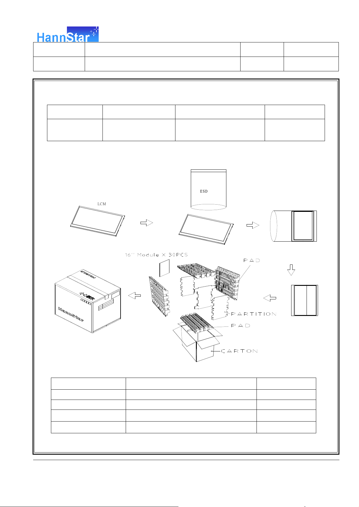
10.0 PACKAGE SPECIFICATION
10.1 Packing form
LCM Model LCM Qty. in the box
HSD160PHW-B
30 pcs/box
10.2 Packing assembly drawings
LCM
Inner Box Size
(mm)
530 x 314 x 464
ESD Bag
H
Notice
HSD160PHW1-B Material Notice
Box Corrugated Paper Board
Partition/Pad Corrugated Paper Board
Corner Pad Corrugated Paper Board
(AB Flute)
(B Flute)
(AB Flute)
ESD bag PE --
be disclosed, distributed or reproduced in whole or in part without written permission of HannStar Display
Corporation.
Page 25
HannStar Display Corp.
The information contained in this document is the exclusive property of HannStar Display Corporation. It shall not
Document Title HSD160PHW1 Specification for Wealth Star Page No. 25/26
Document No. DC130-004854 Revision 1.0
11.0 GENERAL PRECAUTION
11.1 Use Restriction
This product is not authorized for use in life supporting systems, aircraft navigation control
systems, military systems and any other application where performance failure could be
life-threatening or otherwise catastrophic.
11.2 Disassembling or Modification
Do not disassemble or modify the module. It may damage sensitive parts inside LCD
module, and may cause scratches or dust on the display. HannStar does not warrant the
module, if customers disassemble or modify the module.
11.3 Breakage of LCD Panel
11.3.1.If LCD panel is broken and liquid crystal spills out, do not ingest or inhale liquid
crystal, and do not contact liquid crystal with skin.
11.3.2. If liquid crystal contacts mouth or eyes, rinse out with water immediately.
11.3.3. If liquid crystal contacts skin or cloths, wash it off immediately with alcohol and
rinse thoroughly with water.
11.3.4. Handle carefully with chips of glass that may cause injury, when the glass is
broken.
11.4 Electric Shock
11.4.1. Disconnect power supply before handling LCD module.
11.4.2. Do not pull or fold the LED cable.
11.4.3. Do not touch the parts inside LCD modules and the fluorescent LED’s connector
or cables in order to prevent electric shock.
11.5 Absolute Maximum Ratings and Power Protection Circuit
11.5.1. Do not exceed the absolute maximum rating values, such as the supply voltage
variation, input voltage variation, variation in parts’ parameters, environmental
temperature, etc., otherwise LCD module may be damaged.
11.5.2. Please do not leave LCD module in the environment of high humidity and high
temperature for a long time.
11.5.3. It’s recommended to employ protection circuit for power supply.
11.6 Operation
11.6.1 Do not touch, push or rub the polarizer with anything harder than HB pencil lead.
11.6.2 Use fingerstalls of soft gloves in order to keep clean display quality, when persons
handle the LCD module for incoming inspection or assembly.
11.6.3 When the surface is dusty, please wipe gently with absorbent cotton or other soft
material.
be disclosed, distributed or reproduced in whole or in part without written permission of HannStar Display
Corporation.
Page 26
HannStar Display Corp.
The information contained in this document is the exclusive property of HannStar Display Corporation. It shall not
Document Title HSD160PHW1 Specification for Wealth Star Page No. 26/26
Document No. DC130-004854 Revision 1.0
11.6.4 Wipe off saliva or water drops as soon as possible. If saliva or water drops
contact with polarizer for a long time, they may causes deformation or color
fading.
11.6.5 When cleaning the adhesives, please use absorbent cotton wetted with a little
petroleum benzine or other adequate solvent.
11.7 Mechanism
Please mount LCD module by using mounting holes arranged in four corners tightly.
11.8 Static Electricity
11.8.1 Protection film must remove very slowly from the surface of LCD module to
prevent from electrostatic occurrence.
11.8.2 Because LCD module use CMOS-IC on circuit board and TFT-LCD panel, it is
very weak to electrostatic discharge. Please be careful with electrostatic
discharge. Persons who handle the module should be grounded through
adequate methods.
11.9 Strong Light Exposure
The module shall not be exposed under strong light such as direct sunlight. Otherwise,
display characteristics may be changed.
11.10 Disposal
When disposing LCD module, obey the local environmental regulations.
be disclosed, distributed or reproduced in whole or in part without written permission of HannStar Display
Corporation.
 Loading...