

Page 1
HannStar Display Corp.
Document Title
Document No. Revision 1.0
HSD150SXA1-A Tent ative Specification
Page No. 1 / 30
To :
Date :
HannStar Product S p ecification
Tentative
Model : HSD150SXA1-A
Note : 1. The information contained herein is preliminary and may be changed without prior notices.
2. Please contact HannStar Display Corp. before designing your product based on this module
specification.
3. The information contained herein is presented merely to indicate the characteristics and performance
of our products. No responsibility is assumed by HannStar for any intellectual property claims or other
problems that
The information contained in this document is the exclusive property of HannStar Display Corporation. It shall not be
disclosed, distributed or reproduced in whole or in part without written permission of HannStar Display Corporation.
may result from application based on the module described herein.
Page 2
HannStar Display Corp.
Document Title
Document No. Revision 1.0
HSD150SXA1-A Tent ative Specification
Page No. 2 / 30
Record of Revisions
Rev. Updated No. Date Description of change
1.0 --- July.01, 2002 Tentative specification for HSD150SXA1-A was first issued.
The information contained in this document is the exclusive property of HannStar Display Corporation. It shall not be
disclosed, distributed or reproduced in whole or in part without written permission of HannStar Display Corporation.
Page 3
HannStar Display Corp.
Document Title
Document No. Revision 1.0
HSD150SXA1-A Tent ative Specification
Page No. 3 / 30
Contents
1.0 General descriptions ……………………………….… p.4
2.0 Absolute maximum ratings ………………………….. p.5
3.0 Optical characteristics ……………………………….. p.7
4.0 Block diagram ………………………………………… p.12
5.0 I/O Connection Pin assignment ……………………….. p.15
6.0 Electrical Characteristics………………………….…………. p.17
7.0 Outline dimension …………………………….……… p.26
8.0 Lot Mark ……………………………………………….. p.28
9.0 General precaution ………………………………….. p.29
The information contained in this document is the exclusive property of HannStar Display Corporation. It shall not be
disclosed, distributed or reproduced in whole or in part without written permission of HannStar Display Corporation.
Page 4
HannStar Display Corp.
Document Title
Document No. Revision 1.0
HSD150SXA1-A Tent ative Specification
Page No. 4 / 30
1.0 GENERAL DESCRIPTIONS
1.1 Introduction
HannStar Display model HSD150SXA1-A is a color active matrix thin film transistor
(TFT) liquid crystal display (LCD) that uses amorphous silicon TFT as a switching device.
This model is composed of a TFT LCD panel, the voltage reference, common voltage,
DC-DC converter, column, and row driver circuit. This TFT LCD has a 15-inch diagonally
measured active display area with XGA resolution (768 vertical by 1024 horizontal pixel
array).
1.2 Features
■ 15” XGA TFT LCD panel
■ 2 CCFLs Backlight system
■ RSDS, 1 pixel/clock
■ Supported XGA (V:768 lines, H:1024 pixels) resolution
■ Supported to 75Hz refresh rate
■ Without LCD Timing Controller
1.3 General information
Item Specification Unit
Outline dimension 326.0×249.0×10.2 (Max.) with 2 brackets mm
Display area 304.1(H) x 228.1(V) (15.0” diagonal) mm
Number of Pixel 1024(H) x 768(V) pixels
Pixel pitch 0.297(H) x 0.297(V) mm
Pixel arrangement RG B Vertical stripe
Display color 6-bits driver with RSDS I/F
Display mode Normally white
Surface treatment Antiglare, Hard-Coating (3H)
Weight 1000 (Max.) g
Back-light 2-CCFLs, Top & bottom edge side
Input signal Source and Gate Driver control signals
Power consumption 11 W (Typ.), with back light W
Optimum viewing
direction
6 o’clock
1.4 Applications
■ Desktop monitors
■ Display terminals for AV applications
■ Monitors for industrial applications
The information contained in this document is the exclusive property of HannStar Display Corporation. It shall not be
disclosed, distributed or reproduced in whole or in part without written permission of HannStar Display Corporation.
Page 5
HannStar Display Corp.
Document Title
Document No. Revision 1.0
HSD150SXA1-A Tent ative Specification
Page No. 5 / 30
1.5 Mechanical Information
Item Min. Typ. Max. Unit
Horizontal(H) -
326.0
-mm
Vertical(V) - 249.0 - mmModule Size
Depth(D) - 9.9 10.2 mm
Weight (without inverter) -
960
1000 g
Notes: HannStar added 2 brackets to extend to 326.0 horizontal outlines.
2.0 ABSOLUTE MAXIMUM RATINGS
2.1 Absolute Rat i ng of Environment
Item Symbol Min. Max. Unit Note
Storage temperat ure T
Operating temperature T
Vibration (non-operating) V
Shock (non-operating) S
Storage humidity H
Operating humidity H
Low pressure (operating) P
Low pressure (non-operating) P
STG
OPR
NOP
NOP
STG
OP
LOP
LNOP
-20 60
050oC
-- 1.5 G (1)
-- 70 G (2)
10 90 %RH (3)
10 80 %RH (3)
697 -- HPa (4)
116 -- HPa (5)
o
C
Note (1) 5-500Hz sine wave, X,Y,Z each directions, 30 min/cycle.
(2) 11ms, ±X, ±Y, ±Z direction, one time each. For this shock test,
it is necessary to fill the silicon rubber between the shock jig as buffer.
o
(3) Max wet bulb temp. =39
C
(4) 2 hrs. (10000 feet)
(5) 24hrs. (50000 feet)
The information contained in this document is the exclusive property of HannStar Display Corporation. It shall not be
disclosed, distributed or reproduced in whole or in part without written permission of HannStar Display Corporation.
Page 6
HannStar Display Corp.
Document Title
HSD150SXA1-A Tent ative Specification
Page No. 6 / 30
Document No. Revision 1.0
Humidity (%)
100
90
80
60
40
Storage Range
20
10
0
-20-40
Operating Range
0
Temperature (
20 40 60
o
C)
50
65
2.2 Electrical Absolute Rating:
2.2.1 TFT LCD Module:
Item Symbol Condition
Input Power Voltage 1
V
Logic Signal input voltage V
Input Power Voltage 2
V
DD1
SIG
DD2
Normal
Normal -0.3 V
Normal
Value Unit
min. max.
+3.0 +3.8
+0.3 V
DD1
+10.0 +14.0
V(DC)
V(DC)
2.2.2 Back Light Unit:
Item Symbol Min. Max. Unit Note
Lamp voltage V
Lamp current
Lamp frequency f
L
I
L
L
Note: (1) Permanent damage may occur to the LCD module if beyond this specification.
Functional operation should be restricted to the conditions described under
Normal Operating Conditions.
0 2000 V(rms) (1)
-
7.0 mA (1)
0 100 KHz (1)
The information contained in this document is the exclusive property of HannStar Display Corporation. It shall not be
disclosed, distributed or reproduced in whole or in part without written permission of HannStar Display Corporation.
Page 7
HannStar Display Corp.
mSy
n
t
N
t
g
f
m
y
y
y
y
y
k
Document Title
HSD150SXA1-A Tent ative Specification
Page No. 7 / 30
Document No. Revision 1.0
3.0 OPTICAL CHARACTERISTICS
3.1 Measuring Condition
■ Measuring surrounding: dark room
■ Lamp current I
■ V
=3.3V, fV=60Hz, f
DD1
■ Surrounding temperature: 25±2
: (6.0)±0.1mA, lamp freq. FL=50KHz
BL
=32.5MHz
DCLK
o
C. 30min. Warm-up time.
3.2 Measuring Equipment
■ LCD-7000 of Otsuka Electric Corp., which utilized MCPD-7000 for Chromaticity
and BM-5A for other optical characteristics.
■ Measuring spot size: 10~12mm
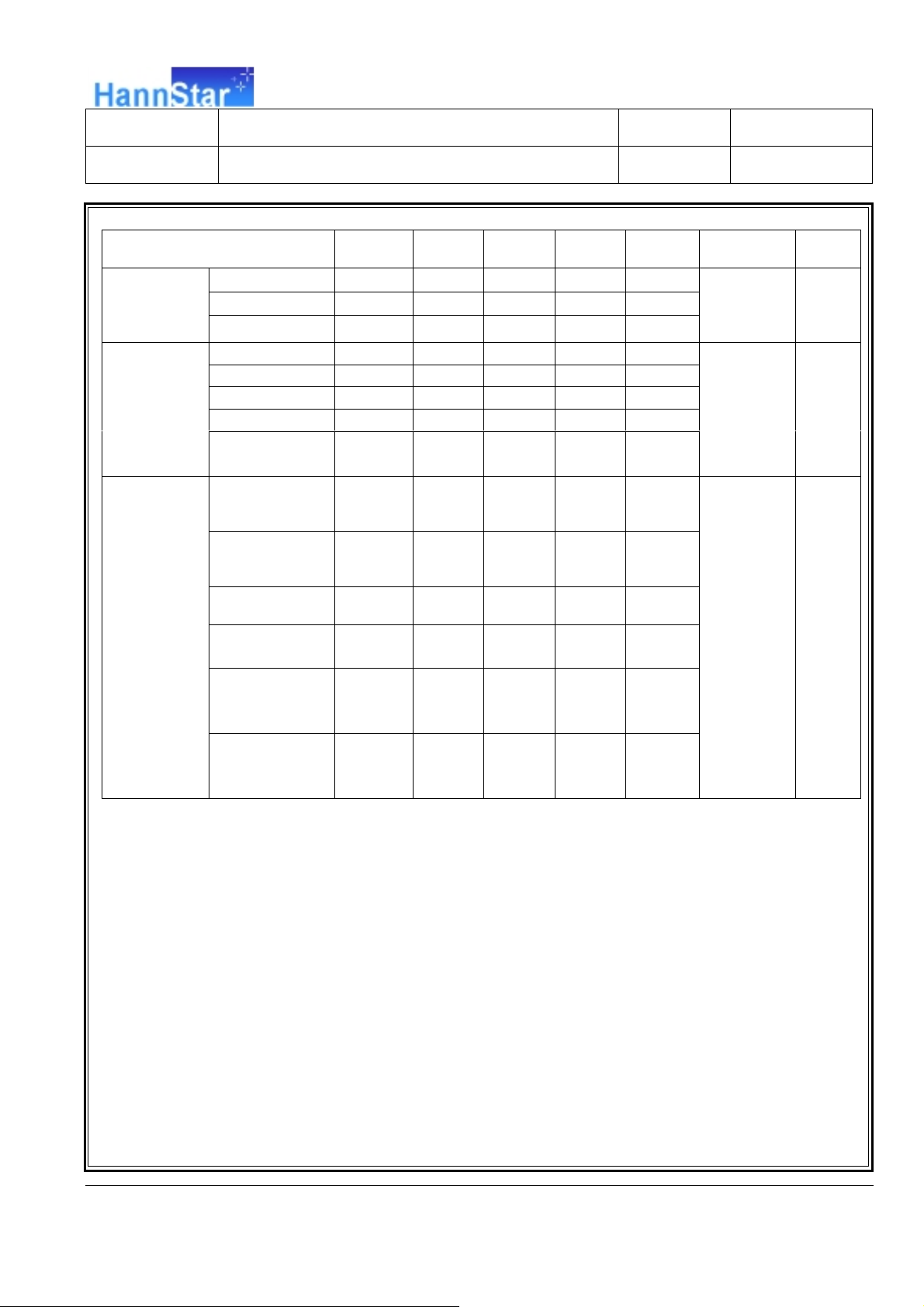
3.3 Optical specification
Ite
Contras
Response time
Rising T
Fallin
White luminance (center o
Red
Color
Green
chromaticity
(CIE1931)
Blue
White
Hor.
Viewing angle
Ve r.
Brightness uniformit
Gamma value -- -- -- % (6)
Cross tal
Image sticking 2hrs 5 sec (8)
Luminance uniformity
(TCO’99)
mbol Conditio
Min. Typ.Max.Uni
CR 300 400 -- (1)(2)
-- --
R
T
F
Y
L
Rx 0.597
R
Gx 0.266
G
Θ=0
o
φ=0
Normal
viewing
angle
o
0.308
0.566
Bx 0.119
B
0.086
Wx 0.285
W
Θ
L
Θ
R
Θ
H
Θ
L
B
UNI
CT(n) -- -- 1.2 (7)
L
R
CR>10
Θ=0
o
φ=0
0.303
75 80 -- % (5)
o
TR +TF
--
=(35)
--
msec (1)(3)
-- 250 -- cd/
0.627
0.338
0.296
0.596
0.149
0.116
0.315
0.333
0.657
0.368
0.326
0.626
0.179
0.146
0.345
0.363
-- 65 --
-- 65 --
-- 45 --
-- 55 --
1.7 (9)
2
ote
(1)
(1)(4)
The information contained in this document is the exclusive property of HannStar Display Corporation. It shall not be
disclosed, distributed or reproduced in whole or in part without written permission of HannStar Display Corporation.
Page 8
HannStar Display Corp.
Document Title
Document No. Revision 1.0
HSD150SXA1-A Tent ative Specification
Page No. 8 / 30
Note (1) Definition of Viewing Angle:
Φ
H
12’ o’clock
H
R
=90
o
=90
R
o
Θ
Θ
=90
L
Φ
Θ
L
o
Φ
L
Θ
6’ o’clock
=90
L
o
Φ
Note (2) Definition of Contrast Ratio(CR) :
measured at the center point of panel
Luminance with all pixels white (L63)
CR =
Luminance with all pixels black (L0)
The information contained in this document is the exclusive property of HannStar Display Corporation. It shall not be
disclosed, distributed or reproduced in whole or in part without written permission of HannStar Display Corporation.
Page 9
HannStar Display Corp.
Document Title
HSD150SXA1-A Tent ative Specification
Page No. 9 / 30
Document No. Revision 1.0
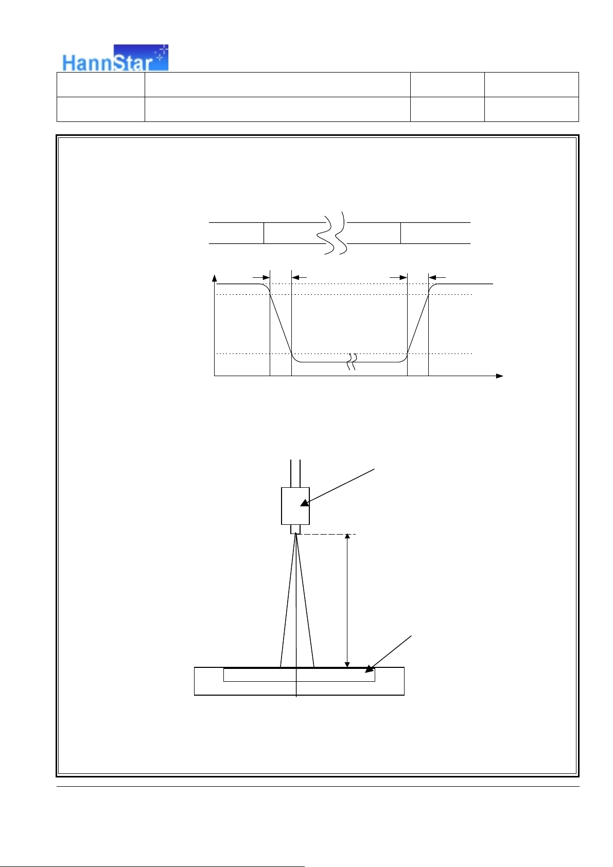
Note (3) Definition of Response Time: Sum of TR and T
white(TFT OFF) black (TFT ON) white(TFT OFF)
T
R
100%
90%
F
T
F
Optical
response
10%
0%
time
Note (4) Optical characteristic measurement setup
Field=2
o
50cm
Photo-detector (BM-5A)
LCD panel
The information contained in this document is the exclusive property of HannStar Display Corporation. It shall not be
disclosed, distributed or reproduced in whole or in part without written permission of HannStar Display Corporation.
Page 10

HannStar Display Corp.
Document Title
Document No. Revision 1.0
Note (5) Definition of brightness uniformity
Luminance uniformity =(Min Luminance)/(Max Luminance) x 100%
HSD150SXA1-A Tent ative Specification
10 mm
Page No. 10 / 30
10 mm
256 512 768
10 mm
192
384
576
10 mm
Note (6) Gamma values shall be measured at the center location.
nGs(S)
00 -
131 263 395 4 127 5 159 6 191 7 223 8 255 -
Relative Brightness (%) Remark
Min. Typical Max.
0.2
0.7
4.0
11.0
19.0
34.0
54.0
75.0
100.0
-
-
-
-
-
-
-
-
-
The information contained in this document is the exclusive property of HannStar Display Corporation. It shall not be
disclosed, distributed or reproduced in whole or in part without written permission of HannStar Display Corporation.
Page 11

HannStar Display Corp.
-
-
-
-
-
V
-
H
-
-
-
-
-
-
V
-
H
-
-
-
Document Title
HSD150SXA1-A Tent ative Specification
Page No. 11 / 30
Document No. Revision 1.0
Note (7) Definition of crosstalk CT (1) ~ CT (4)
L (n) – LB (n)
CT(n) = x 100% , n = 1 ~ 4
L (n)
2
Where L(n) = Luminance of point “n” at pattern A (cd/m
LB(n) = Luminance of point “n” at pattern B (cd/m
2
) , n=1~4
) , n=1~4
The location measured will be exactly the same in both patterns.
L0: Luminance with all pixels black
L63: Luminance with all pixels white
Gray scale: L31
1
1
4
V
8
V
L(1)
Gray scale: L0
1
1
V
8
V
4
L(4)
Gray scale: L31
LB(1)
LB(4)
L(3)
1
V
2
1
V
1
4
V
8
1
H
8
1
-
4
L(2)
1
8
1
H
1
H
2
H
4
-
1
V
2
1
-
V
1
4
8
H
LB(3)
V
1
H
8
1
-
4
LB(2)
1
8
1
H
1
H
2
H
4
H
Pattern A Pattern B
Note (8) Image sticking specifications as follows:
After 2 hours on condition of fixed patterns at 50℃ and 90%RH ,it does not remain in 5
seconds on the full white pattern.
Note (9)
TCO99 Certification Requirements and test methods for environmental labeling of Displays
[Flat] Report No.2 ( X1.5.2 Luminance Uniformity)
LR = ((L
max,+30deg
. / L
min,+30deg.
) + (L
max,-30deg
. / L
min,-30deg.
)) / 2
The information contained in this document is the exclusive property of HannStar Display Corporation. It shall not be
disclosed, distributed or reproduced in whole or in part without written permission of HannStar Display Corporation.
Page 12

HannStar Display Corp.
Document Title
Document No. Revision 1.0
HSD150SXA1-A Tent ative Specification
Page No. 12 / 30
4.0 BLOCK DIAGRAM
4.1 LCD Module Block Diagram:
X-Y FPC
(LCM Internal connector)
Interface
Connector
X-PCB
X-Y
Connector
50
CN1
1
DC-DC
Voltage
Reference
Circuit
Common
Voltage
Circuit
Drivers
RSDS
Source
Gate
Drivers
LCD Panel
768 lines x 1024 pixels
Y- P CB
The information contained in this document is the exclusive property of HannStar Display Corporation. It shall not be
disclosed, distributed or reproduced in whole or in part without written permission of HannStar Display Corporation.
Page 13

HannStar Display Corp.
Document Title
Document No. Revision 1.0
HSD150SXA1-A Tent ative Specification
Page No. 13 / 30
4.2 Pixel Format
1st Pixel 2nd Pixel 3rd Pixel 4t h Pixel 5th P ixel 6th Pixe l 1024t h Pixel
1st Line
2nd Line
3rd Line
4th Line
5th Line
6th Line
R G B R G B R G B R G B R G B R G B R G B
R G B R G B R G B R G B R G B R G B
R G B R G B R G B R G B R G B
R G B R G B R G B R G B
R G B R G B R G B
R G B R G B
R G B R G B R G B R G B R G B
R G B R G B R G B
R G B R G B R G B R G B
R G B
R G B R G B
LCD Display Area
1 Pixel =
R G B
768 Lines
768th Line
R G B R G B R G B R G B R G B R G B R G B
1024 Pixels
The information contained in this document is the exclusive property of HannStar Display Corporation. It shall not be
disclosed, distributed or reproduced in whole or in part without written permission of HannStar Display Corporation.
Page 14

HannStar Display Corp.
Document Title
HSD150SXA1-A Tent ative Specification
Page No. 14 / 30
Document No. Revision 1.0
4.3 Relationship between Displayed Color and Input Data
Basic
color
Gray
scale
of
Red
Gray
scale
of
Green
Gray
scale
of
Blue
Gray
scale
of
White
and
Black
Display
BlackLLLLLLLLLLLLLLLLLL -
Blue LLLLLLLLLLLLHHHHHH -
GreenLLLLLLHHHHHHL L LLLL -
Light BlueLLLLLLHHHHHHHHHHHH -
Red HHHHHHL L LLLLLLLLLL -
PurpleHHHHHHL LLLLLHHHHHH -
YellowHHHHHHHHHHHHL LLLLL -
WhiteHHHHHHHHHHHHHHHHHH BlackLLLLLLLLLLLLLLLLLL L0
Dark
Light
Red HHHHHHL L LLLLLLLLLLRed L63
BlackLLLLLLLLLLLLLLLLLL L0
Dark
Light
GreenLLLLLLHHHHHHL L LLLLGreen L63
BlackLLLLLLLLLLLLLLLLLL L0
Dark
Light
Blue LLLLLLLLLLLLHHHHHHBlue L63
BlackLLLLLLLLLLLLLLLLLL L0
Dark
Light
WhiteHHHHHHHHHHHHHHHHHHWhite L63
MSB LSB
R5 R4 R3 R2 R1 R0
LLLLLHLLLLLLLLLLLL L1
LLLLHLLLLLLLLLLLLL L2
↑
↓
HHHHLHLLLLLLLLLLLL L61
HHHHHLLLLLLLLLLLLL L62
LLLLLLLLLLLHLLLLLL L1
LLLLLLLLLLHLLLLLLL L2
↑
↓
LLLLLLHHHHLHLLLLLL L61
LLLLLLHHHHHLLLLLLL L62
LLLLLLLLLLLLLLLLLH L1
LLLLLLLLLLLLLLLLHL L2
↑
↓
LLLLLLLLLLLLHHHHLH L61
LLLLLLLLLLLLHHHHHL L62
LLLLLHLLLLLHLLLLLH L1
LLLLHLLLLLHLLLLLHL L2
↑
↓
HHHHLHHHHHLHHHHHLH L61
HHHHHLHHHHHLHHHHHL L62
:
:
:
:
:
:
:
:
MSB LSB
G5 G4 G3 G2G1 G0
:
:
:
:
:
:
:
:
MSB LSB
B5 B4 B3 B2 B1 B0
:
:
:
:
:
:
:
:
Gray scale
L3…L60
L3…L60
L3…L60
L3…L60
level
The information contained in this document is the exclusive property of HannStar Display Corporation. It shall not be
disclosed, distributed or reproduced in whole or in part without written permission of HannStar Display Corporation.
Page 15

HannStar Display Corp.
Document Title
HSD150SXA1-A Tent ative Specification
Page No. 15 / 30
Document No. Revision 1.0
5.0 I/O CONNECTION PIN ASSIGNMENT
5.1 Int erface FPC Connector CN1 (50-pins x 1) (HannStar Electrical Corp.)
I/F FRC Connector CN1
Pin No. Symbol Description
1 GND
2 D22P
3 D22N
4GND
5D21P
6D21N
7GND
8 D20P
9 D20N
10GND
11 D1 2P
12D12N
13GND
14D11P
15D11N
16GND
17D10P
18D10N
19GND
20 CLKP
21 CLKN
22 GND
23 D02P
24 D02N
25 GND
26 D01P
27 D01N
28 GND
29 D00P
30 D00N
31 GND
32 STH
33 LOAD
34 POL
35 REV
36 GND
37 CPV
38 STV
39 OE
40 NC
41 GND
42 VDD1
43 VDD1
44 VDD1
45 GND
46 VDD2
47 VDD2
48 ID1
49 ID2
50 ID3
Ground
RSDS Receiver Data + (Blue)
RSDS Receiver Data - (Blue)
Ground
RSDS Receiver Data + (Blue)
RSDS Receiver Data - (Blue)
Ground
RSDS Receiver Data + (Blue)
RSDS Receiver Data - (Blue)
Ground
RSDS Receiver Data + (Green)
RSDS Receiver Data - (Green)
Ground
RSDS Receiver Data + (Green)
RSDS Receiver Data - (Green)
Ground
RSDS Receiver Data + (Green)
RSDS Receiver Data - (Green)
Ground
RSDS Receiver clk +
RSDS Receiver clk Ground
RSDS Receiver Data + (Red)
RSDS Receiver Data - (Red)
Ground
RSDS Receiver Data + (Red)
RSDS Receiver Data - (Red)
Ground
RSDS Receiver Data + (Red)
RSDS Receiver Data - (Red)
Ground
Start pulse I/O
CK1
Odd & Even change
Data polarity inversion
Ground
Vertical shift clock input
Shift data I/O
Output enable pin
Ground
3.3V Power Input
3.3V Power Input
3.3V Power Input
Ground
12V Power Input
12V Power Input
Panel ID (Reserve pin)
Panel ID (Reserve pin)
Panel ID (Reserve pin)
The information contained in this document is the exclusive property of HannStar Display Corporation. It shall not be
disclosed, distributed or reproduced in whole or in part without written permission of HannStar Display Corporation.
Page 16

HannStar Display Corp.
Document Title
Document No. Revision 1.0
HSD150SXA1-A Tent ative Specification
Page No. 16 / 30
5.2 Back Light Unit (CCFL) Connectors:
CN2
CN3
CN2, 3: CCFL Power Source (BHR-03VS-1/Japan Solderless Terminal MFG Co., LTD)
Mating connector
Terminal No. Symbol Function
1 VL CCFL power supply (high voltage)
2NC
3GLCCFL power supply (low voltage)
Note 1) Please connects NC pin to nothing. Don’t connect it to ground nor to other signal
Input. (NC pin should be open.)
: SM02 (8.0)B-BHS-1/ Japan Solderless Terminal MFG Co., LTD
1)
No connection
The information contained in this document is the exclusive property of HannStar Display Corporation. It shall not be
disclosed, distributed or reproduced in whole or in part without written permission of HannStar Display Corporation.
Page 17

HannStar Display Corp.
Document Title
Document No. Revision 1.0
HSD150SXA1-A Tent ative Specification
Page No. 17 / 30
6.0 ELECTRICAL CHARACTERISTICS
6.1 Electrical System of LCD Module:
Value
Item Symbol Condition
Min. Typ. Max.
Input Voltage
Input
Rush Current
Input Signal
voltage
V
DD1
V
DD2
Irush
V
IH
V
IL
V
= +3.3V
DD1
V
= +12.0V.
DD2
High Level
Low Level
+3.0 +3.3 +3.6
+11.0 +12.0 +13.0
0.5
1.0
2.4 3.3 VDD1+0.2
0
-
0.9
Unit
V(DC)
A
V
V
6.2 Back-Light Unit:
The backlight system is an edge-lighting type with 2-CCFL (Cold Cathode Fluorescent Lamp).
The characteristics of four lamps are shown in the following tables.
Item Symbol Min. Typ. Max. Unit Note
Lamp current I
Lamp voltage V
Frequency f
L
L
L
Operating life time Hr 30,000
3.0 6.0 7.0 mA(rms) (1)
630 700 770 V(rms) IL=6.0 mA
50 55 80 KHz (2)
--
Hour (3)
1150 at 25oC
Startup voltage Vs
1350
--
V(rms)
at 0oC
The information contained in this document is the exclusive property of HannStar Display Corporation. It shall not be
disclosed, distributed or reproduced in whole or in part without written permission of HannStar Display Corporation.
Page 18

HannStar Display Corp.
Document Title
Document No. Revision 1.0
HSD150SXA1-A Tent ative Specification
Page No. 18 / 30
Note: (1) Lamp current is measured with current meter for high frequency as shown below. Specified
values are for a lamp.
1
2
3
A
INVERTER
LCD MODULE
1
2
3
A
(HIU-757)
(2) Lamp frequency may produce interference with horizontal synchronous frequency and this
may cause line flow on the display. Therefore lamp frequency shall be detached from the
horizontal synchronous frequency and its harmonics as far as possible in order to avoid
interference.
(3) Life time (Hr) can be defined as the time in which it continues to operate under the condition:
Temp. =25±3ºC, IL=6.0mA(rms.) and fL=50 KHz until one of the following event occurs:
1.When the brightness becomes 50%.
2.When the startup voltage (Vs) at 0ºC becomes higher than the maximal value of Vs
specified above.
The information contained in this document is the exclusive property of HannStar Display Corporation. It shall not be
disclosed, distributed or reproduced in whole or in part without written permission of HannStar Display Corporation.
Page 19

HannStar Display Corp.
Document Title
Document No. Revision 1.0
HSD150SXA1-A Tent ative Specification
Page No. 19 / 30
6.3 AC Electrical Characteristics:
6.3.1 AC Timing: (VDD1=3.0V~3.6V, T
OPR
=25 oC)
5)
Item Symbol Min. Typ. Max. Unit Signals Note
Reference
Signal
(Pixel Clock)
Reference
Signal
(DENB)
Vertical
Periodic
Horizontal
Periodic
Periodic
Line Periodic
Line Active
Line Blank
Frame Periodic
Frame Active
Frame Blank
Periodic
Pulse Width
Rising Time
Falling Time
Set-up Time
Hold Time
Period
Pulse Width
Rising Time
Falling Time
F1
T1=CLK
T2=T1*2
T3=Line 526 672 900 T2
T4 512512512T2
T5 14 160 388 T2
T6 773 806 950 Lines
T7 768 768 768 Lines
T8 5 --- --- Lines
T6 773 806 950 Lines
T9 11--- Lines
T11 --- 40 60 n-Sec
T12 --- 40 60 n-Sec
T13 700 800 --- n-Sec
T14 700 800 --- n-Sec
T15--- 1 --- Lines
T16A
T16B
T16C
T17A
T17B
T17C 2
T18A
T18B
T18C 2
50
12.5
25
1
1
264100
65
15.384
30.769
40
40
4
40
40
4
80
20
40
60
60 n-Sec
60
60 n-Sec
MHz
n-Sec
n-Sec
u-Sec
u-Sec
T2
STV
OE
CPV
LOAD
The information contained in this document is the exclusive property of HannStar Display Corporation. It shall not be
disclosed, distributed or reproduced in whole or in part without written permission of HannStar Display Corporation.
Page 20
HannStar Display Corp.
Document Title
Document No. Revision 1.0
HSD150SXA1-A Tent ative Specification
Page No. 20 / 30
Item Symbol Min. Typ. Max. Unit Signals Note
T19 15 --- --- n-Sec
T19A 6 --- --- n-Sec
T19B 6 --- --- n-Sec
T20 2 --- --- n-Sec
T21 1 --- --- n-Sec
T22 4 --- --- n-Sec
T23 2 --- --- n-Sec
T24 1CLKP --- 2CLKP n-Sec
T25 5CLKP ---
T26 5CLKP --- ---
T27 1CLKP --- ---
T28 4 --- --- n-Sec
2µs
CLKP
period
CLKP
period
CLKP
period
CLKP-
CLKN
STH
LOAD
Clock
Start pulse
Load
Pulse width
Pulse low period
Pulse high period
Data setup time
Data hold time
Setup time
Hold time
Signal pulse
width
Load high pulse
width
Load to STH
setup time
Last data time
Load(rising)~
Load(falling)
POL(rising) or
(falling) ~
T29 14 --- --- n-Sec
Load(rising)
Load(falling)~
POL(rising)or
T30 10 --- --- n-Sec
(falling)
Note 1) Refer to VESA standard.
Note 2) Please adjust LCD operating signal timing and FL driving frequency, to optimize the display
quality. There is a possibility that flicker is observed by the interference of LCD operating
signal timing and FL driving condition (especially driving frequency).
Note 3) All the timing setting should be confirmed with HannStar's FAE persons.
The information contained in this document is the exclusive property of HannStar Display Corporation. It shall not be
disclosed, distributed or reproduced in whole or in part without written permission of HannStar Display Corporation.
Page 21

HannStar Display Corp.
70%
30%
70%
30%
70%
30%
70%
30%
Document Title
HSD150SXA1-A Tent ative Specification
Page No. 21 / 30
Document No. Revision 1.0
6.3.2 AC Timing Charts:
(1). Reference Signal (pixel clock):
Reference Signal
T1
F1=1/T1
(Pixel Clock)
T2
Input Clock
The information contained in this document is the exclusive property of HannStar Display Corporation. It shall not be
disclosed, distributed or reproduced in whole or in part without written permission of HannStar Display Corporation.
Page 22

HannStar Display Corp.
30%
70%
50%
50%
30%
70%
70%
30%
70%
70%
Document Title
HSD150SXA1-A Tent ative Specification
Page No. 22 / 30
Document No. Revision 1.0
(2). Vertical Periodic (STV, OE, CPV):
T7 T8 T6
DENB
(For Reference)
STV
OE
CPV
LOAD
STH
DENB
(For Reference)
STV
OE
CPV
LOAD
T32
T16A
T3
T9
T13 T14
T16C
T4 T5
T12T11
T16B
T17C
T15
T17A
T17B T18B
T18A
T18C
The information contained in this document is the exclusive property of HannStar Display Corporation. It shall not be
disclosed, distributed or reproduced in whole or in part without written permission of HannStar Display Corporation.
Page 23

HannStar Display Corp.
Document Title
HSD150SXA1-A Tent ative Specification
Page No. 23 / 30
Document No. Revision 1.0
(3). Horizontal Periodic 1 (STH, CLK, DATA):
CLKP-CLKN
(RSDS)
STH
D00P-
D00N
D01P-
D01N
T
22
T
23
90% 90%
T
20
R(0)
R(2)
T
20
T
21
T
21
R(1)
R(3) R(3)
R(0)
R(2)
T
R(1)
19A
T
R(0)
R(2)
T
19B
19
R(1)
R(3)
R(2)
VIH
VCM
VIL
RSDS
RSDS
VIH
VCM
VIL
RSDS
RSDS
RSDS
RSDS
D02P-
D02N
D10P-
D10N
D11P-
D11N
D12P-
D12N
D20P-
D20N
D21P-
D21N
D22P-
D22N
R(4)
G(0)
G(2)
G(4)
B(0)
B(2)
B(4)
R(5) R(5)
G(1) G(1)
G(3) G(3)
G(5) G(5)
B(1) B(1)
B(3) B(3)
B(5) B(5)
R(4)
G(0)
G(2)
G(4)
B(0)
B(2)
B(4)
1st
Data
2nd
Data
R(4)
G(0)
G(2)
G(4)
B(0)
B(2)
B(4)
3rd
Data
R(5)
G(1)
G(3)
G(5)
B(1)
B(3)
B(5)
R(4)
G(0)
G(2)
G(4)
B(0)
B(2)
B(4)
The information contained in this document is the exclusive property of HannStar Display Corporation. It shall not be
disclosed, distributed or reproduced in whole or in part without written permission of HannStar Display Corporation.
Page 24

HannStar Display Corp.
Document Title
HSD150SXA1-A Tent ative Specification
Page No. 24 / 30
Document No. Revision 1.0
(4). Horizontal Periodic 2 (CLK, LOAD, STH, POL):
CLKP-CLKN
(RSDS)
STH
DxxP DxxN
(RSDS)
LOAD
POL
T
24
Invalid
EVEN EVEN EVEN
ODD
1st Data
ODD ODD
2nd Data
EVEN EVEN
ODD ODD
Last Data
T
27
T
26
10%
Invalid
T
28
T
90%
10%
25
90%
10%
T
29
90%
10%
T
30
90%
10%
InvalidInvalid
The information contained in this document is the exclusive property of HannStar Display Corporation. It shall not be
disclosed, distributed or reproduced in whole or in part without written permission of HannStar Display Corporation.
Page 25

HannStar Display Corp.
Document Title
Document No. Revision 1.0
6.4 Power On / Off Sequence:
HSD150SXA1-A Tent ative Specification
:
::
Page No. 25 / 30
Power On Power Off
TP1 TP2
Power supply
I
: 3.3V
DD1
Power supply
I
: 12.0V
DD2
Signal
0.9V
DD1
0.1V
DD2
TP3
TP5
DD2
0.6V
TP7
0.6V
TP8
0.9V
DD20.9V
TP4
0.1V
0.9V
DD2
DD1
TP9
Backlight
(Recommended)
50%
50%
Item Min. Typ. Max. Unit Remark
TP1 20 -- -- msec
TP2 20 -- -- msec
TP3 0 -- 10msec
TP4 0 -- 10msec
TP5 0 -- 50 msec
TP6 0 -- 50 msec
TP7 200 -- -- msec
TP8 200 -- -- msec
TP9 1 -- -- sec
Note:(1) The supply voltage of the external system for the module input should be the same as the
definition of VDD.
(2) Apply the lamp volatge within the LCD operation range. When the back-light turns on
before the LCD operation or the LCD truns off before the back-light turns off, the display
may momentarily become white.
(3) In case of V
= off level, please keep the level of input signal on the low or keep a high
DD
impedance.
(4) TP9 should be measured after the module has been fully discharged between power off
and on period.
(5)Interface signal shall not be kept at high impedance when the power is on.
The information contained in this document is the exclusive property of HannStar Display Corporation. It shall not be
disclosed, distributed or reproduced in whole or in part without written permission of HannStar Display Corporation.
Page 26

HannStar Display Corp.
Document Title
Document No. Revision 1.0
HSD150SXA1-A Tent ative Specification
Page No. 26 / 30
7.0 OUTLINE DIMENSION
7.1.1 Front View: Date: 20020315
The information contained in this document is the exclusive property of HannStar Display Corporation. It shall not be
disclosed, distributed or reproduced in whole or in part without written permission of HannStar Display Corporation.
Page 27
HannStar Display Corp.
Document Title
Document No. Revision 1.0
HSD150SXA1-A Tent ative Specification
Page No. 27 / 30
7.1.2 Back View: Date: 20020315
The information contained in this document is the exclusive property of HannStar Display Corporation. It shall not be
disclosed, distributed or reproduced in whole or in part without written permission of HannStar Display Corporation.
Page 28

HannStar Display Corp.
Document Title
Document No. Revision 1.0
HSD150SXA1-A Tent ative Specification
Page No. 28 / 30
8. LOT MARK
8.1 Lot Mark
123456789
code 1,2,3,4,5,6: HannStar internal flow control code.
code 7: production location.
code 8: production year.
code 9: production month.
code 10,11,12,13,14,15: serial number.
Note (1) Production Year
Year 1999 2000 2001 2002 2003 2004 2005 2006 2007 2008
Mark 9012345678
10 11 12 13 14 15
Note (2) Production Month
Month Jan. Feb. Mar. Apr. May. Jun. Jul. Aug. Sep. Oct Nov. Dec.
Mark 123456789ABC
8.2 Location of Lot Mark
(1) The label is attached to the backside of the LCD module.
(2) This is subject to change without prior notice.
HSD150SXA1
-A
Rev:
Lot mark
The information contained in this document is the exclusive property of HannStar Display Corporation. It shall not be
disclosed, distributed or reproduced in whole or in part without written permission of HannStar Display Corporation.
Page 29
HannStar Display Corp.
Document Title
Document No. Revision 1.0
HSD150SXA1-A Tent ative Specification
Page No. 29 / 30
9.0 GENERAL PRECAUTION
9.1 Use Restriction
This product is not authorized for use in life supporting systems, aircraft navigation control
systems, military systems and any other application where performance failure could be
life-threatening or otherwise catastrophic.
9.2 Disassembling or Modification
Do not disassemble or modify the module. It may damage sensitive parts inside LCD
module, and may cause scratches or dust on the display. HannStar does not warrant the
module, if customers disassemble or modify the module.
9.3 Breakage of LCD Panel
9.3.1 If LCD panel is broken and liquid crystal spills out, do not ingest or inhale liquid
crystal, and do not contact liquid crystal with skin.
9.3.2 If liquid crystal contacts mouth or eyes, rinse out with water immediately.
9.3.3 If liquid crystal contacts skin or cloths, wash it off immediately with alcohol and rinse
thoroughly with water.
9.3.4 Handle carefully with chips of glass that may cause injury, when the glass is broken.
9.4 Electric Shock
9.4.1 Disconnect power supply before handling LCD module.
9.4.2 Do not pull or fold the CCFL cable.
9.4.3 Do not touch the parts inside LCD modules and the fluorescent lamp’s connector
or cables in order to prevent electric shock.
9.5 Absolute Maximum Ratings and Power Protection Circuit
9.5.1 Do not exceed the absolute maximum rating values, such as the supply voltage
variation, input voltage variation, variation in parts’ parameters, environmental
temperature, etc., otherwise LCD module may be damaged.
9.5.2 Please do not leave LCD module in the environment of high humidity and high
temperature for a long time.
9.5.3 It’s recommended employing protection circuit for power supply.
9.6 Operation
9.6.1 Do not touch, push or rub the polarizer with anything harder than HB pencil lead.
9.6.2 Use fingerstalls of soft gloves in order to keep clean display quality, when persons
handle the LCD module for incoming inspection or assembly.
9.6.3 When the surface is dusty, please wipe gently with absorbent cotton or other soft
material.
9.6.4 Wipe off saliva or water drops as soon as possible. If saliva or water drops contact
with polarizer for a long time, they may causes deformation or color fading.
9.6.5 When cleaning the adhesives, please use absorbent cotton wetted with a little
petroleum benzine or other adequate solvent.
The information contained in this document is the exclusive property of HannStar Display Corporation. It shall not be
disclosed, distributed or reproduced in whole or in part without written permission of HannStar Display Corporation.
Page 30

HannStar Display Corp.
Document Title
Document No. Revision 1.0
HSD150SXA1-A Tent ative Specification
Page No. 30 / 30
9.7 Mechanism
Please mount LCD module by using mounting holes arranged in four corners tightly.
9.8 Static Electricity
9.8.1 Protection film must remove very slowly from the surface of LCD module to prevent
from electrostatic occurrence.
9.8.2 Because LCD module uses CMOS-IC on circuit board and TFT-LCD panel, it is v ery
weak to electrostatic discharge. Please be careful with electrostatic discharge.
9.8.3 Persons who handle the module should be grounded through adequate methods.
9.9 Strong Light Exposure
The module shall not be exposed under strong light such as direct sunlight. Otherwise,
display characteristics may be changed.
9.10 Disposal
When disposing LCD module, obey the local environmental regulations.
The information contained in this document is the exclusive property of HannStar Display Corporation. It shall not be
disclosed, distributed or reproduced in whole or in part without written permission of HannStar Display Corporation.
 Loading...