

Page 1
HannStar Display Corp.
Document Title HSD150SX87 Product Information Page No.
Document No. Revision 1.0
1 / 28
HannStar Product Information
Model :
HSD150SX87
- A
Note: 1. Please contact HannStar Display Corp. before designing your product based on this module
specification.
2. The information contained herein is presented merely to indicate the characteristics and perform ance
of our products. No responsibility is assumed by HannStar for any intellectual property claims or other
problems that
may result from application based on the module described herein.
The information contained in this document is the exclusive property of HannStar Display Corporation. It shall not be
disclosed, distributed or reproduced in whole or in part without written permission of HannStar Display Corporation.
Page 2
HannStar Display Corp.
Document Title HSD150SX87 Product Information Page No.
Document No. Revision 1.0
2 / 28
Record of Revisions
Rev. Updated No. Date Description of change
0.1 ─ Mar.03,2003 Tentative s
issued.
0.2 ─ Mar.18,2003 1. Modify the typical values of the viewing angle and the
brightness unifomity in the page 7.
2. Increase the in-rush current condition in the page 16.
3. Modify the AC timing specification in the page 19.
4. Increase the graphic of the initial condition of the AC
pecification for HSD150SX87-A was first
timing specification in the page 23.
0.3 ─ Mar.22,2003 1.modify page 19.
2.Modify viewing angle in page 7.
3.Add suggest timing in page 25
The information contained in this document is the exclusive property of HannStar Display Corporation. It shall not be
disclosed, distributed or reproduced in whole or in part without written permission of HannStar Display Corporation.
Page 3

HannStar Display Corp.
Document Title HSD150SX87 Product Information Page No.
Document No. Revision 1.0
3 / 28
Contents
1.0 General descriptions ……………………………….… p.4
2.0 Absolute maximum ratings ………………………….. p.5
3.0 Optical characteristics ……………………………….. p.7
4.0 Block diagram ………………………………………… p.11
5.0 I/O Connection Pin assignment ……………………….. p.14
6.0 Electrical Characteristics ………………….…………. p.16
7.0 Suggestion Timing …………………………….……… p.25
8.0 Outline dimension p 27
9.0 Lot Mark ……………………………………………….. p.28
10.0 Package Specification ……………………………...… P.30
11.0 General precaution ………………………………….. p.33
The information contained in this document is the exclusive property of HannStar Display Corporation. It shall not be
disclosed, distributed or reproduced in whole or in part without written permission of HannStar Display Corporation.
Page 4
HannStar Display Corp.
Document Title HSD150SX87 Product Information Page No.
Document No. Revision 1.0
4 / 28
1.0 GENERAL DESCRIPTIONS
1.1 Introduction
HannStar Display model HSD150SX87-A is a color active matrix thin film transistor
(TFT) liquid crystal display (LCD) that uses amorphous silicon TFT as a switching device.
This model is composed of a TFT LCD panel, the voltage reference, common voltage,
DC-DC converter, column, and row driver circuit. This TFT LCD has a 15-inch diagonally
measured active display area with XGA resolution (768 vertical by 1024 horizontal pixel
array).
1.2 Features
■ 15” XGA TFT LCD panel
■ 2 CCFLs Backlight system
■ Supported XGA (V:768 lines, H:1024 pixels) resolution
■ Supported to 75Hz refresh rate
■ Without LCD Timing Controller
1.3 General information
Item Specification Unit
Outline dimension 321.0× 249.0× 10.5 (typ.) Mm
Display area 304.1(H) x 228.1(V) (15.0” diagonal) Mm
Number of Pixel 1024(H) x 768(V) Pixels
Pixel pitch 0.297(H) x 0.297(V) Mm
Pixel arrangement RGB Vertical stripe
Display color 6-bits driver
Display mode Normally white
Surface treatment Antiglare, Hard-Coating(3H)
Weight 900(typ.) G
Back-light 2-CCFLs, Top & bottom edge side
Input signal Source and Gate Driver control signals
Power consumption 12 W(typ.), with back light W
Optimum viewing
direction
6 o’clock
1.4 Applications
■ Desktop monitors
■ Display terminals for AV applications
■ Monitors for industrial applications
The information contained in this document is the exclusive property of HannStar Display Corporation. It shall not be
disclosed, distributed or reproduced in whole or in part without written permission of HannStar Display Corporation.
Page 5
HannStar Display Corp.
Document Title HSD150SX87 Product Information Page No.
Document No. Revision 1.0
5 / 28
1.5 Mechanical Information
Item Min. Typ. Max. Unit
Horizontal(H) -- 321.0 -- mm
Module Size
Vertical(V) -- 249.0 -- mm
Depth(D) -- 10.5 -- mm
Weight (without inverter) -- 900 -- g
2.0 ABSOLUTE MAXIMUM RATINGS
2.1 Absolute Rating of Environment
Item Symbol Min. Max. Unit Note
Storage temperature T
Operating temperature T
Vibration(non-operating) V
Shock(non-operating) S
Storage humidity H
Operating humidity H
Low pressure(operating) P
Low pressure(non-operating) P
STG
OPR
NOP
NOP
STG
OP
LOP
LNOP
-20 60
050oC
-- 1.5 G (1)
-- 70 G (2)
10 90 %RH (3)
10 80 %RH (3)
697 -- HPa (4)
116 -- HPa (5)
o
C
Note (1) 5-500-5Hz sine wave, X,Y,Z each directions, 30 min/cycle.
(2) 11ms, ±X, ±Y, ±Z direction, one time each. For this shock test,
it is necessary to fill the silicon rubber between the shock jig as buffer.
(3) Max wet bulb temp. =39
o
C
(4) 2 hrs. (10000 feet)
(5) 24hrs. (50000 feet)
The information contained in this document is the exclusive property of HannStar Display Corporation. It shall not be
disclosed, distributed or reproduced in whole or in part without written permission of HannStar Display Corporation.
Page 6
HannStar Display Corp.
Document Title HSD150SX87 Product Information Page No.
6 / 28
Document No. Revision 1.0
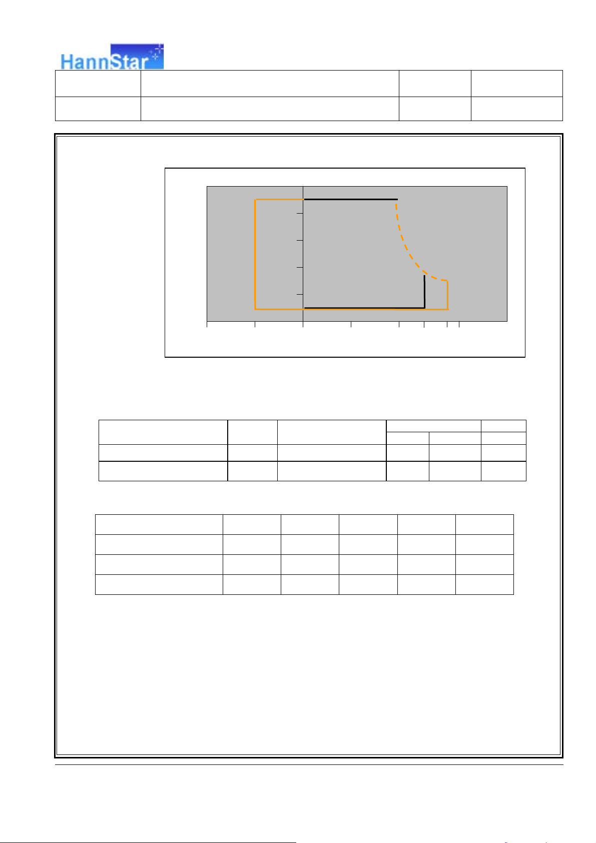
Humidity (%)
100
90
80
60
40
Storage Range
20
10
0
-20-40
Operating Range
0
Temperature (
20 40 60
o
C)
50
65
2.2 Electrical Absolute Rating:
2.2.1 TFT LCD Module:
Item Symbol Condition
Input Power Voltage
Logic Signal input voltage
2.2.2 Back Light Unit:
V
DD
V
SIG
Normal
Normal -0.3
Value Unit
min. max.
+3.0 +3.8
V
+0.3
DD
V(DC)
V
Item Symbol Min. Max. Unit Note
Lamp voltage
Lamp current
Lamp frequency f
V
L
I
L
L
0 2000 V(rms) (1)
-
9.0 mA (1)
0 100 KHz (1)
Note: (1) Permanent damage may occur to the LCD module if beyond this specification.
Functional operation should be restricted to the conditions described under
Normal Operating Conditions.
The information contained in this document is the exclusive property of HannStar Display Corporation. It shall not be
disclosed, distributed or reproduced in whole or in part without written permission of HannStar Display Corporation.
Page 7
HannStar Display Corp.
Document Title HSD150SX87 Product Information Page No.
Document No. Revision 1.0
7 / 28
3.0 OPTICAL CHARACTERISTICS
3.1 Measuring Condition
■ Measuring surrounding : dark room
■ Lamp current I
■ V
=3.3V, fV=60Hz, f
DD1
■ Surrounding temperature : 25±2
■ 30min. Warm-up time.
3.2 Measuring Equipment
■ LCD-7000 of Otsuka Electric Corp., which utilized MCPD-7000 for Chromaticity
and BM-5A for other optical characteristics.
■ Measuring spot size : 10~12mm
3.3 Optical specification
Item Symbol Condition Min. Typ. Max. Unit Note
Contrast CR 300 450 -- (1)(2)
Response time
White luminance
(center of screen)
Color
chromaticity
(CIE1931)
Viewing angle
Brightness uniformity B
: (8.0)±0.1mA, lamp freq. FL=55 KHz
BL
=32.5MHz
DCLK
o
C
Rising
TR +TF -- 16 -- msec (1)(3)
Falling
200 250 cd/m
o
0.604 0.634 0.664
0.309 0.339 0.369
0.255 0.285 0.315
0.557 0.587 0.617
0.114 0.144 0.174
Red
Green
Y
Rx
Ry
Gx
Gy
Bx
L
Θ=0
o
φ=0
Normal
viewing
angle
Blue
By
Wx
0.045 0.075 0.105
0.28 0.31 0.34
White
0.3 0.33 0.36
-- 65 --
-- 65 --
-- 45 --
-- 55 --
-- 75 --
-- 75 --
-- 50 --
-- 65 --
75 -- -- % (5)
Hor.
Ver.
Hor.
Ver.
Wy
Θ
Θ
Θ
Θ
Θ
Θ
Θ
Θ
UNI
L
R
CR>10
H
L
L
R
H
L
CR>5
Θ=0
φ=0
o
o
2
(1)
(1)(4)
The information contained in this document is the exclusive property of HannStar Display Corporation. It shall not be
disclosed, distributed or reproduced in whole or in part without written permission of HannStar Display Corporation.
Page 8
HannStar Display Corp.
Document Title HSD150SX87 Product Information Page No.
Document No. Revision 1.0
8 / 28
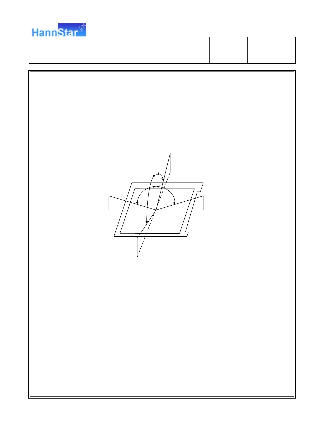
Note (1) Definition of Viewing Angle:
Φ
H
12’ o’clock
o
R
Θ
ΦH=90
L
Θ
ΘL=90
o
Φ
L
6’ o’clock
ΦL=90
Note (2) Definition of Contrast Ratio(CR) :
measured at the center point of panel
Luminance with all pixels white (L63)
CR =
Luminance with all pixels black (L0)
o
ΘR=90
o
The information contained in this document is the exclusive property of HannStar Display Corporation. It shall not be
disclosed, distributed or reproduced in whole or in part without written permission of HannStar Display Corporation.
Page 9
HannStar Display Corp.
Document Title HSD150SX87 Product Information Page No.
9 / 28
Document No. Revision 1.0
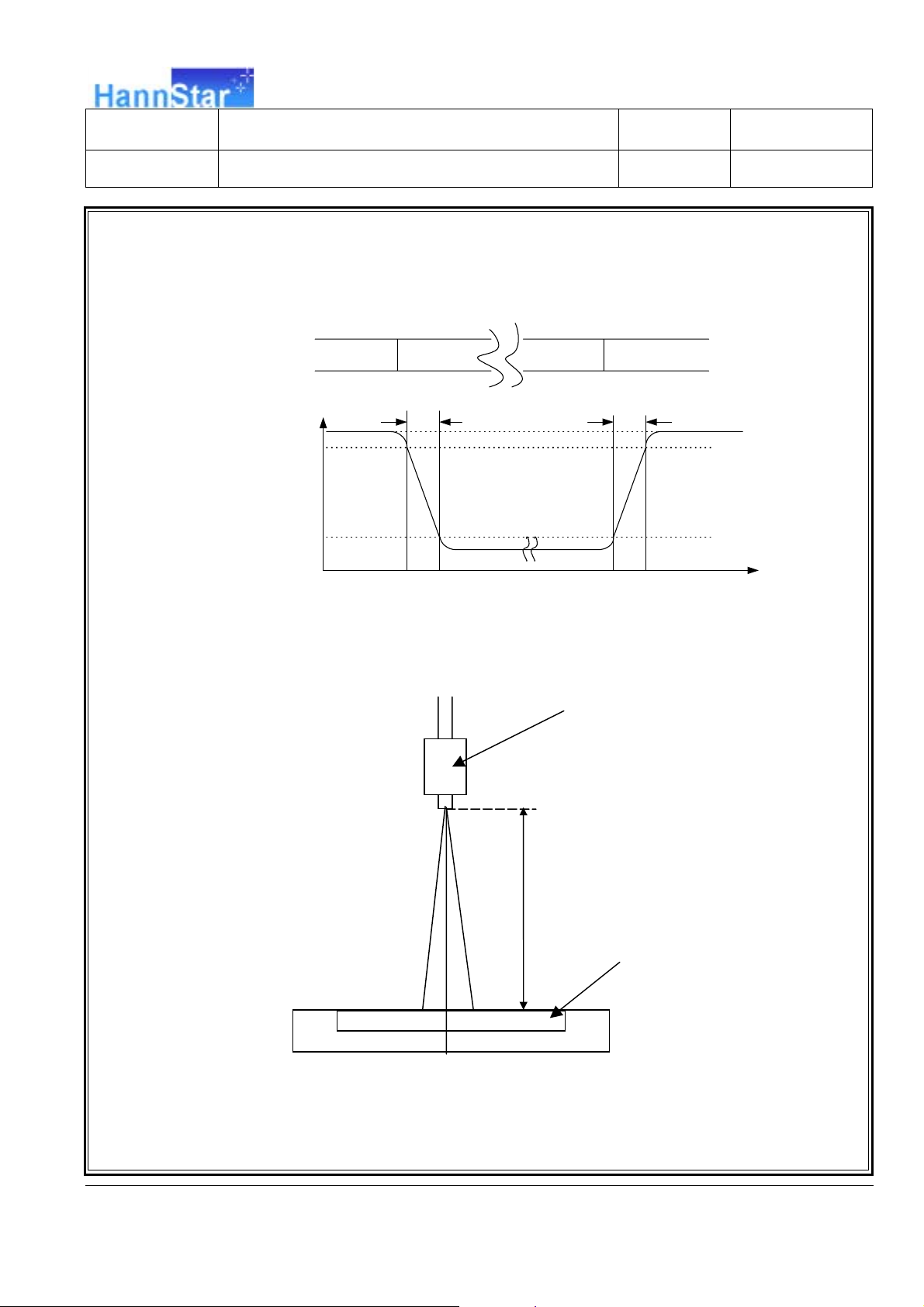
Note (3) Definition of Response Time: Sum of TR and T
white(TFT OFF) black (TFT ON) white(TFT OFF)
T
R
100%
90%
F
T
F
Optical
response
10%
0%
time
Note (4) Optical characteristic measurement setup
Field=2
o
50cm
Photo-detector (BM-5A)
LCD panel
The information contained in this document is the exclusive property of HannStar Display Corporation. It shall not be
disclosed, distributed or reproduced in whole or in part without written permission of HannStar Display Corporation.
Page 10

HannStar Display Corp.
Document Title HSD150SX87 Product Information Page No.
10 / 28
Document No. Revision 1.0
Note (5) Definition of brightness uniformity
Luminance uniformity =(Min Luminance)/(Max Luminance) x 100%
1
-
V
4
V
1
-
V
2
1
-
V
4
Display center
1
-
H
4
1
-
H
2
H
1
-
H
4
The information contained in this document is the exclusive property of HannStar Display Corporation. It shall not be
disclosed, distributed or reproduced in whole or in part without written permission of HannStar Display Corporation.
Page 11

HannStar Display Corp.
Document Title HSD150SX87 Product Information Page No.
Document No. Revision 1.0
11 / 28
4.0 BLOCK DIAGRAM
4.1 LCD Module Block Diagram:
X-Y FPC
(LCM Internal connector)
X-Y
Connector
Interface
Connector
(J2)
40
Interface
Connector
(J1)
140
DC-DC
1
Voltage
Reference
Circuit
X-PCB
Common
Voltage
Circuit
Drivers
Source
Gate
Drivers
Y-PCB
LCD Panel
768 lines x 1024 pixels
The information contained in this document is the exclusive property of HannStar Display Corporation. It shall not be
disclosed, distributed or reproduced in whole or in part without written permission of HannStar Display Corporation.
Page 12

HannStar Display Corp.
Document Title HSD150SX87 Product Information Page No.
Document No. Revision 1.0
12 / 28
4.2 Pixel Format
1st Pixel 2nd Pixel 3rd Pixel 4th Pixel 5th Pixel 6th Pixel 1024th Pixel
1st Line
2nd Line
3rd Line
4th Line
5th Line
6th Line
R G B R G B R G B R G B R G B R G B R G B
R G B R G B R G B R G B R G B R G B
R G B R G B R G B R G B R G B
R G B R G B R G B R G B
R G B R G B R G B
R G B R G B
R G B R G B R G B R G B R G B
R G B R G B R G B
R G B R G B R G B R G B
R G B
R G B R G B
768th Line
LCD Display Area
1 Pixel =
R G B R G B R G B R G B R G B R G B R G B
1024 Pixels
R G B
768 Lines
The information contained in this document is the exclusive property of HannStar Display Corporation. It shall not be
disclosed, distributed or reproduced in whole or in part without written permission of HannStar Display Corporation.
Page 13

HannStar Display Corp.
Document Title HSD150SX87 Product Information Page No.
13 / 28
Document No. Revision 1.0
4.3 Relationship between Displayed Color and Input Data
Basic
color
Gray
scale
of
Red
Gray
scale
of
Green
Gray
scale
of
Blue
Gray
scale
of
White
and
Black
Display
BlackLLLLLLLLLLLLLLLLLL -
Blue LLLLLLLLLLLLHHHHHH -
GreenLLLLLLHHHHHHLLLLLL -
Light BlueLLLLLLHHHHHHHHHHHH -
Red HHHHHHLLLLLLLLLLLL -
PurpleHHHHHHLLLLLLHHHHHH -
YellowHHHHHHHHHHHHLLLLLL -
White HHHHHHHHHHHHHHHHHH -
BlackLLLLLLLLLLLLLLLLLL L0
Dark
Light
Red HHHHHHLLLLLLLLLLLLRed L63
BlackLLLLLLLLLLLLLLLLLL L0
Dark
Light
GreenLLLLLLHHHHHHLLLLLLGreen L63
BlackLLLLLLLLLLLLLLLLLL L0
Dark
Light
Blue LLLLLLLLLLLLHHHHHHBlue L63
BlackLLLLLLLLLLLLLLLLLL L0
Dark
Light
White HHHHHHHHHHHHHHHHHHWhite L63
MSB LSB
R5 R4 R3 R2 R1 R0
LLLLLHLLLLLLLLLLLL L1
LLLLHLLLLLLLLLLLLL L2
↑
↓
HHHHLHLLLLLLLLLLLL L61
HHHHHLLLLLLLLLLLLL L62
LLLLLLLLLLLHLLLLLL L1
LLLLLLLLLLHLLLLLLL L2
↑
↓
LLLLLLHHHHLHLLLLLL L61
LLLLLLHHHHHLLLLLLL L62
LLLLLLLLLLLLLLLLLH L1
LLLLLLLLLLLLLLLLHL L2
↑
↓
LLLLLLLLLLLLHHHHLH L61
LLLLLLLLLLLLHHHHHL L62
LLLLLHLLLLLHLLLLLH L1
LLLLHLLLLLHLLLLLHL L2
↑
↓
HHHHLHHHHHLHHHHHLH L61
HHHHHLHHHHHLHHHHHL L62
:
:
:
:
:
:
:
:
MSB LSB
G5 G4 G3 G2G1 G0
:
:
:
:
:
:
:
:
MSB LSB
B5 B4 B3 B2 B1 B0
:
:
:
:
:
:
:
:
Gray scale
L3…L60
L3…L60
L3…L60
L3…L60
level
The information contained in this document is the exclusive property of HannStar Display Corporation. It shall not be
disclosed, distributed or reproduced in whole or in part without written permission of HannStar Display Corporation.
Page 14

HannStar Display Corp.
Document Title HSD150SX87 Product Information Page No.
14 / 28
Document No. Revision 1.0
5.0 I/O CONNECTION PIN ASSIGNMENT
5.1 Interface FPC Connector (40-pins x 2) (Hirose: FH12-40S-0.5SH)
I/F FRC Connector (J1) I/F FRC Connector (J2)
Pin
Symbol Description
No.
1
NC No Connecting
2
NC No Connecting
3
GND Ground
4
GND Ground
5
EB5 Even-dot Blue Data bit 5 (MSB)
6
EB4 Even-dot Blue Data bit 4
7
EB3 Even-dot Blue Data bit 3
8
EB2 Even-dot Blue Data bit 2
9
EB1 Even-dot Blue Data bit 1
10
EB0 Even-dot Blue Data bit 0 (LSB)
11
GND Ground
12
EG5 Even-dot Green Data bit 5 (MSB)
13
EG4 Even-dot Green Data bit 4
14
EG3 Even-dot Green Data bit 3
15
EG2 Even-dot Green Data bit 2
16
EG1 Even-dot Green Data bit 1
17
EG0 Even-dot Green Data bit 0 (LSB)
18
GND Ground
19
ER5 Even-dot Red Data bit 5 (MSB)
20
ER4 Even-dot Red Data bit 4
21
ER3 Even-dot Red Data bit 3
22
ER2 Even-dot Red Data bit 2
23
ER1 Even-dot Red Data bit 1
24
ER0 Even-dot Red Data bit 0 (LSB)
25
GND Ground
26
CPH1 Pixel Clock Input
27
GND Ground
28
GND Ground
29
STH Horizontal Start Pulse
30
LOAD Source Driver Latch Pulse
31
POL Source Driver Output Polarity control
32
REV Data Reverse Control Signal
33
GND Ground
34
GND Ground
35
STV Vertical Start Pulse
36
NC No Connecting
37
CPV Vertical Clock Input
38
OE Gate Driver Output Enable Signal
39
GND Ground
40
GND Ground
Pin
Symbol Description
No.
1
VDD Digital Power Input (DC +3.3V)
2
VDD Digital Power Input (DC +3.3V)
3
GND Ground
4
GND Ground
5
OB5 Odd-dot Blue Data bit 5 (MSB)
6
OB4 Odd-dot Blue Data bit 4
7
OB3 Odd-dot Blue Data bit 3
8
OB2 Odd-dot Blue Data bit 2
9
OB1 Odd-dot Blue Data bit 1
10
OB0 Odd-dot Blue Data bit 0 (LSB)
11
GND Ground
12
OG5 Odd-dot Green Data bit 5 (MSB)
13
OG4 Odd-dot Green Data bit 4
14
OG3 Odd-dot Green Data bit 3
15
OG2 Odd-dot Green Data bit 2
16
OG1 Odd-dot Green Data bit 1
17
OG0 Odd-dot Green Data bit 0 (LSB)
18
GND Ground
19
OR5 Odd-dot Red Data bit 5 (MSB)
20
OR4 Odd-dot Red Data bit 4
21
OR3 Odd-dot Red Data bit 3
22
OR2 Odd-dot Red Data bit 2
23
OR1 Odd-dot Red Data bit 1
24
OR0 Odd-dot Red Data bit 0 (LSB)
25
GND Ground
26
CPH2 Pixel Clock Input
27
GND Ground
28
GND Ground
29
NC No Connecting
30
NC No Connecting
31
NC No Connecting
32
NC No Connecting
33
NC No Connecting
34
NC No Connecting
35
NC No Connecting
36
NC No Connecting
37
NC No Connecting
38
NC No Connecting
39
GND Ground
40
GND Ground
The information contained in this document is the exclusive property of HannStar Display Corporation. It shall not be
disclosed, distributed or reproduced in whole or in part without written permission of HannStar Display Corporation.
Page 15

HannStar Display Corp.
Document Title HSD150SX87 Product Information Page No.
Document No. Revision 1.0
5.2
Back Light Unit (CCFL) Connectors:
15 / 28
CN3
CN4
CN3, 4:
Mating connector
Terminal No. Symbol Function
Note 1) Please connects NC pin to nothing. Don’t connect it to ground nor to other signal
Input. (NC pin should be open.)
CCFL Power Source (BHR-03VS-1/Japan Solderless Terminal MFG Co., LTD)
:
SM02 (8.0)B-BHS-1/ Japan Solderless Terminal MFG Co., LTD
1 VL CCFL power supply (high voltage)
2NC
3GL
1)
No connection
CCFL power supply (low voltage)
The information contained in this document is the exclusive property of HannStar Display Corporation. It shall not be
disclosed, distributed or reproduced in whole or in part without written permission of HannStar Display Corporation.
Page 16

HannStar Display Corp.
Document Title HSD150SX87 Product Information Page No.
Document No. Revision 1.0
6.0 ELECTRICAL CHARACTERISTICS
6.1 Electrical System of LCD Module:
Value
Item Symbol Condition
Min. Typ. Max.
Input Voltage
Input
Rush Current
Input Signal
voltage
V
DD
Irush
V
IH
V
IL
VDD = +3.3V
Each Iout = max.
High Level
Low Level
+3.0 +3.3 +3.6
1.5(*)
2.4 3.3 VDD+0.2
0
-
0.9
* Inrush current conditions
16 / 28
Unit
V(DC)
A
V
V
3.3V
6.2 Back-Light Unit:
The backlight system is an edge-lighting type with 2-CCFL (Cold Cathode Fluorescent Lamp).
The characteristics of four lamps are shown in the following tables.
Item Symbol Min. Typ. Max. Unit Note
Lamp current I
Lamp voltage V
Frequency f
Lamp life time Hr 30,000 --
t=400us ~ 10ms
L
L
L
4.0 8.0 9.0 mA(rms) (1)
640 670 700 V(rms) IL=8.0 mA
45 55 80 KHz (2)
-
Hour (3)
1400 at 25oC
Startup voltage Vs
1050
--
V(rms)
at 0oC
The information contained in this document is the exclusive property of HannStar Display Corporation. It shall not be
disclosed, distributed or reproduced in whole or in part without written permission of HannStar Display Corporation.
Page 17

HannStar Display Corp.
Document Title HSD150SX87 Product Information Page No.
Document No. Revision 1.0
17 / 28
Note: (1) Lamp current is measured with current meter for high frequency as shown below.
Specified values are for a lamp.
1
2
3
A
INVERTER
LCD MODULE
1
2
3
A
(HIU-766)
(2) Lamp frequency may produce interference with horizontal synchronous frequency and this
may cause line flow on the display. Therefore lamp frequency shall be detached from the
horizontal synchronous frequency and its harmonics as far as possible in order to avoid
interference.
(3) Life time (Hr) can be defined as the time in which it continues to operate under the condition:
Temp. =25±3ºC, IL=8.0mA(rms.) and fL=55 KHz until one of the following event occurs:
1.When the brightness becomes 50%.
2.When the startup voltage (Vs) at 0ºC becomes higher than the maximal value of Vs
specified above.
The information contained in this document is the exclusive property of HannStar Display Corporation. It shall not be
disclosed, distributed or reproduced in whole or in part without written permission of HannStar Display Corporation.
Page 18

HannStar Display Corp.
Document Title HSD150SX87 Product Information Page No.
Document No. Revision 1.0
18 / 28
6.3 AC Electrical Characteristics:
6.3.1 AC Timing: (VDD1=3.0V~3.6V, TOPR=25 oC) 5)
Item Symbol Min. Typ. Max. Unit Signals Note
Reference
Signal
(Pixel Clock)
Reference
Signal
(DENB)
Vertical
Periodic
Horizontal
Periodic
Periodic
Line Periodic
Line Active
Line Blank
Frame
Periodic
Frame Active
Frame Blank
Periodic
Pulse Width
Set-up Time
Hold Time
Period
Pulse Width
Rising Time
Falling Time
Set-up Time
Hold Time
F1
T1=CLK
T2=T1*2
T3=Line 526 672 900 T2
T4 512 512 512 T2
T5 14 160 388 T2
T6 773 806 950 Lines
T7 768 768 768 Lines
T8 5 --- --- Lines
T6 773 806 950 Lines
T9 1 1 --- Lines
T13 700 800 --- n-Sec
T14 700 800 --- n-Sec
T15 --- 1 --- Lines
T16A
T16B
T16C
T16D
T17A
T17B
T17C
T17D
T18A
T18B
T18C
T18D
T19A
T19B
T20A
T20B
50
12.5
25
1
1
2
25
2
2
2
2
7
7
7
7
65
15.384
30.769
64
30.769
40
40
4
4
40
40
4
4
10
10
10
10
80
20
40
100
40
60
60
60
60
--- n-Sec
--- n-Sec
MHz
n-Sec
n-Sec
u-Sec
u-Sec
T2
n-Sec
n-Sec
n-Sec
STV
OE
CPV
LOAD
STH
LOAD
STH
1), 2), 4)
2)
The information contained in this document is the exclusive property of HannStar Display Corporation. It shall not be
disclosed, distributed or reproduced in whole or in part without written permission of HannStar Display Corporation.
Page 19

HannStar Display Corp.
Document Title HSD150SX87 Product Information Page No.
Document No. Revision 1.0
19 / 28
Item Symbol Min. Typ. Max. Unit Signals Note
T21 --- 2 --- Lines
T22 --- 1 --- Lines
T23 --- --- 8 n-Sec
T24 --- --- 8 n-Sec
T25 6 --- --- n-Sec
T26 2 --- --- n-Sec
T2 25.00 30.769 40 n-Sec
T27 --- --- 8 n-Sec
T28 --- --- 8 n-Sec
POL
CPH1
CPH2
6Horizontal
Periodic
Clock
Period
Pulse Width
Rising Time
Falling Time
Set-up Time
Hold Time
Period
Rising Time
Falling Time
ER(5:0)
Image Data
And
Data
Reverse
Control Pin
Setup time
Hold time
T29 6 --- --- n-Sec
T30 2 --- --- n-Sec
EG(5:0)
EB(5:0)
OR(5:0)
OG(5:0)
OB(5:0)
REV
Relative
Signals
LOAD rising-
STH rising
CPV rising-
LOAD rising
T31 6 --- --- T2
T32 3.5 3.7 4.5 u-Sec
Frame Rate Recommend using :
3)
V signals F
H signals F
V
H
---
60.00 85 Hz 6)
39.5 48.35 70 KHz
Note 1) Refer to VESA standard.
Note 2) In case of using the long frame period, the deterioration of display quality, noise etc.
may be occurred.
Note 3) Do not fix CPH1 and CPH2 to “H” or “L” level while the VDD (+3.3V) is supplied. If
CPH1 and CPH2 is fixed to “H” level or “L” level for certain period while the V
DD
(+3.3V) is supplied, the panel may be damaged.
Note 4) Do not change t3 and t6 values in the operation. When t1 or t4 is changed, the panel
is displayed as black.
The information contained in this document is the exclusive property of HannStar Display Corporation. It shall not be
disclosed, distributed or reproduced in whole or in part without written permission of HannStar Display Corporation.
Page 20

HannStar Display Corp.
Document Title HSD150SX87 Product Information Page No.
Document No. Revision 1.0
20 / 28
Note 5) Please adjust LCD operating signal timing and FL driving frequency, to optimize the
display quality. There is a possibility that flicker is observed by the interference of
LCD operating signal timing and FL driving condition (especially driving frequency).
Note 6) All of the timing have to meet “ 6.3.1 AC timing chart – Pixel frequency must less than
40MHz“, frame rate 85Hz can be acceptable.
6.3.2 AC Timing Charts:
(1). Reference Signal (pixel clock):
Reference Signal
(Pixel Clock)
Input Clock
T1
F1=1/T1
T2
The information contained in this document is the exclusive property of HannStar Display Corporation. It shall not be
disclosed, distributed or reproduced in whole or in part without written permission of HannStar Display Corporation.
Page 21

HannStar Display Corp.
Document Title HSD150SX87 Product Information Page No.
21 / 28
Document No. Revision 1.0
(2). Vertical Periodic (STV1, STV2, OE, CPV):
T7 T8 T6
DENB
(For Reference)
STV
OE
CPV
LOAD
STH
DENB
(For Reference)
STV
OE
CPV
LOAD
STH
POL
T32
T23
T24
T16A
T3
T9
T13 T14
T16C
T21
T4 T5
T12T11
T16B
T17C
T15
T17A
T17B T18B
T22
T18A
T18C
+
The information contained in this document is the exclusive property of HannStar Display Corporation. It shall not be
disclosed, distributed or reproduced in whole or in part without written permission of HannStar Display Corporation.
Page 22

HannStar Display Corp.
Document Title HSD150SX87 Product Information Page No.
22 / 28
Document No. Revision 1.0
(3). Horizontal Periodic 1 (STH, CPH, DATA):
T27 T28
CPH1
CPH2
STH
Odd R,G,B Data
Even R,G,B Data
70%
30%
70%
30%
INVALID
INVALID
50%
50%
50%
T16D
50%
50%
th
5
Pixel
th
6
Pixel
T2
7
Pixel
8
Pixel
th
th
9
Pixel
th
10
Pixel
th
11
Pixel
th
th
12
Pixel
1023
1024
T20BT19B
T30T29
st
1
Pixel
2
Pixel
rd
3
Pixel
nd
th
4
Pixel
th
Pixel
th
Pixel
REV
INVALID
(4). Horizontal Periodic 2 (CPH, LOAD, STH, POL):
CPH1
CPH2
LOAD
STH
POL
70%
30%
70%
30%
50%
T25
50%
50%
T19A
T20A
50%
T31
50%
50%
T16C
T17D T18D
70%
50%
30%
T2
50%
T26
50%
The information contained in this document is the exclusive property of HannStar Display Corporation. It shall not be
disclosed, distributed or reproduced in whole or in part without written permission of HannStar Display Corporation.
Page 23

HannStar Display Corp.
Document Title HSD150SX87 Product Information Page No.
Document No. Revision 1.0
(5). Initial Condition:
Power ON
0.9 VDD
VDD
(3.3V)
0V
100 ms
Dat a &
23 / 28
Control signal s
40 ms
OE
* Input Power (VDD) should be 0V(GND) before Power-ON.
* All signals (including control signals and data) should be kept low
before it is active.
The information contained in this document is the exclusive property of HannStar Display Corporation. It shall not be
disclosed, distributed or reproduced in whole or in part without written permission of HannStar Display Corporation.
Page 24

HannStar Display Corp.
Document Title HSD150SX87 Product Information Page No.
Document No. Revision 1.0
6.4 Power On / Off Sequence:
Power On
Power Off
24 / 28
Power Supply
0V
0V
0.1V
Signal
0.9V
DD
TP1
TP2
0.6V 0.6V
TP3
0.9V
0.1V
DD
TP4
0.1V
DD
TP5
TP6
Backlight
(Recommended)
50%
50%
Item Min. Typ. Max. Unit Remark
TP1 0.4
TP2 100
TP3 0
TP4 1
TP5 200
TP6 200
-
-
-
--
--
--
10 msec
200 msec
50 msec
sec
msec
msec
Note:(1) The supply voltage of the external system for the module input should be the same as the
definition of VDD.
(2) Apply the lamp volatge within the LCD operation range. When the back-light turns on
before the LCD operation or the LCD truns off before the back-light turns off, the display
may momentarily become white.
(3) In case of VDD = off level, please keep the level of input signal on the low or keep a high
impedance.
(4) T4 should be measured after the module has been fully discharged between power off and
on period.
(5)Interface signal shall not be kept at high impedance when the power is on.
The information contained in this document is the exclusive property of HannStar Display Corporation. It shall not be
disclosed, distributed or reproduced in whole or in part without written permission of HannStar Display Corporation.
Page 25

HannStar Display Corp.
Document Title HSD150SX87 Product Information Page No.
Document No. Revision 1.0
7.0 Suggested Timing (VESA – 1024x768/60Hz) :
Vertical Blanking
DE
1 horizontal period = 20.67us
STV1
1/2 horizontal period = 10.33us
25 / 28
STV2
STH
OE
CPV
LOAD
768th line
41.34us
4.69us
3.68us
1/2 horizontal period=10.33us
1 horizontal period = 20.67us
3.68us
16.99us
1 horizontal period = 20.67us
1.84us
At least 3 pulses after the last line
The information contained in this document is the exclusive property of HannStar Display Corporation. It shall not be
disclosed, distributed or reproduced in whole or in part without written permission of HannStar Display Corporation.
Page 26

HannStar Display Corp.
Document Title HSD150SX87 Product Information Page No.
Document No. Revision 1.0
26 / 28
CPH
15.4 ns
1 horizontal period = 20.67us
LOAD
1.84us
STH
4.69us
122.8ns
30.7ns
POL
The information contained in this document is the exclusive property of HannStar Display Corporation. It shall not be
disclosed, distributed or reproduced in whole or in part without written permission of HannStar Display Corporation.
Page 27

HannStar Display Corp.
Document Title HSD150SX87 Product Information Page No.
27 / 28
Document No. Revision 1.0
8.0 OUTLINE DIMENSION
8.1 Front View: Date: 2003.02.26
HannStar DISPLAY CORP.
The information contained in this document is the exclusive property of HannStar Display Corporation. It shall not be
disclosed, distributed or reproduced in whole or in part without written permission of HannStar Display Corporation.
Page 28

HannStar Display Corp.
Document Title HSD150SX87 Product Information Page No.
28 / 28
Document No. Revision 1.0
8.2 Back View: Date: 2003.02.26
HannStar DISPLAY CORP.
The information contained in this document is the exclusive property of HannStar Display Corporation. It shall not be
disclosed, distributed or reproduced in whole or in part without written permission of HannStar Display Corporation.
 Loading...