

Page 1
HannStar Display Corp.
Document Title HSD150PX17 Product Information Page No. 1 / 31
Document No. Revision 1.0
HannStar Product Information
Model : HSD150PX17
-A00
(A00: sub model code)
Note:1.Please contact HannStar Display Corp. before designing your product based on this module
specification.
2.The information contained herein is presented merely to indicate the characteristics and perfor mance of our products. No responsibility is assumed by HannStar for any intellectual property
claims or other problems that may result from application based on the module described herein.
The information contained in this document is the exclusive property of HannStar Display Corporation. It shall not be
disclosed, distributed or reproduced in whole or in part without written permission of HannStar Display Corporation.
Page 2
HannStar Display Corp.
Document Title HSD150PX17 Product Information Page No. 2 / 31
Document No. Revision 1.0
Record of Revisions
Rev. Date Description of change
1.0
HSD150PX17-A00 formal specification was first issued..
The information contained in this document is the exclusive property of HannStar Display Corporation. It shall not be
disclosed, distributed or reproduced in whole or in part without written permission of HannStar Display Corporation.
Page 3
HannStar Display Corp.
Document Title HSD150PX17 Product Information Page No. 3 / 31
Document No. Revision 1.0
Contents
1.0 General description ……………………………….… p.4
2.0 Absolute maximum ratings …………………………. p.6
3.0 Optical characteristics ………………………………. p.8
4.0 Block diagram …………………………….. ……….. p.13
5.0 Interface pin connection ……………………………. p.17
6.0 Electrical characteristics ……………………………. p.18
7.0 Outline dimension …………………………………… p.25
8.0 Lot mark …………………………….………………… p.28
9.0 Package specification ………………………………. p.29
10.0 General precaution ………………………………….. p.31
The information contained in this document is the exclusive property of HannStar Display Corporation. It shall not be
disclosed, distributed or reproduced in whole or in part without written permission of HannStar Display Corporation.
Page 4
HannStar Display Corp.
Document Title HSD150PX17 Product Information Page No. 4 / 31
Document No. Revision 1.0
1.0 GENERAL DESCRIPTION
1.1 Introduction
HannStar Display model HSD150PX17-A is a color active matrix thin film transistor (TFT)
liquid crystal display(LCD) that uses amorphous silicon TFT as a switching device. This
model is composed of a TFT LCD panel, a driving circuit and a back light system. This
TFT LCD has a 15 inch diagonally measured active display area with XGA resolution
(768 vertical by 1024 horizontal pixel array) and can display up to 262,144 colors.
1.2 Features
■ 15” XGA for Notebook PC
■ LVDS interface.
■ SPWG style-B standard
■ High luminance
■ Input timing: DE mode
1.3 Applications
■ Notebook PC
■ Moniputers
■ Display terminals for AV applications
■ Monitors for industrial applications
1.4 General information
Item Specification Unit
Outline Dimension 317.3(H) x 242.0(V) x 6.0(max)
Display area 304.128(H) x 228.096(V) (15.0” diagonal) mm
Number of Pixel 1024(H) x 768(V) pixels
Pixel pitch 0.297(H) x 0.297(V) mm
Pixel arrangement RGB Vertical stripe
Display color 262,144 colors
Display mode Normally white
Surface treatment Antiglare, Hard-Coating(3H)
Weight 560 (Typ.) g
Back-light Single CCFL (Side-Light type)
Input signal 1-ch LVDS with EDID(following SPWG)
The information contained in this document is the exclusive property of HannStar Display Corporation. It shall not be
disclosed, distributed or reproduced in whole or in part without written permission of HannStar Display Corporation.
Page 5
HannStar Display Corp.
Document Title HSD150PX17 Product Information Page No. 5 / 31
Document No. Revision 1.0
1.5 Mechanical Information
Item Min. Typ. Max. Unit
Horizontal(H) 316.8 317.3 317.8 mm
Module
Size
Vertical(V) 241.5 242.0 242.5 mm
Depth(D) --- --- 6.0 mm
Weight (Without inverter) --- 560 575 g
Torgue of custom screw hole --- --- 1.8 Kgf•Cm
The information contained in this document is the exclusive property of HannStar Display Corporation. It shall not be
disclosed, distributed or reproduced in whole or in part without written permission of HannStar Display Corporation.
Page 6
HannStar Display Corp.
Document Title HSD150PX17 Product Information Page No. 6 / 31
Document No. Revision 1.0
2.0 ABSOLUTE MAXIMUM RATINGS
2.1 Absolute Rating of Environment
Item Symbol Min. Max. Unit Note
Storage temperature T
Operating temperature T
Vibration(non-operating) V
Shock(non-operating) S
Storage humidity H
Operating humidity H
Low pressure(operating) P
Low pressure(non-operating) P
-20 60
STG
0 50
OPR
- 1.5 G (2)
NOP
180 - G (3)
NOP
10 90 %RH (3)
STG
10 80 %RH (4)
OP
697 - hPa (5)
LOP
116 - hPa (6)
LNOP
Note (1) Storage / Operating temperature
Humidity (%)
100
90
80
60
Operating Range
Storage Range
-20-40
40
20
10
0
0
Temperature (
20 40
o
C)
50
(2) 5-500-5Hz sine wave, X,Y,Z each directions, 30min/cycle.
(3)2ms, ±X, ±Y, ±Z direction, one time each. For this shock test, it is
necessary to fill the silicon rubber between the shock jig as buffer.
(4) Max wet bulb temp.=39
o
C
(5) 2hrs. (10000 feet)
(6) 24hrs. (50000 feet)
o
C
o
C (1)
60
The information contained in this document is the exclusive property of HannStar Display Corporation. It shall not be
disclosed, distributed or reproduced in whole or in part without written permission of HannStar Display Corporation.
Page 7
HannStar Display Corp.
Document Title HSD150PX17 Product Information Page No. 7 / 31
Document No. Revision 1.0
2.2 Electrical Absolute Rating
2.2.1 TFT LCD Module
Item Symbol Min. Max. Unit Note
Power supply voltage V
Logic input voltage V
2.2.2 Back-Light Unit
Item Symbol Min. Max. Unit Note
Lamp voltage V
Lamp current I
Lamp frequency f
Note (1) Permanent damage may occur to the LCD module if beyond this specification.
Functional operation should be restricted to the conditions described under
normally operating conditions.
(2) Within Ta =25±2℃
-0.3 4.0 V (1) (2)
DD
-0.3 VDD+0.3 V (1) (2)
IN
0 2000 V
FL
-- 8.0 mA (1) (2)
L
0 100 kHz (1) (2)
L
(1) (2)
(rms)
The information contained in this document is the exclusive property of HannStar Display Corporation. It shall not be
disclosed, distributed or reproduced in whole or in part without written permission of HannStar Display Corporation.
Page 8
HannStar Display Corp.
Document Title HSD150PX17 Product Information Page No. 8 / 31
Document No. Revision 1.0
3.0 OPTICAL CHARACTERISTICS
3.1 Optical specification
Item Symbol Condition Min. Typ. Max. Unit Note
Contrast CR
Response
time
White luminance
(Average of 5 points)
Color
chromaticity
(CIE1931)
Rising TR
Falling T
Red
Green
Blue
F
Y
Rx
R
Gx
G
Bx
B
L
Θ=0
Φ=0
y
Normal
viewing
y
y
angle
Wx
250 350
170 200
0.583 0.585 0.586
0.350 0.351 0.352
0.320 0.320 0.321
0.548 0.549 0.551
0.161 0.161 0.161
0.158 0.159 0.160
0.280 0.310 0.340
White
0.300 0.330 0.360
Viewing angle
(Min=Typ-5)
Hor.
Ver.
W
Θ
Θ
Θ
Θ
y
L
R
U
D
CR>10
-
-
35 40
35 40
15 20
35 40
7 13
15 20
-
-
-
-
-
-
(1)(2)
msec (1)(3)
cd/m2
(1)(4)(5)
(IL=6.0mA)
(1)(4)
Brightness uniformity B
Crosstalk CT(n)
UNI
Θ=0
Φ=0
65
- -
- -
1.3
% (6)
% (7)
3.2 Measuring Condition
■ Measuring surrounding : dark room
■ Lamp current I
■ V
=3.3V±0.05V
DD
■ Surrounding temperature : 25±2
: 6.0±0.1mA(rms), Lamp freq. F
FL
o
C
=50KHz, Inverter : HIU-757
L
■ 30min. Warm-up time.
The information contained in this document is the exclusive property of HannStar Display Corporation. It shall not be
disclosed, distributed or reproduced in whole or in part without written permission of HannStar Display Corporation.
Page 9
HannStar Display Corp.
Document Title HSD150PX17 Product Information Page No. 9 / 31
Document No. Revision 1.0
3.3 Measuring Equipment
■ Otsuka Electrics Corp., which utilized MCPD-7000 for Chromaticity
and BM-5 for other optical characteristics.
■ Measuring spot size : 10 ~ 12 mm
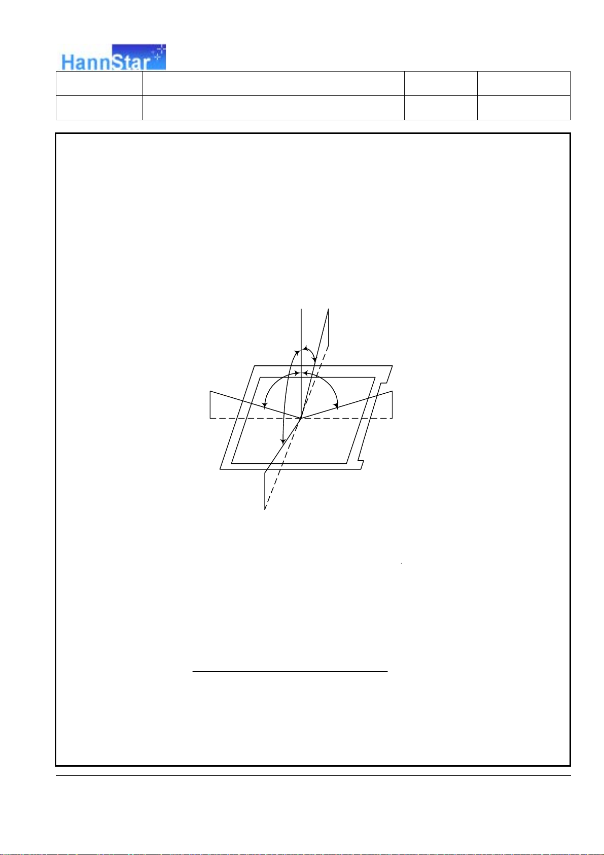
Note (1) Definition of Viewing Angle :
Θ
U
12’ o’clock
Φ=90
o
Φ=180
Θ
L
o
Θ
D
Θ
R
o
Φ=0
6’ o’clock
Φ=270
o
Note (2) Definition of Contrast Ratio(CR) :
measured at the center point of panel
Luminance with all pixels white (L63)
CR =
Luminance with all pixels black (L0)
The information contained in this document is the exclusive property of HannStar Display Corporation. It shall not be
disclosed, distributed or reproduced in whole or in part without written permission of HannStar Display Corporation.
Page 10
HannStar Display Corp.
Document Title HSD150PX17 Product Information Page No. 10 / 31
Document No. Revision 1.0
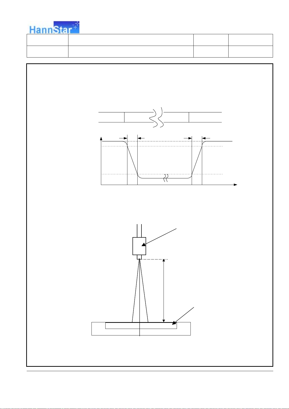
Note (3) Definition of Response Time : Sum of TR and TF
white(TFT OFF) black (TFT ON) white(TFT OFF)
100%
90%
T
R
T
F
Optical
response
10%
0%
time
Note (4) Definition of brightness uniformity
Photo-detector (BM-5A)
Field=2
o
50cm
LCD panel
Center of panel
The information contained in this document is the exclusive property of HannStar Display Corporation. It shall not be
disclosed, distributed or reproduced in whole or in part without written permission of HannStar Display Corporation.
Page 11

HannStar Display Corp.
Document Title HSD150PX17 Product Information Page No. 11 / 31
Document No. Revision 1.0
Note (5) Definition of Average Luminance of White (5 Point)
Y1+Y2+Y3+Y4+Y
Average Luminance =
10 mm
10 mm
256 512 768
Y
Y
2
Y
Y
4
Note (6) Definition of brightness uniformity
10 mm
5
Y1
5
10 mm
3
192
384
5
576
(Min Luminance of 13 points)
Luminance uniformity = ×100%
(Max Luminance of 13 points)
The information contained in this document is the exclusive property of HannStar Display Corporation. It shall not be
disclosed, distributed or reproduced in whole or in part without written permission of HannStar Display Corporation.
Page 12

HannStar Display Corp.
-
V
H
-
-
V
H
-
Document Title HSD150PX17 Product Information Page No. 12 / 31
Document No. Revision 1.0
Note (7) Definition of crosstalk CT(1) ~ CT(4)
L(n) – LB(n)
CT(n) = x 100% , n = 1 ~ 4
L(n)
Where L(n) = Luminance of point “n” at pattern A (cd/m
LB(n) = Luminance of point “n” at pattern B (cd/m
2
) , n=1∼4
2
) , n=1∼4
The location measured will be exactly the same in both patterns.
L0 : Luminance with all pixels black
L63 : Luminance with all pixels white
Gray scale: L31
Gray scale: L0
1
V
-
1
-
4
V
V
8
L(3)
1
-
V
1
4
V
8
1
-
H
8
1
-
4
1
-
2
L(1)
L(4)
1
-
V
2
L(2)
1
8
1
-
H
1
-
H
2
H
H
4
Pattern A Pattern B
1
-
1
-
-
V
8
V
4
1
V
1
4
V
8
-
Gray scale: L31
LB(1)
LB(3)
1
H
8
1
-
H
4
1
-
H
2
LB(2)
H
LB(4)
1
8
1
-
4
H
The information contained in this document is the exclusive property of HannStar Display Corporation. It shall not be
disclosed, distributed or reproduced in whole or in part without written permission of HannStar Display Corporation.
Page 13

HannStar Display Corp.
Document Title HSD150PX17 Product Information Page No. 13 / 31
Document No. Revision 1.0
4.0 BLOCK DIAGRAM
4.1 TFT LCD Module
X-driver IC
Timing
EDID
Connector
DC/DC
Converter
Controller
+
LVDS
Receiver
Y-driver IC
Liquid Crystal Panel
1024×768 pixels
4.2 Back Light Unit
Gray scale
Manipulation
Voltage
Generation
Circuit
1
2
The information contained in this document is the exclusive property of HannStar Display Corporation. It shall not be
disclosed, distributed or reproduced in whole or in part without written permission of HannStar Display Corporation.
VL
GL
Page 14

HannStar Display Corp.
Document Title HSD150PX17 Product Information Page No. 14 / 31
Document No. Revision 1.0
4.3 Pixel Format
1,1
1,2 1,3 1,4
2,1
768,
1
1,1024
LCD Display Area
1 Pixel
768,
1024
768 Lines
1024
R
G
R
R
B
The information contained in this document is the exclusive property of HannStar Display Corporation. It shall not be
disclosed, distributed or reproduced in whole or in part without written permission of HannStar Display Corporation.
Page 15

HannStar Display Corp.
Document Title HSD150PX17 Product Information Page No. 15 / 31
Document No. Revision 1.0
4.4 Relationship Between Displayed Color and Input
Basic
color
Gray
scale
of Red
Gray
scale of
Green
Gray
scale of
Blue
Gray
scale of
White &
Black
MSB LSB
Display
Black LLLLLLLLLLLLLLLLLL -
Blue LLLLLLLLLLLLHHHHHH -
Green L L L L L L H H H H H H L L L L L L -
Light Blue L L L L L L H H H H H H H H H H H H -
Red HHHHHHLLLLLLLLLLLL -
Purple HHHHHHL L L L L LHHHHHH -
Yellow HHHHHHHHHHHHL L L L L L -
White HHHHHHHHHHHHHHHHHH -
Black LLLLLLLLLLLLLLLLLL L0
Dark
Light
Red H H H H H H L L L L L L L L L L L L Red L63
Black LLLLLLLLLLLLLLLLLL L0
Dark
Light
Green L L L L L L H H H H H H L L L L L L Green L63
Black LLLLLLLLLLLLLLLLLL L0
Dark
Light
Blue L L L L L L L L L L L L H H H H H H Blue L63
Black LLLLLLLLLLLLLLLLLL L0
Dark
Light
White HHHHHHHHHHHHHHHHHHWhite L63
R5 R4 R3 R2 R1 R0
LLLLLHLLLLLLLLLLLL L1
LLLLHLLLLLLLLLLLLL L2
↑
↓
H H H H L H L L L L L L L L L L L L L61
H H H H H L L L L L L L L L L L L L L62
LLLLLLLLLLLHLLLLLL L1
LLLLLLLLLLHLLLLLLL L2
↑
↓
L L L L L L H H H H L H L L L L L L L61
L L L L L L H H H H H L L L L L L L L62
LLLLLLLLLLLLLLLLLH L1
LLLLLLLLLLLLLLLLHL L2
↑
↓
L L L L L L L L L L L L H H H H L H L61
L L L L L L L L L L L L H H H H H L L62
LLLLLHLLLLLHLLLLLH L1
LLLLHLLLLLHLLLLLHL L2
↑
↓
H H H H L H H H H H L H H H H H L H L61
H H H H H L H H H H H L H H H H H L L62
:
:
:
:
:
:
:
:
MSB LSB
G5 G4 G3 G2G1 G0
:
:
:
:
:
:
:
:
MSB LSB
B5 B4 B3 B2 B1 B0
:
:
:
:
:
:
:
:
Gray scale
L3…L60
L3…L60
L3…L60
L3…L60
level
The information contained in this document is the exclusive property of HannStar Display Corporation. It shall not be
disclosed, distributed or reproduced in whole or in part without written permission of HannStar Display Corporation.
Page 16

HannStar Display Corp.
Document Title HSD150PX17 Product Information Page No. 16 / 31
Document No. Revision 1.0
4.5 RECOMMENDED TRANSMITTER TO HSD150PX17-A INTERFACE ASSIGNMENT
Case1: DATA (6bit transmitter)
DS90CF363
Input Terminal No. Input Signal
(Graphics controller output signal)
Symbol Terminal Symbol Function
TIN0 44 R0 Red Pixels Display Data (LSB)
TIN1 45 R1 Red Pixels Display Data
TIN2 47 R2 Red Pixels Display Data
TIN3 48 R3 Red Pixels Display Data
TIN4 1 R4 Red Pixels Display Data
TIN5 3 R5 Red Pixels Display Data (MSB)
TIN6 4 G0 Green Pixels Display Data (LSB)
TIN7 6 G1 Green Pixels Display Data
TIN8 7 G2 Green Pixels Display Data
TIN9 9 G3 Green Pixels Display Data
TIN10 10 G4 Green Pixels Display Data
TIN11 12 G5 Green Pixels Display Data (MSB)
TIN12 13 B0 Blue Pixels Display Data (LSB)
TIN13 15 B1 Blue Pixels Display Data
TIN14 16 B2 Blue Pixels Display Data
TIN15 18 B3 Blue Pixels Display Data
TIN16 19 B4 Blue Pixels Display Data
TIN17 20 B5 Blue Pixels Display Data (MSB)
TIN18 22 NC Non Connection (open)
TIN19 23 NC Non Connection (open)
TIN20 25 ENAB Compound Synchronization Signal
CLK IN 26 NCLK Data Sampling Clock TCLK OUT-
Output Signal
Symbol
TOUT0-
TOUT0+
TOUT1-
TOUT1+
TOUT2-
TOUT2+
TCLK OUT+
LTM15C425S
Interface
(CN1)
Terminal Symbol
No.8
No.9
No.11
No.12
No.14
No.15
No.17
No.18
IN0-
IN0+
IN1-
IN1+
IN2-
IN2+
CLK-
CLK+
Note : Please connect NC pin to nothing. Don’t connect it to ground nor to other signal input.
IN 0
IN 1
IN 2
TIN6
G0
TIN13
B1
TIN20
ENA B
TIN5
R5
T IN 1 2 T IN 1 1 T IN 1 0 T IN 9 T IN 8
B0
T IN19 T IN18 T IN17 T IN16 T IN15
NC
The information contained in this document is the exclusive property of HannStar Display Corporation. It shall not be
disclosed, distributed or reproduced in whole or in part without written permission of HannStar Display Corporation.
TIN4 TIN3 TIN2 TIN1 TIN0
R4
G5
NC
R3 R2 R1 R0
TIN7
G4
B5
G3
B4
G2
G1
TIN14
B2B3
Page 17

HannStar Display Corp.
Document Title HSD150PX17 Product Information Page No. 17 / 31
Document No. Revision 1.0
5.0 INTERFACE PIN CONNECTION
5.1 TFT LCD Module
CN1 (INPUT SIGNAL): FI-XB30S-HF10 (JAE)
MATING CONNECTOR: FI-X30M,FI-X30MR
Terminal no. Symbol Function Note
1 GND Ground
2 VDD Power Supply : 3.3V(typical)
3 VDD Power Supply : 3.3V(typical)
4 VEDID DDC 3.3V power
5 NC Reserved for supplier test point
6 ClkEDID DDC clock
7 DATAEDID DDC data
8 IN0- - LVDS differential data input (R0-R5, G0) (2)
9 IN0+ + LVDS differential data input (R0-R5, G0) (2)
10 GND Ground
11 IN1- - LVDS differential data input (G1-G5, B0-B1) (2)
12 IN1+ + LVDS differential data input (G1-G5, B0-B1) (2)
13 GND Ground
14 IN2- - LVDS differential data input (B2-B5,DE) (2)
15 IN2+ + LVDS differential data input (B2-B5, DE) (2)
16 GND Ground
17 CLK- - LVDS differential clock input (2)
18 CLK+ + LVDS differential clock input (2)
19 GND Ground
20 NC Reserved for supplier test point (1)
21 NC Reserved for supplier test point (1)
22 GND Ground
23 NC Reserved for supplier test point (1)
24 NC Reserved for supplier test point (1)
25 GND Ground
26 NC Reserved for supplier test point (1)
27 NC Reserved for supplier test point (1)
28 GND Ground
29 NC Reserved for supplier test point (1)
30 NC Reserved for supplier test point (1)
Note (1) Please connects NC pin to nothing. Don’t connect it to ground nor to other signal input.
(NC pin should be open.)
Note (2) The module used a 100ohm resistor between positive and negative data lines of each
receiver input.
5.2 Back-Light Unit
CN2 CCFL Power Source (BHSR-02VS-1) / JAPAN SOLDERLESS TERMINAL MFG CO., LTD.
Mating Connector: (SBHT-002T-P0.5) / JAPAN SOLDERLESS TERMINAL MFG CO., LTD.
Terminal no. Symbol Function
1 VL CCFL power supply (high voltage)
2 GL CCFL power supply (low voltage)
The information contained in this document is the exclusive property of HannStar Display Corporation. It shall not be
disclosed, distributed or reproduced in whole or in part without written permission of HannStar Display Corporation.
Page 18

HannStar Display Corp.
Document Title HSD150PX17 Product Information Page No. 18 / 31
Document No. Revision 1.0
6.0 ELECTRICAL CHARACTERISTICS
6.1 TFT LCD Module
Item Symbol Min. Typ. Max. Unit Note
Voltage of power supply V
Current of power
supply
V-Color I
Mosaic I
Vsync frequency f
Hsync frequency f
Frequency f
Input rush current I
Note (1)
1). V-Color :
White
Yellow
Purple
2). Mosaic : Dot checker image
3.0 3.3 3.6 V
DD
DD1
DD2
--- 60 --- Hz (2)
V
--- 48.36 --- KHz
H
DCLK
--- --- 1.5 A (3)
Rush
Red
237 337 437
266 366 466
mA (1)
mA (1)
--- 65.00 --- MHz
Cyan
Green
Blue
Black
L7
Grey scale: L0∼L63.
L0: Luminance with all pixels black.
L63: Luminance with all pixels white.
The information contained in this document is the exclusive property of HannStar Display Corporation. It shall not be
disclosed, distributed or reproduced in whole or in part without written permission of HannStar Display Corporation.
L0
Page 19

HannStar Display Corp.
Document Title HSD150PX17 Product Information Page No. 19 / 31
Document No. Revision 1.0
Note (2) When fv is too low, a flicker may be occurred on the display.
Note (3) Input Rush Current condition
0.1VDD
GND
0.9VDD
3.3V
470us~10ms
The information contained in this document is the exclusive property of HannStar Display Corporation. It shall not be
disclosed, distributed or reproduced in whole or in part without written permission of HannStar Display Corporation.
Page 20

HannStar Display Corp.
Document Title HSD150PX17 Product Information Page No. 20 / 31
Document No. Revision 1.0
6.2 Back-Light Unit
The back-light system is an edge-lighting type with 1 CCFL
The characteristics of the lamp is shown in the following tables.
Item Symbol Min. Typ. Max. Unit Note
Lamp current IL 3.0 6.0 7.0 mA(rms) (1)
Lamp voltage VL 580 640 700 V(rms) I
Frequency fL 40 50 80 KHz (2)
Operating lamp life time Hr 10,000 -- -- Hour (3)
Startup voltage Vs
1250 at 25
1600
Note (1) Lamp current is measured with current meter for high frequency as shown
below. Specified valued are for a lamp.
(Cold Cathode Fluorescent Lamp).
L
-- -- V(rms)
=6.0mA
o
C
o
C
at 0
LCD MODULE
RED
WHITE(Ground)
Note (2) Lamp frequency may produce interference with horizontal synchronous
frequency and this may cause line flow on the display. Therefore lamp
frequency shall be detached from the horizontal synchronous frequency
and its harmonics as far as possible in order to avoid interference.
Note (3) Lamp life time (Hr) can be defined as the time in which it continues to operate
under the condition : Ta=25±3
o
C, IL=6.0mA(rms) and fL=50kHz until
one of the following event occurs :
1. When the brightness becomes 50%
2. When the startup voltage(Vs) at 0
Value of Vs specified above.
1
2
o
C becomes higher than the minimal
A
INVERTER
HIU 757-22pF)
(
The information contained in this document is the exclusive property of HannStar Display Corporation. It shall not be
disclosed, distributed or reproduced in whole or in part without written permission of HannStar Display Corporation.
Page 21

HannStar Display Corp.
Document Title HSD150PX17 Product Information Page No. 21 / 31
Document No. Revision 1.0
6.3 Timing Parameters ( DE mode)
Item Symbol Min. Typ. Max. Unit Remarks
Vertical
display term
Horizontal
display term
Clock
Data
Period t1
Active t2
Display start t3
1180×t7
Period t4
Active t5
Display Start t6
Period t7
Low time t8 5
High time t9 5
Setup time
Hold time t11 5
t10
778×t4
-
-
4×t4
-
-
-
32×t7
-
-
2
806×t4
16.67
768×t4
15.88
-
1344×t7
20.68
1024×t7
15.76
-
15.38
-
-
-
-
860×t4
-
-
-
1400×t7
-
-
-
-
-
-
-
-
1) 5)
-
ms
-
1)
ms
-
1)
ms
1) 5)
-
µs
1)
-
µs
1)
-
µs
5)
ns
ns
ns
ns
ns
Note 1) Refer to TIMING CHART at page18, 19 and 20.
Note 2) In case of using the long frame period, the deterioration of display quality, noise
etc. may be occurred.
Note 3) When ENAB is fixed to “L” level after NCLK input, the panel is displayed as black.
However, a flicker may be occurred on the display. When ENAB is fixed to “H”
level after NCLK input, the panel will be damaged.
Note 4) Do not fix NCLK to “H” or “L” level while the V
fixed to “H” level or “L” level for certain period while the V
the panel may be damaged.
Note 5) Do not change t1 and t4 values in the operation. When t1 or t4 is changed, the
panel is displayed as black.
Note 6) Please adjust LCD operating signal timing and FL driving frequency, to optimize
the display quality. There is a possibility that flicker is observed by the
interference of LCD operating signal timing and FL driving condition (especially
driving frequency).
(+3.3V) is supplied. If NCLK is
DD
(+3.3V) is supplied,
DD
The information contained in this document is the exclusive property of HannStar Display Corporation. It shall not be
disclosed, distributed or reproduced in whole or in part without written permission of HannStar Display Corporation.
Page 22

HannStar Display Corp.
t
4
)
t7t
5
N
t
4
y
y
y
3
t
6
B5
B0
,
,
,4,
,
1023
,
,
Document Title HSD150PX17 Product Information Page No. 22 / 31
Document No. Revision 1.0
6.4 Timing Chart
t1
t2
CL
ENA
nc
Hs
nc
Vs
1024
X
X
X,766 X,767 X,768
1022
X
X,YX,1 X,2 X,3
3
2
1
nc
Horizontal
2
~
R5~R0
G5~G0
CL
ENA
Hs
R5~R0
G5~G0
B5~B0
The information contained in this document is the exclusive property of HannStar Display Corporation. It shall not be
disclosed, distributed or reproduced in whole or in part without written permission of HannStar Display Corporation.
Page 23

HannStar Display Corp.
A
Document Title HSD150PX17 Product Information Page No. 23 / 31
Document No. Revision 1.0
b
a
NCLK
Duty(a,b):50±10%
t7
t
t
8
9
1.65(V)
VIH(MIN) : 2.64 (V)
VIL(MAX) : 0.66 (V)
t
ENAB
R7-R0
G7-G0
B7-B0
10
VALI D
DAT
t
11
VIH(MIN) : 2.64 (V)
VIL(MAX) : 0.66 (V)
The information contained in this document is the exclusive property of HannStar Display Corporation. It shall not be
disclosed, distributed or reproduced in whole or in part without written permission of HannStar Display Corporation.
Page 24

HannStar Display Corp.
(
Document Title HSD150PX17 Product Information Page No. 24 / 31
Document No. Revision 1.0
6.5 Power ON/OFF Sequence
Power On
Power Off
Power Supply
3.0V
3.0V
0V
0.2 V
Signal
T1
T2 T3
10% 10%
Valid Signal
0.2V 0.2V
T4
90% 90%
Backlight
Recommended)
T5 T6
50%
50%
Power ON/OFF Sequence
470 us < T1 ≤ 10 msec
0 < T2 ≤ 50 msec
0 < T3 ≤ 50 msec:
Back-ligh:
200 msec ≤ T5
200 msec < T6
400mses < T4
Note (1) The supply voltage of the external system for the module input should be the same
as the definition of V
DD
.
(2) Apply the lamp volatge within the LCD operation range. When the back-light turns
on before the LCD operation or the LCD truns off before the back-light turns off,
the display may momentarily become white.
(3) In case of V
= off level, please keep the level of input signal on the low or keep a
DD
high impedance.
(4) T4 should be measured after the module has been fully discharged between power
off and on period.
(5) Interface signal shall not be kept at high impedance when the power is on.
The information contained in this document is the exclusive property of HannStar Display Corporation. It shall not be
disclosed, distributed or reproduced in whole or in part without written permission of HannStar Display Corporation.
Page 25

HannStar Display Corp.
Document Title HSD150PX17 Product Information Page No. 25 / 31
Document No. Revision 1.0
7.0 OUTLINE DIMENSION
7.1 Front View Outline Dimension
Unit : mm
(
The information contained in this document is the exclusive property of HannStar Display Corporation. It shall not be
disclosed, distributed or reproduced in whole or in part without written permission of HannStar Display Corporation.
Page 26

HannStar Display Corp.
Document Title HSD150PX17 Product Information Page No. 26 / 31
Document No. Revision 1.0
7.2 Back View Outline Dimension
The information contained in this document is the exclusive property of HannStar Display Corporation. It shall not be
disclosed, distributed or reproduced in whole or in part without written permission of HannStar Display Corporation.
Page 27

HannStar Display Corp.
Document Title HSD150PX17 Product Information Page No. 27 / 31
Document No. Revision 1.0
7.3 Tolerance of distance between active area and bezel opening
∣a-b∣≦ 0.9 mm
∣c-d∣≦ 0.9 mm
a
c
b
d
Active area
LCD
Bezel opening
The information contained in this document is the exclusive property of HannStar Display Corporation. It shall not be
disclosed, distributed or reproduced in whole or in part without written permission of HannStar Display Corporation.
Page 28

HannStar Display Corp.
Document Title HSD150PX17 Product Information Page No. 28 / 31
Document No. Revision 1.0
8.0 LOT MARK
8.1 Lot Mark
1 2 3 4 5 6 7 8 9 10 11 12 13 14 15
code 1,2,3,4,5,6: HannStar internal flow control code.
code 7: production location.
code 8: production year.
code 9: production month.
code 10,11,12,13,14,15: serial number.
Note (1) Production Year
Year 1999 2000 2001 2002 2003 2004 2005 2006 2007 2008
Mark 9 0 1 2 3 4 5 6 7 8
Note (2) Production Month
Month Jan. Feb. Mar. Apr. May. Jun. Jul. Aug. Sep. Oct Nov. Dec.
Mark 1 2 3 4 5 6 7 8 9 A B C
8.2 Location of Lot Mark
(1) The label is attached to the backside of the LCD module.
(2) This is subject to change without prior notice.
HSD150PX17
-A00
Rev:
ED X.X
Lot mark
EDID Ver.
The information contained in this document is the exclusive property of HannStar Display Corporation. It shall not be
disclosed, distributed or reproduced in whole or in part without written permission of HannStar Display Corporation.
Page 29

HannStar Display Corp.
The l
Document Title HSD150PX17 Product Information Page No. 29 / 31
Document No. Revision 1.0
9.0 PACKAGE SPECIFICATION
9.1 packing form
(1) package quantity in one carton: 25 pieces.
(2) carton size: 464±3 mm×360±3 mm×431H±3 mm.
(3) for domestic transportation only.
9.2 packing assembly drawings
LCD Module
Bag
Packing pair
Packing plate
*
between the two
display face to
face。
ast a
section of carton
*
one LCM pack.。
Packing plate(12pcs)
Packing plate
Tape
One packing
Tape
Carton
The information contained in this document is the exclusive property of HannStar Display Corporation. It shall not be
disclosed, distributed or reproduced in whole or in part without written permission of HannStar Display Corporation.
Page 30

HannStar Display Corp.
Document Title HSD150PX17 Product Information Page No. 30 / 31
Document No. Revision 1.0
10.0 GENERAL PRECAUTION
10.1 Use Restriction
This product is not authorized for use in life supporting systems, aircraft navigation control
systems, military systems and any other application where performance failure could be
life-threatening or otherwise catastrophic.
10.2 Disassembling or Modification
Do not disassemble or modify the module. It may damage sensitive parts inside LCD
module, and may cause scratches or dust on the display. HannStar does not warrant the
module, if customers disassemble or modify the module.
10.3 Breakage of LCD Panel
2.2.1 If LCD panel is broken and liquid crystal spills out, do not ingest or inhale liquid
crystal, and do not contact liquid crystal with skin.
2.2.2 If liquid crystal contacts mouth or eyes, rinse out with water immediately.
2.2.3 If liquid crystal contacts skin or cloths, wash it off immediately with alcohol and
rinse thoroughly with water.
2.2.4 Handle carefully with chips of glass that may cause injury, when the glass is
broken.
10.4 Electric Shock
10.4.1 Disconnect power supply before handling LCD module.
10.4.2 Do not pull or fold the CCFL cable.
10.4.3 Do not touch the parts inside LCD modules and the fluorescent lamp’s connector
or cables in order to prevent electric shock.
10.5 Absolute Maximum Ratings and Power Protection Circuit
10.5.1 Do not exceed the absolute maximum rating values, such as the supply voltage
variation, input voltage variation, variation in parts’ parameters, environmental
temperature, etc., otherwise LCD module may be damaged.
10.5.2 Please do not leave LCD module in the environment of high humidity and high
temperature for a long time.
10.5.3 It’s recommended to employ protection circuit for power supply.
10.6 Operation
10.6.1 Do not touch, push or rub the polarizer with anything harder than HB pencil lead.
10.6.2 Use fingerstalls of soft gloves in order to keep clean display quality, when persons
handle the LCD module for incoming inspection or assembly.
10.6.3 When the surface is dusty, please wipe gently with absorbent cotton or other soft
material.
The information contained in this document is the exclusive property of HannStar Display Corporation. It shall not be
disclosed, distributed or reproduced in whole or in part without written permission of HannStar Display Corporation.
Page 31

HannStar Display Corp.
Document Title HSD150PX17 Product Information Page No. 31 / 31
Document No. Revision 1.0
10.6.4 Wipe off saliva or water drops as soon as possible. If saliva or water drops contact
with polarizer for a long time, they may causes deformation or color fading.
10.6.5 When cleaning the adhesives, please use absorbent cotton wetted with a little
petroleum benzine or other adequate solvent.
10.7 Mechanism
Please mount LCD module by using mouting holes arranged in four corners tightly.
10.8 Static Electricity
10.8.1 Protection film must remove very slowly from the surface of LCD module to
prevent from electrostatic occurrence.
10.8.2 Because LCD module use CMOS-IC on circuit board and TFT-LCD panel, it is very
weak to electrostatic discharge. Please be careful with electrostatic discharge.
Persons who handle the module should be grounded through adequate methods.
10.9 Strong Light Exposure
The module shall not be exposed under strong light such as direct sunlight. Otherwise,
display characteristics may be changed.
10.10 Disposal
When disposing LCD module, obey the local environmental regulations.
The information contained in this document is the exclusive property of HannStar Display Corporation. It shall not be
disclosed, distributed or reproduced in whole or in part without written permission of HannStar Display Corporation.
 Loading...