

HannStar Display Corp.
The information contained in this document is the exclusive property of HannStar Display Corporation. It shall not be
Document Title HSD100IXN1 Formal Standard Specification Page No. 1/31
Document No. Revision 1.0
TO :
Date : May, 27, 2010
Customer Acceptance Specification
10” Color TFT-LCD Module
Model: HSD100IXN1
-A**
Note:
1. Please contact HannStar Display Corp. before designing your product based on this module
2. The information contained herein is presented merely to indicate the characteristics and performance
www.jxlcd.com
www.jxlcd.com
相關文件:
Accepted by:
Signature Date
Proposed by: Technical Service Division
Signature Date
specification.
of our products. No responsibility is assumed by HannStar for any intellectual property claims or other
problems that may result from application based on the module described herein.
disclosed, distributed or reproduced in whole or in part without written permission of HannStar Display Corporation.
HannStar Display Corp.
The information contained in this document is the exclusive property of HannStar Display Corporation. It shall not be
Document Title HSD100IXN1 Formal Standard Specification Page No. 2/31
Document No. Revision 1.0
Record of Revisions
Rev.
1.0 May, 27, 2010
Date Sub-Model
www.jxlcd.com
www.jxlcd.com
A**
Description of change
Formal Product Specification was first released
disclosed, distributed or reproduced in whole or in part without written permission of HannStar Display Corporation.
HannStar Display Corp.
The information contained in this document is the exclusive property of HannStar Display Corporation. It shall not be
Document Title HSD100IXN1 Formal Standard Specification Page No. 3/31
Document No. Revision 1.0
Contents
1.0 General description ………………………………… p.4
2.0 Absolute maximum ratings……………………………. p.5
3.0 Optical characteristics.………………………………. p.6
4.0 Block diagram ……………………………………… p.10
5.0 Interface pin connection …………………………… p.11
6.0 Electrical characteristics …………………………… p.13
7.0 Reliability test items ………………………………… p.21
8.0 Outline dimension …………………………………… p.22
9.0 Lot mark ……………………………………………... p.23
10.0 Package specification ……………………………… p.24
11.0 General precaution …………………………………… p.25
www.jxlcd.com
www.jxlcd.com
disclosed, distributed or reproduced in whole or in part without written permission of HannStar Display Corporation.
HannStar Display Corp.
The information contained in this document is the exclusive property of HannStar Display Corporation. It shall not be
Document Title HSD100IXN1 Formal Standard Specification Page No. 4/31
Document No. Revision 1.0
1.0 GENERAL DESCRIPTION
1.1 Introduction
HannStar Display model HSD100IXN1-A** is a color active matrix thin film
transistor (TFT) liquid crystal display (LCD) that uses amorphous silicon TFT as a
switching device. This model is composed of a TFT LCD panel, a driving circuit
and a back light system. This TFT LCD has a 10 (4:3) inch diagonally measured
active display area with XGA (1024 horizontal by 768 vertical pixel) resolution.
1.2 Features
■ 10 (4:3 diagonal) inch configuration
■ 6 bits driver with 1channel TTL interface
■ RoHS and Halogen-Free Compliance
1.3 Applications
Digital Photo frame
Multimedia applications and Others AV system
1.4 General information
Item Specification Unit
Outline Dimension 215.5 x 166.5 x 5.0 (Typ.) mm
Display area 202.752 (H) x 152.064 (V) mm
www.jxlcd.com
www.jxlcd.com
Number of Pixel 1024 RGB (H) x 768(V) pixels
Pixel pitch 0.198(H) x 0.198(V) mm
Pixel arrangement RGB Vertical stripe
Display mode Normally white
Surface treatment Antiglare, Hard-Coating (3H)
Weight 330 (Typ.) g
Back-light Single LED (Side-Light type)
Power
Consumption
1.5 Mechanical Information
Module
Size
Weight
Logic System 0.75 (Max.) W
B/L System 2.64 (Max.) W
Item Min. Typ. Max. Unit
Horizontal (H) 215.2 215.5 215.8 mm
Vertical (V) 166.2 166.5 166.8 mm
Depth (D)
-
-
5.0
330
5.3 mm
-
g
disclosed, distributed or reproduced in whole or in part without written permission of HannStar Display Corporation.
HannStar Display Corp.
The information contained in this document is the exclusive property of HannStar Display Corporation. It shall not be
Document Title HSD100IXN1 Formal Standard Specification Page No. 5/31
Document No. Revision 1.0
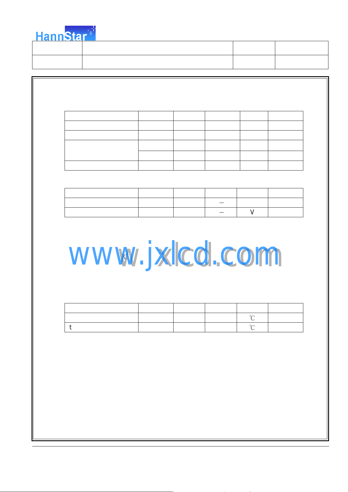
2.0 ABSOLUTE MAXIMUM RATINGS
2.1 Electrical Absolute Rating
2.1.1 TFT LCD Module
Item Symbol Min. Max. Unit Note
Digital Supply voltage
Analog Supply voltage
VCC -0.5 5 V
AVDD -0.5 13.5 V
Supply voltage
Digital input voltage
2.1.2 Back-Light Unit
Item Symbol Typ. Max. Unit Note
LED current IL 220
LED voltage VL 10.5
Note (1) Permanent damage may occur to the LCD module if beyond this specification.
Functional operation should be restricted to the conditions described under
normal operating conditions.
(2) Ta =25±2℃
www.jxlcd.com
www.jxlcd.com
(3) Test Condition: LED current 220 mA. The LED lifetime could be decreased if
operating IL is larger than 220mA.
2.2 Environment Absolute Rating
Item Symbol Min. Max. Unit Note
Operating Temperature T
Storage Temperature T
V1~V7 0.4AVDD AVDD+0.3
V8~V14 -0.3 0.6AVDD
- -0.5 VCC+0.5
-
mA (1) (2)(3)
-
V (1) (2)(3)
-20 70
opa
-30 80
stg
V
V
V
℃
℃
disclosed, distributed or reproduced in whole or in part without written permission of HannStar Display Corporation.
HannStar Display Corp.
The information contained in this document is the exclusive property of HannStar Display Corporation. It shall not be
Document Title HSD100IXN1 Formal Standard Specification Page No. 6/31
Document No. Revision 1.0
3.0 OPTICAL CHARACTERISTICS
3.1 Optical specification
Item Symbol Condition Min. Typ. Max. Unit Note
Contrast CR
Response
time
White luminance
(Center)
Color
chromaticity
(CIE1931)
Viewing
angle
Brightness uniformity B
www.jxlcd.com
Optima View Direction
3.2 Measuring Condition
www.jxlcd.com
■ Measuring surrounding:dark room
■ LED current I
■ Ambient temperature:25±2oC
■ 15min. warm-up time.
Rising TR
Falling TF
White
Hor.
Ver.
480 600
-
Θ=0
Normal
YL 200 250
Wx
Wy
Θ
Θ
Θ
Θ
UNI
:
220mA
L
L
R
U
D
viewing
angle
CR>10
Θ=0
-
0.260 0.310 0.360
0.280 0.330 0.380
65 75
65 75
50 60
60 70
70
6 O’clock
-
2.4 4.8
5.6 11.2
-
-
-
-
-
-
-
(1)(2)
msec
2
cd/m
(IL=220mA)
% (5)
(1)(3)
(1)(4)
(1)(4)
(6)
disclosed, distributed or reproduced in whole or in part without written permission of HannStar Display Corporation.
HannStar Display Corp.
The information contained in this document is the exclusive property of HannStar Display Corporation. It shall not be
o
Document Title HSD100IXN1 Formal Standard Specification Page No. 7/31
Document No. Revision 1.0
3.3 Measuring Equipment
■ FPM520 of Westar Display technologies, INC., which utilized SR-3 for Chromaticity
and BM-5A for other optical characteristics.
■ Measuring spot size:20 ~ 21 mm
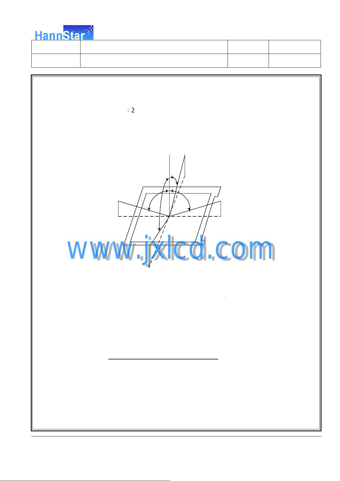
Note (1) Definition of Viewing Angle:
Note (2) Definition of Contrast Ratio (CR) :
measured at the center point of panel
Luminance with all pixels white
CR =
Luminance with all pixels black
www.jxlcd.com
www.jxlcd.com
Φ=180
Θ
L
6’ o’clock
Φ=270
Θ
D
Θ
U
12’ o’clock
Φ=90
Θ
o
o
R
Φ=0o
disclosed, distributed or reproduced in whole or in part without written permission of HannStar Display Corporation.
HannStar Display Corp.
The information contained in this document is the exclusive property of HannStar Display Corporation. It shall not be
Document Title HSD100IXN1 Formal Standard Specification Page No. 8/31
Document No. Revision 1.0
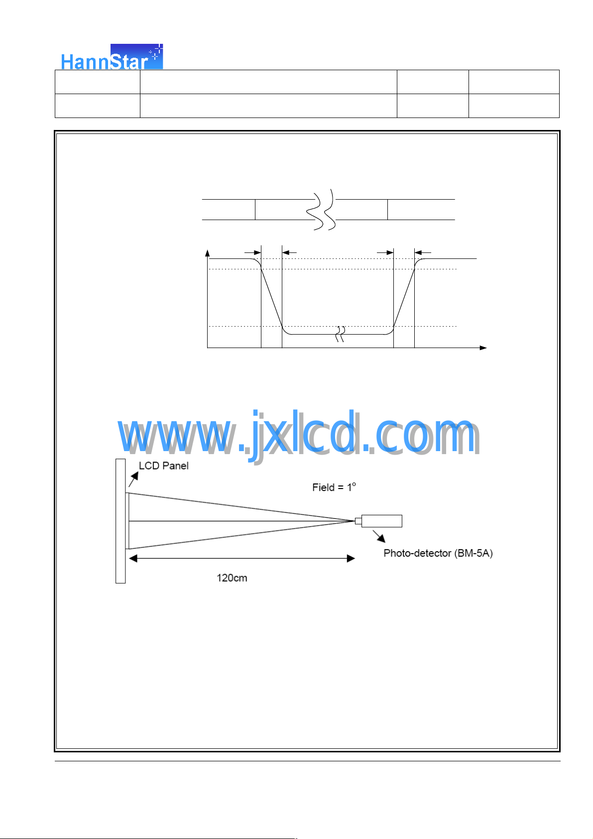
Note (3) Definition of Response Time : Sum of TR and TF
white(TFT OFF) black (TFT ON) white(TFT OFF)
T
R
100%
90%
Optical
response
Note (4) Definition of optical measurement setup
www.jxlcd.com
www.jxlcd.com
10%
0%
T
F
time
disclosed, distributed or reproduced in whole or in part without written permission of HannStar Display Corporation.
HannStar Display Corp.
The information contained in this document is the exclusive property of HannStar Display Corporation. It shall not be
Document Title HSD100IXN1 Formal Standard Specification Page No. 9/31
Document No. Revision 1.0
Note (5) Definition of brightness uniformity
16.67% 50.00% 83.33%
Y2 Y3 Y4
Y9 Y1 Y5
Y8 Y7 Y6
16.67%
50.00%
83.33%
www.jxlcd.com
www.jxlcd.com
Luminance uniformity = ×100%
Note (6):Rubbing Direction (The different Rubbing Direction will cause the different
optima view direction.
(Min Luminance of 9 points)
(Max Luminance of 9 points)
disclosed, distributed or reproduced in whole or in part without written permission of HannStar Display Corporation.
HannStar Display Corp.
The information contained in this document is the exclusive property of HannStar Display Corporation. It shall not be
1024 pixel (3072 Dots)
B G
Document Title HSD100IXN1 Formal Standard Specification Page No. 10/31
Document No. Revision 1.0
4.0 BLOCK DIAGRAM
4.1 TFT LCD Module:
1024(RGB)x768
G/D
CN3
www.jxlcd.com
www.jxlcd.com
4.2 Pixel Format
1,1
2,1
768,1
1,2 1,3 1,4
X-PCB
S/D S/D
LED
CN2
S/D
CN1
1,1024
LCD Display Area
1 Pixel
R
R
R
768,
1024
768 Lines
disclosed, distributed or reproduced in whole or in part without written permission of HannStar Display Corporation.

HannStar Display Corp.
The information contained in this document is the exclusive property of HannStar Display Corporation. It shall not be
Vertical Line start pulse I/O signal
Vertical Line
Vertical Line Clock
Vertical Line start pulse I/O signal
Document Title HSD100IXN1 Formal Standard Specification Page No. 11/31
Document No. Revision 1.0
5.0 INTERFACE PIN CONNECTION
5.1 TFT LCD Module
CN1 (Input signal): 30pin, 0.5mm pitch, 196033-30041-3 (P-TWO or equivalent)
Pin No. Signal Description
1 POL Polarity Setting
2 STVD
3 OE123R
4 G-CLKR
5 STVU
6 GND Digital Power Ground
7 EDGSEL
8 VCC Digital Voltage Input
9 V9 Gamma Voltage Input
10 VGL Gate OFF Voltage
11 V2 Gamma Voltage Input
12 VGH Gate ON Voltage
13 V6 Gamma Voltage Input
14 UDC
www.jxlcd.com
www.jxlcd.com
15 VCOM Common Voltage
16 AGND Analog Power Ground
17 AVDD Analog Voltage Input
18 V14 Gamma Voltage Input
19 V11 Gamma Voltage Input
20 V8 Gamma Voltage Input
21 V5 Gamma Voltage Input
22 V3 Gamma Voltage Input
23 GND Digital Power Ground
24 R5 Red Data Bus Input (MSB)
25 R4 Red Data Bus Input
26 R3 Red Data Bus Input
27 R2 Red Data Bus Input
28 R1 Red Data Bus Input
29 R0 Red Data Bus Input (LSB)
30 GND Digital Power Ground
:
:
::
output Enable signal
Define clock edge select input, default EDGSEL=L.
EDGSEL=L Latch data by rising edge of clock
EDGSEL=H Latch data by rising and falling edges of clock
Shift up/down control signal
UDC = "H", up shift:
STVD (Input) G1 ~ G600STVU (Output)
UDC= "L", down shift:
STVU (Input) G600~G1STVD (Output)
disclosed, distributed or reproduced in whole or in part without written permission of HannStar Display Corporation.

HannStar Display Corp.
The information contained in this document is the exclusive property of HannStar Display Corporation. It shall not be
Document Title HSD100IXN1 Formal Standard Specification Page No. 12/31
Document No. Revision 1.0
CN2 (Input signal): 30pin, 0.5mm pitch,196033-30041-3 (P-TWO or equivalent)
Pin No. Signal Description
1 GND Digital Power Ground
2 G5 Green Data Bus Input (MSB)
3 G4 Green Data Bus Input
4 G3 Green Data Bus Input
5 G2 Green Data Bus Input
6 G1 Green Data Bus Input
7 G0 Green Data Bus Input (LSB)
8 DIO2_COF3 Horizontal Line start pulse I/O signal (STHR)
9 REV Data Invert signal
10 GND Digital Power Ground
11 CLK Pixel clock
12 VCC Digital Voltage Input
13 DIO1_COF1 Horizontal Line start pulse I/O signal (STHL)
14 LD Polarity latch and re-flash new data to output
15 B5 Blue Data Bus Input (MSB)
16 B4 Blue Data Bus Input
17 B3 Blue Data Bus Input
18 B2 Blue Data Bus Input
19 B1 Blue Data Bus Input
20 B0 Blue Data Bus Input (LSB)
Select left or right shift, normally pulled high.
www.jxlcd.com
21 LRC
www.jxlcd.com
22 V1 Gamma Voltage Input
23 V4 Gamma Voltage Input
24 V7 Gamma Voltage Input
25 V10 Gamma Voltage Input
26 V12 Gamma Voltage Input
27 V13 Gamma Voltage Input
28 AVDD Analog Voltage Input
29 AGND Analog Power Ground
30 VCOM Common Voltage
5.2 Back-Light Unit
CN3 LED Power Source (BHSR-02VS-1) or equivalent
Mating Connector: (SBHT-002T-P0.5) or equivalent
Terminal no. Symbol Function
1 VL LED power supply (high voltage)
2 GL LED power supply (low voltage)
SHL=“1”: DIO1 OUT1,2,3OUT4,5,6
OUT1198,1199,1200 = DIO2
SHL=“0”: DIO1= OUT1,2,3 OUT4,5,6
OUT1198,1199,1200DIO2
disclosed, distributed or reproduced in whole or in part without written permission of HannStar Display Corporation.

HannStar Display Corp.
The information contained in this document is the exclusive property of HannStar Display Corporation. It shall not be
ent of power
Document Title HSD100IXN1 Formal Standard Specification Page No. 13/31
Document No. Revision 1.0
6.0 ELECTRICAL CHARACTERISTICS
6.1 TFT LCD Module
Item Symbol Min. Typ. Max. Unit
Vcc 3.0 3.3 3.6 V Note (2), Note (3)
Supply Voltage
VGH 16.55 17 17.45 V Note (2), Note (3)
VGL -7.35 -7 -6.65 V Note (2), Note (3)
AVDD 9.22 9.48 9.75 V Note (2), Note (3)
Note
VCOM V
Input signal
voltage
Curr
supply
Input level of
V1~V5
Input level of
V6~V10
www.jxlcd.com
Note (1): HSYNC, VSYNC, DE, Digital Data
Note (2): Be sure to apply the power voltage as the power sequence spec.
Note (3): DGND=AGND=0V
www.jxlcd.com
COMin
- 3.19
ViH 0.7 Vcc
ViL 0 - 0.3 Vcc
ICC - 8.3 - mA Vcc = 3.3V (Black)
I
ADD
- 70 - mA AVDD= 9.5 V (Black)
IGH - 0.3 - mA VGH= 17 V
IGL - 0.6 - mA VGL= -7 V
Vx AVDD/2
Vx 0.1 - AVDD/2
- Vcc V Note (1)
- AVDD-0.1
- V
V
V
V
disclosed, distributed or reproduced in whole or in part without written permission of HannStar Display Corporation.

HannStar Display Corp.
The information contained in this document is the exclusive property of HannStar Display Corporation. It shall not be
White (
Ground)
Black
2
Document Title HSD100IXN1 Formal Standard Specification Page No. 14/31
Document No. Revision 1.0
6.2 Back-Light Unit
The back-light system is an edge-lighting type with 33 LED.
The characteristics of the LED are shown in the following tables.
Item Symbol Min. Typ. Max.
LED current IL
LED voltage VL
Operating LED life time
Hr 20000
-
220
-
10.5
-
-
-
-
mA (2)
V
Hour (1)(2)
Unit Note
LCD MODULE
1
Power Supply
A
Note (1) LED life time (Hr) can be defined as the time in which it continues to
www.jxlcd.com
www.jxlcd.com
Note (2) The “LED life time” is defined as the module brightness decrease to
operate under the condition: Ta=25±3 oC, typical IL value indicated in
the above table until the brightness becomes less than 50%.
50% original brightness at Ta=25℃ and IL=220mA. The LED lifetime
could be decreased if operating IL is larger than 220mA. The
constant current driving method is suggested.
LED Light Bar Circuit
disclosed, distributed or reproduced in whole or in part without written permission of HannStar Display Corporation.

HannStar Display Corp.
The information contained in this document is the exclusive property of HannStar Display Corporation. It shall not be
Document Title HSD100IXN1 Formal Standard Specification Page No. 15/31
Document No. Revision 1.0
Note (3) Suggested Schematic of LED Back-Light Driver
www.jxlcd.com
www.jxlcd.com
Suggested Schematic of LED Back-Light Driver
disclosed, distributed or reproduced in whole or in part without written permission of HannStar Display Corporation.

HannStar Display Corp.
The information contained in this document is the exclusive property of HannStar Display Corporation. It shall not be
Document Title HSD100IXN1 Formal Standard Specification Page No. 16/31
Document No. Revision 1.0
6.3 AC Characteristics
Source Driver Timing
Item Symbol Min. Typ. Max.
CLK frequency Fclk - 56 60 MHz CLK pulse width Tcw
Data set-up time Tsu
Data hold time Thd
Propagation delay of DIO2/1 Tphl
Time that the last data to LD Tld
Pulse width of LD Twld
Time that LD to DIO1/2 Tlds
POL set-up time Tpsu
POL hold time
Tphd
6 4 2 -
6 10 15
1 -
2 - 5 - 6 - 6
- ns -
- ns -
- ns -
- Tcph -
ns
Unit Note
ns
Tcph Tcph -
ns
CL=25pF
( Output )
POL to LD
POL to LD
Gate Driver Timing
Item Symbol Min. Typ. Max.
CPV period Tcpv
www.jxlcd.com
www.jxlcd.com
CPV pulse width
OE pulse width Twoe
Data setup time Tsu
Data hold time Thd
Tcpvh,
Tcpvl
5
2.5 - 1 - -
200
300
- - us -
- -
- -
Unit Note
us 50% duty cycle
us -
ns ns -
disclosed, distributed or reproduced in whole or in part without written permission of HannStar Display Corporation.

HannStar Display Corp.
The information contained in this document is the exclusive property of HannStar Display Corporation. It shall not be
Document Title HSD100IXN1 Formal Standard Specification Page No. 17/31
Document No. Revision 1.0
6.4 Timing Diagram of Interface Signal
Source Driver Timing
Tcph
70% 70%
30%
Tcw
CLK
DIO1/2
70%
70%
Tsu
Thd
70%
70%
30%
Tcw
70%
(input)
Tsu
Thd
Data,REV
70%
First data Second data Last data
Tphl
DIO1/2
(output)
www.jxlcd.com
www.jxlcd.com
CLK
70%
70%
Tld
70% 70%
LD
Twld
Tlds
DIO1/2
(input)
70%
70%
Tphl
30%
70%
LD
Tpsu Tphd
POL
70%
70%
disclosed, distributed or reproduced in whole or in part without written permission of HannStar Display Corporation.

HannStar Display Corp.
The information contained in this document is the exclusive property of HannStar Display Corporation. It shall not be
Document Title HSD100IXN1 Formal Standard Specification Page No. 18/31
Document No. Revision 1.0
Gate Driver Timing
Tcph Tcpl
Tcpv
50%
CPV
Tsu
STVU
Twoe
50%
OE
www.jxlcd.com
www.jxlcd.com
Thd
50%
disclosed, distributed or reproduced in whole or in part without written permission of HannStar Display Corporation.

HannStar Display Corp.
The information contained in this document is the exclusive property of HannStar Display Corporation. It shall not be
0.9VDD
0.9VDD
Document Title HSD100IXN1 Formal Standard Specification Page No. 19/31
Document No. Revision 1.0
6.5 Power On / Off Sequence
Power On
Power Off
Power Supply
0V
0V
0.1V
Signal
DD
TP1
TP2
0.6V
TP5
TP3
0.6V
TP6
0.1V
DD
TP4
0.1V
DD
Backlight
(Recommended)
www.jxlcd.com
www.jxlcd.com
Item Min. Typ. Max. Unit Remark
TP1 0.5 -- 10 msec
TP2 0 -- 50 msec
TP3 0 -- 50 msec
TP4 500 -- -- msec
TP5 200 -- -- msec
TP6 200 -- -- msec
50%
50%
Level define
90%
10%
T
Power On Sequence: VCC-> AVDD -> VGL -> VGH -> Data -> B/L
Power Off Sequence: B/L-> Data -> VGH -> VGL -> AVDD -> VCC
Notes: Data include R0~R7, G0~G7, B0~B7, HSD, VSD, DCLK, SHLR, UPDN, DE
MODE, RSTB, STBYB, SHLR, UPDN, DITH
disclosed, distributed or reproduced in whole or in part without written permission of HannStar Display Corporation.

HannStar Display Corp.
The information contained in this document is the exclusive property of HannStar Display Corporation. It shall not be
Document Title HSD100IXN1 Formal Standard Specification Page No. 20/31
Document No. Revision 1.0
6.6 Gamma circuit
www.jxlcd.com
www.jxlcd.com
*Suggested Gamma Circuit(AVDD=9.5V).
disclosed, distributed or reproduced in whole or in part without written permission of HannStar Display Corporation.

HannStar Display Corp.
The information contained in this document is the exclusive property of HannStar Display Corporation. It shall not be
C(30min), 200cycles
Document Title HSD100IXN1 Formal Standard Specification Page No. 21/31
Document No. Revision 1.0
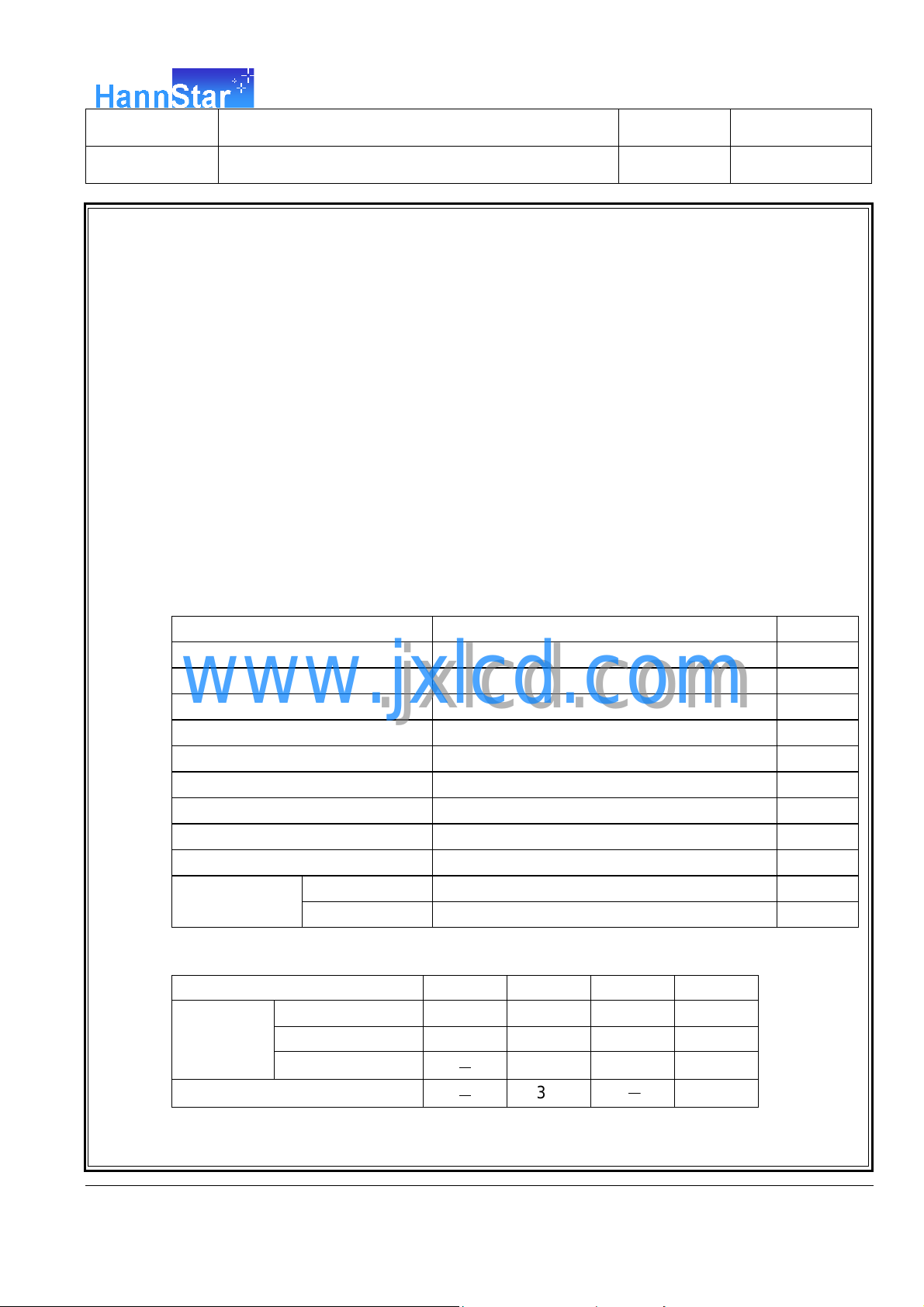
7.0 Reliability test items
No. Item Conditions Remark
1 High Temperature Storage Ta=+80oC, 240hrs
2 Low Temperature Storage Ta=-30oC, 240hrs
High Temperature Operation Ta=+70oC, 240hrs
3
Low Temperature Operation Ta=-20oC, 240hrs
4
5 High Temperature and High Humidity
(operation)
6 Thermal Cycling Test (non operation) -30oC(30min) → +80
7 Electrostatic Discharge
8 Vibration
9 Shock
www.jxlcd.com
10 Vibration (with carton)
11 Drop (with carton)
Note: There is no display function NG issue occurred, all the cosmetic specification is judged
www.jxlcd.com
before the reliability stress.
1.Random:
2. Sine:
100G, 6ms, ±X, ±Y, ±Z
3 time for each direction
Random: 0.015G^2/Hz, 5~200Hz
-6dB/Octave, 200~400Hz
XYZ each direction: 2hr
Height: 60cm
1 corner, 3 edges, 6 surfaces
Ta=+60oC, 90%RH, 240hrs
o
±
200V,200pF(0Ω) 1 time/each terminal
1.04Grms, 5~500Hz, X/Y/Z,
30min/each direction
Freq. Range: 8~33.3Hz
Stoke: 1.3mm
Sweep: 2.9G, 33.3~400Hz
X/Z: 2hr, Y: 4hr, cyc: 15min
JIS C7021, A-10
(Condition A)
JIS Z0202
disclosed, distributed or reproduced in whole or in part without written permission of HannStar Display Corporation.

HannStar Display Corp.
The information contained in this document is the exclusive property of HannStar Display Corporation. It shall not be
Document Title HSD100IXN1 Formal Standard Specification Page No. 22/31
Document No. Revision 1.0
8.0 OUTLINE DIMENSION
8.1 Outline Dimension
Note : General Tolerance : +/- 0.3mm
www.jxlcd.com
www.jxlcd.com
nit : mm
disclosed, distributed or reproduced in whole or in part without written permission of HannStar Display Corporation.

HannStar Display Corp.
The information contained in this document is the exclusive property of HannStar Display Corporation. It shall not be
2
3
4
5
6
7
8
9
10
11
12
13
14
15
Rev
: -
A**
6 A0
Document Title HSD100IXN1 Formal Standard Specification Page No. 23/31
Document No. Revision 1.0
9.0 LOT MARK
9.1 Lot Mark
1
Code 1,2,3,4,5,6: HannStar internal flow control code.
Code 7: production location.
Code 8: production year.
Code 9: production month.
Code 10,11,12,13,14,15: serial number.
Note (1) Production Year: Code 8 is defined by the last number of the year, for example
Year 2006 2007 2008 2009 2010 2011 2012 2013 2014 2015
Mark 6 7 8 9 0 1 2 3 4 5
Note (2) Production Month
Month Jan. Feb. Mar. Apr. May. Jun. Jul. Aug. Sep. Oct Nov. Dec.
Mark 1 2 3 4 5 6 7 8 9 A B C
www.jxlcd.com
9.2
www.jxlcd.com
Detail of Lot Mark
(1) Below label is attached on the backside of the LCD module. See Section 8.0: Outline
Dimension.
(2) The detail of Lot Mark is attached as below.
(3) This is subject to change without prior notice.
GP-HF
HSD100IXN1
HannStar
disclosed, distributed or reproduced in whole or in part without written permission of HannStar Display Corporation.

HannStar Display Corp.
The information contained in this document is the exclusive property of HannStar Display Corporation. It shall not be
Document Title HSD100IXN1 Formal Standard Specification Page No. 24/31
Document No. Revision 1.0
10.0 PACKAGE SPECIFICATION
10.1 Packing form
LCM Model LCM Qty. in the box
HSD100IXN1-A
10.2 Packing assembly drawings
Inner Box Size
60 pcs/box
www.jxlcd.com
www.jxlcd.com
Ref.538 x 302 x 417
(mm)
H
Notice
Material Notice
Box Corrugated Paper Board
Partition/Pad Corrugated Paper Board
Corner Pad Corrugated Paper Board
ESD bag PE
disclosed, distributed or reproduced in whole or in part without written permission of HannStar Display Corporation.
(AB Flute)
(B Flute)
(AB Flute)

HannStar Display Corp.
The information contained in this document is the exclusive property of HannStar Display Corporation. It shall not be
Document Title HSD100IXN1 Formal Standard Specification Page No. 25/31
Document No. Revision 1.0
11.0 GENERAL PRECAUTION
11.1 Use Restriction
This product is not authorized for use in life supporting systems, aircraft navigation control
systems, military systems and any other application where performance failure could be
life-threatening or otherwise catastrophic.
11.2 Disassembling or Modification
Do not disassemble or modify the module. It may damage sensitive parts inside LCD
module, and may cause scratches or dust on the display. HannStar does not warrant the
module, if customers disassemble or modify the module.
11.3 Breakage of LCD Panel
11.3.1.If LCD panel is broken and liquid crystal spills out, do not ingest or inhale liquid
crystal, and do not contact liquid crystal with skin.
11.3.2. If liquid crystal contacts mouth or eyes, rinse out with water immediately.
11.3.3. If liquid crystal contacts skin or cloths, wash it off immediately with alcohol and
rinse thoroughly with water.
11.3.4. Handle carefully with chips of glass that may cause injury, when the glass is
broken.
11.4 Electric Shock
www.jxlcd.com
www.jxlcd.com
11.4.1. Disconnect power supply before handling LCD module.
11.4.2. Do not pull or fold the LED cable.
11.4.3. Do not touch the parts inside LCD modules and the fluorescent LED’s connector
or cables in order to prevent electric shock.
11.5 Absolute Maximum Ratings and Power Protection Circuit
11.5.1. Do not exceed the absolute maximum rating values, such as the supply voltage
variation, input voltage variation, variation in parts’ parameters, environmental
temperature, etc., otherwise LCD module may be damaged.
11.5.2. Please do not leave LCD module in the environment of high humidity and high
temperature for a long time.
11.5.3. It’s recommended to employ protection circuit for power supply.
11.6 Operation
11.6.1 Do not touch, push or rub the polarizer with anything harder than HB pencil lead.
11.6.2 Use fingerstalls of soft gloves in order to keep clean display quality, when persons
handle the LCD module for incoming inspection or assembly.
11.6.3 When the surface is dusty, please wipe gently with absorbent cotton or other soft
material.
disclosed, distributed or reproduced in whole or in part without written permission of HannStar Display Corporation.

HannStar Display Corp.
The information contained in this document is the exclusive property of HannStar Display Corporation. It shall not be
Document Title HSD100IXN1 Formal Standard Specification Page No. 26/31
Document No. Revision 1.0
11.6.4 Wipe off saliva or water drops as soon as possible. If saliva or water drops
contact with polarizer for a long time, they may causes deformation or color
fading.
11.6.5 When cleaning the adhesives, please use absorbent cotton wetted with a little
petroleum benzine or other adequate solvent.
11.7 Mechanism
Please mount LCD module by using mounting holes arranged in four corners tightly.
11.8 Static Electricity
11.8.1 Protection film must remove very slowly from the surface of LCD module to
prevent from electrostatic occurrence.
11.8.2 Because LCD module use CMOS-IC on circuit board and TFT-LCD panel, it is
very weak to electrostatic discharge. Please be careful with electrostatic
discharge. Persons who handle the module should be grounded through
adequate methods.
11.9 Strong Light Exposure
The module shall not be exposed under strong light such as direct sunlight. Otherwise,
display characteristics may be changed.
www.jxlcd.com
11.10 Disposal
When disposing LCD module, obey the local environmental regulations.
www.jxlcd.com
disclosed, distributed or reproduced in whole or in part without written permission of HannStar Display Corporation.

HannStar Display Corp.
The information contained in this document is the exclusive property of HannStar Display Corporation. It shall not be
Document Title HSD100IXN1 Formal Standard Specification Page No. 27/31
Document No. Revision 1.0
HSD100IXN1-A10
3.1 Optical specification
Item Symbol Condition Min. Typ. Max. Unit Note
Contrast CR
Response
time
White luminance
(Center)
Color gamut S
Color
chromaticity
(CIE1931)
www.jxlcd.com
www.jxlcd.com
Viewing
angle
Rising TR
Falling TF
YL 200 250
Wx
White
Wy
Rx
Red
Ry
Gx
Green
Gy
Bx
Blue
By
Θ
Hor.
Θ
Θ
Ver.
Θ
L
R
U
D
CR>10
Θ=0
Normal
viewing
angle
480 600
-
-
-
0.280 0.310 0.340
0.300 0.330 0.360
0.579
0.326
0.289
0.557
0.124
0.056
65 75
65 75
50 60
60 70
2.4 4.8
5.6 11.2
60
0.609
0.356
0.319
0.587
0.154
0.086
-
-
-
0.639
0.386
0.349
0.617
0.184
0.116
-
-
-
-
(1)(2)
msec
2
cd/m
%
(IL=120mA)
(1)(3)
(1)(4)
(1)(4)
Brightness uniformity B
Optima View Direction
disclosed, distributed or reproduced in whole or in part without written permission of HannStar Display Corporation.
UNI
Θ=0
70
6 O’clock
- -
% (5)
(6)

HannStar Display Corp.
The information contained in this document is the exclusive property of HannStar Display Corporation. It shall not be
Vertical Line start pulse I/O signal
Vertical Line output Enable signal
Vertical Line Clock
Vertical Line start pulse I/O signal
Document Title HSD100IXN1 Formal Standard Specification Page No. 28/31
Document No. Revision 1.0
5.3 TFT LCD Module
CN (Input signal): 60pin, 0.5mm pitch, 106C60-102000-G2-R (Starconn or equivalent)
Pin No. Signal Description
1 POL Polarity Setting
2 STVD
3 OE123R
4 G-CLKR
5 STVU
6 GND Digital Power Ground
7 EDGSEL
8 VCC Digital Voltage Input
9 V9 Gamma Voltage Input
10 VGL Gate OFF Voltage
11 V2 Gamma Voltage Input
12 VGH Gate ON Voltage
13 V6 Gamma Voltage Input
14 UDC
www.jxlcd.com
www.jxlcd.com
15 VCOM Common Voltage
16 AGND Analog Power Ground
17 AVDD Analog Voltage Input
18 V14 Gamma Voltage Input
19 V11 Gamma Voltage Input
20 V8 Gamma Voltage Input
21 V5 Gamma Voltage Input
22 V3 Gamma Voltage Input
23 GND Digital Power Ground
24 R5 Red Data Bus Input (MSB)
25 R4 Red Data Bus Input
26 R3 Red Data Bus Input
27 R2 Red Data Bus Input
28 R1 Red Data Bus Input
29 R0 Red Data Bus Input (LSB)
30 GND Digital Power Ground
:
:
::
Define clock edge select input, default EDGSEL=L.
EDGSEL=L Latch data by rising edge of clock
EDGSEL=H Latch data by rising and falling edges of clock
Shift up/down control signal
UDC = "H", up shift:
STVD (Input) G1 ~ G600STVU (Output)
UDC= "L", down shift:
STVU (Input) G600~G1STVD (Output)
disclosed, distributed or reproduced in whole or in part without written permission of HannStar Display Corporation.

HannStar Display Corp.
The information contained in this document is the exclusive property of HannStar Display Corporation. It shall not be
Document Title HSD100IXN1 Formal Standard Specification Page No. 29/31
Document No. Revision 1.0
Pin No. Signal Description
31 GND Digital Power Ground
32 G5 Green Data Bus Input (MSB)
33 G4 Green Data Bus Input
34 G3 Green Data Bus Input
35 G2 Green Data Bus Input
36 G1 Green Data Bus Input
37 G0 Green Data Bus Input (LSB)
38 DIO2_COF3 Horizontal Line start pulse I/O signal (STHR)
39 REV Data Invert signal
40 GND Digital Power Ground
41 CLK Pixel clock
42 VCC Digital Voltage Input
43 DIO1_COF1 Horizontal Line start pulse I/O signal (STHL)
44 LD Polarity latch and re-flash new data to output
45 B5 Blue Data Bus Input (MSB)
46 B4 Blue Data Bus Input
47 B3 Blue Data Bus Input
48 B2 Blue Data Bus Input
49 B1 Blue Data Bus Input
50 B0 Blue Data Bus Input (LSB)
Select left or right shift, normally pulled high.
www.jxlcd.com
51 LRC
www.jxlcd.com
52 V1 Gamma Voltage Input
53 V4 Gamma Voltage Input
54 V7 Gamma Voltage Input
55 V10 Gamma Voltage Input
56 V12 Gamma Voltage Input
57 V13 Gamma Voltage Input
58 AVDD Analog Voltage Input
59 AGND Analog Power Ground
60 VCOM Common Voltage
6.6 Back-Light Unit
The back-light system is an edge-lighting type with 33 LED.
The characteristics of the LED are shown in the following tables.
Item Symbol Min. Typ. Max.
LED current IL
LED voltage VL
Operating LED life time
SHL=“1”: DIO1 OUT1,2,3OUT4,5,6
OUT1198,1199,1200 = DIO2
SHL=“0”: DIO1= OUT1,2,3 OUT4,5,6
OUT1198,1199,1200DIO2
-
220
-
10.5
Hr 20000
-
-
mA (2)
11 V
-
Hour (1)(2)
Unit Note
disclosed, distributed or reproduced in whole or in part without written permission of HannStar Display Corporation.

HannStar Display Corp.
The information contained in this document is the exclusive property of HannStar Display Corporation. It shall not be
Document Title HSD100IXN1 Formal Standard Specification Page No. 30/31
Document No. Revision 1.0
Source Driver Timing
Item Symbol Min. Typ. Max.
CLK frequency Fclk 48 56 60 MHz
CLK pulse width Tcw
Data set-up time Tsu
Data hold time Thd
Propagation delay of DIO2/1 Tphl
Time that the last data to LD Tld
Pulse width of LD Twld
Time that LD to DIO1/2 Tlds
POL set-up time Tpsu
POL hold time
Tphd
6 4 2 -
6 10 15
1 -
2 - 5 - 6 - 6
- ns -
- ns -
- ns -
- Tcph -
ns
Unit Note
Frame rate at
60Hz
ns
Tcph Tcph -
ns
CL=25pF
( Output )
POL to LD
POL to LD
Gate Driver Timing
Item Symbol Min. Typ. Max.
CPV period Tcpv
www.jxlcd.com
www.jxlcd.com
CPV pulse width
OE pulse width Twoe
Data setup time Tsu
Data hold time Thd
Tcpvh,
Tcpvl
5
2.5 - 1 - -
200
300
- - us -
- -
- -
Unit Note
us 50% duty cycle
us -
ns ns -
disclosed, distributed or reproduced in whole or in part without written permission of HannStar Display Corporation.

HannStar Display Corp.
The information contained in this document is the exclusive property of HannStar Display Corporation. It shall not be
Document Title HSD100IXN1 Formal Standard Specification Page No. 31/31
Document No. Revision 1.0
8.1 Outline Dimension
www.jxlcd.com
www.jxlcd.com
disclosed, distributed or reproduced in whole or in part without written permission of HannStar Display Corporation.
 Loading...