Hangzhou Tuya Information Technology WRG1 User Manual

WRG1 User Manual
1. Product Overview
WRG1 is a low power-consuming built-in Wi-Fi module developed by Hangzhou Tuya
Information Technology Co., Ltd. It consists of a highly integrated radio frequency chip
(RTL8711AM) and an external flash chip, with a built-in Wi-Fi network protocol stack and robust
library functions. WRG1 also contains a low power-consuming ARM-Cortex M3 MCU, a
WLAN MAC, a 1T1R WLAN, and the maximum basic frequency of 166 MHz, and is embedded
with a 2MB SDRAM ,4Mbyte flash, and robust peripheral resources.
WRG1 is an RTOS platform that integrates all the function libraries of the Wi-Fi MAC
and TCP/IP protocols. You can develop built-in Wi-Fi products as required.
1.1 Features
Built-in low power-consuming 32-bit CPU functioning as an application processor
Basic frequency: 166 MHz
Working voltage: 3 V to 3.6 V
Peripherals: ten GPIOs, two UARTs, and one ADC
Wi-Fi connectivity
802.11 B/G/N20/N40
Channels 1-11@2.4GHz
Supports WPA/WPA2 safe modes
SmartConfig mode (for Android and iOS devices)
Passing the CE, FCC, and SRRC certification
Working temperature: –20°C to +85°C
1.2 Major Application Fields
Intelligent building
Intelligent home and household appliances
Healthcare
Industrial wireless control
Baby monitors
Network camera
Intelligent bus
Version1.0.2

WRG1 User Manual
2. Module Interfaces
2.1 Dimensions and Pin Layout
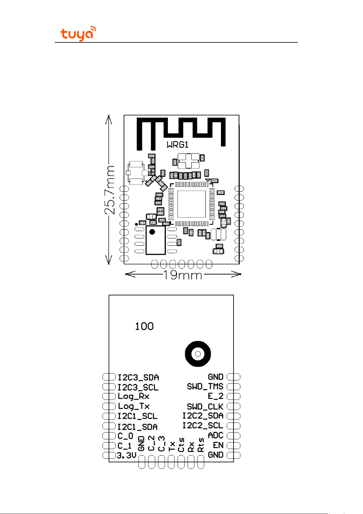
WRG1 provides three rows of pins with the distance of 1.5 mm between every two pins.
WRG1 dimensions: 19±0.25 mm (W) x 25.7±0.25 mm (L) x 3.6±0.2 mm (H)
Version1.0.2

2.2 Pin definition
Table 2.1 describes the common pins.
Table 2.1,WRG1 pins description
No. Symbol I/OType Function
1 GND P
2 SWD_TMS AI
3 E_2 I
4 SWD_CLK I/O
5 I2C2_SDA I/O
6 I2C2_SCL I/O
7 ADC AI ADC
8 EN P
9 GND P
10 Rts I/O
Power Reference Ground
GPIOE_3,JTAG_TMS,used as JLink Burning foot
GPIOE_2,if E3/E4 configured to JTAG,the
foot is not configurable to GPIO。
GPIOE_4,JTAG_CLK,used as JLink Burning foot
GPIOE_1,if E3/E4 configured to JTAG,the
foot is not configurable to GPIO。
GPIOE_0,if E3/E4 configured to JTAG,the
foot is not configurable to GPIO。
(1)
port
,16-bit accuracy ADC
Module enabling foot, normal use needs to be
connected to 3.3V, module has been pulled up
Power Reference Ground
GPIOA_3, Flow control send request foot, if A6/A7 is configured
as UART0,the foot is not configurable to GPIO。
WRG1
User Manual
11 Rx I/O
12 Cts I/O
13 Tx I/O
14 C_3 I/O
15 C_2 I/O
16 GND P
17 3.3V P
18 C_1 I/O
19 C_0 I/O
20 I2C1_SDA I/O
21 I2C1_SCL I/O
22 Log_Tx I/O
23 Log_Rx I/O
24 I2C3_SCL I/O
25 I2C3_SDA I/O
GPIOA_6,UART0_Rx,User docking serial port
GPIOA_5, Flow control sending allowable foot,if A6/A7
configured to UART0,he foot is not configurable to GPIO。
GPIOA_7,UART0_Tx,User docking serial port
GPIOC_3,hardware PWM3
GPIOC_2,hardware PWM2
Power Reference Ground
Power pin of module(3.3V)
GPIOC_1,hardware PWM1
GPIOC_0,hardware PWM0
GPIOC_4,the foot is not configurable to I2C or GPIO
GPIOC_5, can be configurable to I2C or GPIO
GPIOB_0,Log Tx,Serial port print information
pin, can not
GPIOB_1,Log Rx,Serial port printing information pin
connect high level
GPIOB_2,can be configurable to I2C or GPIO
GPIOB_3,can be configurable to I2C or GPIO
Note: P indicates power-supply pins, I/O indicates input/output pins
(1)The pin can only be used as ADC port, not ordinary IO port. When not in use, it needs to
be suspended.
As the input port of ADC, the range of input voltage is limited to 0-3.3V.
(2)UART0 is the user serial port. When the module is powered on and started, the serial
port has information output, which can be ignored by the user.

3. Electrical Parameters
3.1 Absolute electrical parameters
Table 3.1,Absolute Parameters
WRG1
User Manual
Parameters Description
Ts
VDD
Static electricity voltage
(human model)
Static electricity voltage
(machine model)
3.2 Electrical Conditions
Table 3.2 Normal electrical conditions
Paramet
ers
Ta
Description Min Typ Max Unit
Working
temperature
Minimu
m value
Storage
temperature
Power-supply
voltage
TAMB –
25°C
TAMB –
25°C
–20 - 85 °C
–40 105 °C
–0.3 3.6 V
- 2 kV
- 0.5 kV
Maximu
m value
Unit
VDD Working voltage 3.0 3.3 3.6 V
VIL I/O low-level input – - V
VIH I/O high-level input -
VOL I/O low-level output -
high-level
VOH
Imax I/O drive current - - 16 mA
Cpad
I/O
output
Input pin
capacitance
2.0
-
2.4
- 2 - pF
-
0.8
0.4
-
-
V
V
V
Version1.0.2
 Loading...