


TYWRD3S Datasheet
Hangzhou Tuya Information Technology Co., Ltd. 1 V2.0.2
1. Product Overview
TYWRD3S is a low-power built-in Wi-Fi module that Hangzhou Tuya Inc has developed. It
consists of a highly integrated RF chip (RDA5981B) and several peripheral components, with a
built-in Wi-Fi network protocol stack and robust library functions. TYWRD3S is embedded with a
low-power ARM-CM4 MCU, 2 MB flash memory, 448 KB SRAM, and rich peripheral resources.
TYWRD3S is an RTOS platform that integrates all the function libraries of the Wi-Fi MAC and
TCP/IP protocols. You can develop built-in Wi-Fi products as required.
1.1 Features
Built-in low-power CPU, which can also be used as an application processor
⚫ Dominant frequency: up to 160 MHz
Working voltage: 3.0 V to 3.6 V
Peripherals: nine GPIOs, one UART, and one ADC
Wi-Fi connectivity
⚫ 802.11b/g/n/HT20
⚫ 2.4GHz WIFI
⚫ WPA, WPA2, WEP, and TKIP security modes
⚫ Up to +20 dBm EIRP output power
⚫ STA, AP, and STA+AP working modes
⚫ Smart and AP network configuration modes (for Android and iOS devices)
Tuya TYWRD3S Wi-Fi Module
Version: 2.0.2
Date: 2019-11-5
Product
Manual
Global Intelligent Platform

TYWRD3S Datasheet
Hangzhou Tuya Information Technology Co., Ltd. 2 V2.0.2
⚫ Onboard PCB antenna
⚫ Working temperature: –20°C to 85C
1.2 Applications
Intelligent building
Smart household and home appliances
Smart socket and light
Industrial wireless control
Baby monitor
Network camera
Intelligent bus
Change History
No.
Date
Change Description
Version After Change
1
2019-07-26
This is the first release.
2.0.0
2
2019-07-26
Modify the pin number.
2.0.1
3
2019-07-26
Delete the Block diagram
2.0.2

TYWRD3S Datasheet
Hangzhou Tuya Information Technology Co., Ltd. 3 V2.0.2
Contents
1. Product Overview ............................................................................................................ 1
1.1 Features.................................................................................................................. 1
1.2 Applications ............................................................................................................ 2
2 Module Interfaces ............................................................................................................. 5
2.1 Dimensions and Footprint ...................................................................................... 5
2.2 Pin Definition .......................................................................................................... 5
2.3 Test Pin Definition ................................................................................................... 7
3 Electrical Parameters ........................................................................................................ 7
3.1 Absolute Electrical Parameters .............................................................................. 7
3.2 Electrical Conditions ............................................................................................... 8
3.3 Wi-Fi RX Power Consumption ............................................................................... 9
3.4 Power Consumption in Working Mode ................................................................... 9
Note: ALL the parameter vary according to the different firmware ............................................. 9
4 RF Features ...................................................................................................................... 9
4.1 Basic RF Features .................................................................................................. 9
4.2 Wi-Fi Output Power .............................................................................................. 10
4.3 Wi-Fi RX Sensitivity .............................................................................................. 10
5 Antenna Information ........................................................................................................ 11
5.1 Antenna Type .......................................................................................................... 11
5.2 Antenna Interference Reduction ................................................................................ 11
5.3 Antenna Connector Specifications ....................................................................... 11
6. Packaging Information and Production Instructions ...................................................... 12
6.1 Mechanical Dimensions ........................................................................................... 12
6.2 Recommended PCB Encapsulation ..................................................................... 13
6.3 Production Instructions ......................................................................................... 14

TYWRD3S Datasheet
Hangzhou Tuya Information Technology Co., Ltd. 4 V2.0.2
6.4 Recommended Oven Temperature Curve ........................................................... 15
6.5 Storage Conditions ............................................................................................... 16
7 MDQ and Packing Information ....................................................................................... 17
8 Appendix: Statement ....................................................................................................... 18
Figures
Figure 1 TYWRD3S front and back views ........................................................................... 5
Figure 2 TYWRD3S mechanical dimensions .................................................................... 12
Figure 3 Side view ............................................................................................................. 12
Figure 4 TYWRD3S schematic diagram and pin connection ............................................ 13
Figure 5 TYWRD3S-PCB encapsulation ............................ Error! Bookmark not defined.
Figure 6 Oven temperature curve ...................................................................................... 16
Tables
Table 1 TYWRD3S interface pins ........................................................................................ 5
Table 2 TYWRD3S test pins ................................................................................................ 7
Table 3 Absolute electrical parameters ............................... Error! Bookmark not defined.
Table 4 Normal electrical conditions .................................................................................... 8
Table 5 TX power consumption during constant emission .................................................. 9
Table 6 RX power consumption during constant receiving ................................................. 9
Table 7 TYWRD3S working current ..................................................................................... 9
Table 8 Basic RF features.................................................................................................. 10
Table 9 TX power during constant emission ...................................................................... 10
Table 10 RX sensitivity ....................................................................................................... 11
TYWRD3S Datasheet
Hangzhou Tuya Information Technology Co., Ltd. 5 V2.0.2
2 Module Interfaces
2.1 Dimensions and Footprint
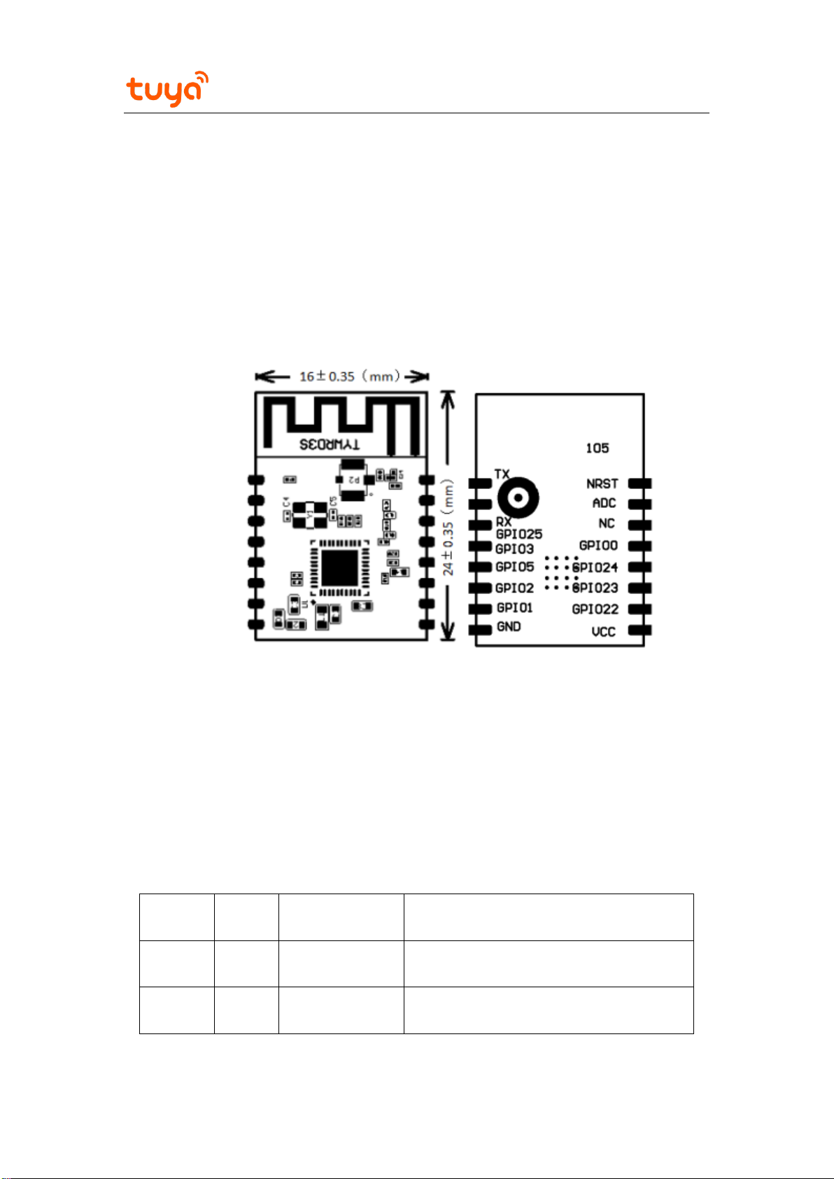
TYWRD3S has two rows of pins with the distance of 2 mm between every two pins.
TYWRD3S dimensions: 16mm±0.35mm(W)×24±0.35mm(L) ×3.5±0.15mm (H)
Figure 1 shows the TYWRD3S dimensions.
Figure 1 TYWRD3S front and back views
2.2 Pin Definition
Table 1 describes the interface pins.
Table 1 TYWRD3S interface pins
No.
Symbol
I/O Type
Function
1
nRST
I/O
Hardware reset pin (active at a low level)
2
ADC
AI
ADC interface
(1)

TYWRD3S Datasheet
Hangzhou Tuya Information Technology Co., Ltd. 6 V2.0.2
3
NC
I
Null pin, no internal connection
4
GPIO0
I/O
GPIO_0,which is connected to GPIO0 on
the IC
5
GPIO23
I/O
GPIO_23, a standard PWM interface,which is
connected to GPIO23 on the IC
6
GPIO24
I/O
GPIO_24, a standard PWM interface,which is
connected to GPIO24 on the IC
7
GPIO25
I/O
GPIO_25, a standard PWM interface,which is
connected to GPIO25 on the IC
8
3.3 V
P
Power supply pin
9
GND
P
Power supply reference ground pin
10
GPIO1
Output
GPIO_1,which is connected to GPIO1 on
the IC
11
GPIO2
Output
UART2_TXD (used to display the module
internal information),which is connected to
GPIO2on the IC
12
GPIO5
I/O
GPIO_5,which is connected to GPIO5 on
the IC
13
GPIO22
I/O
GPIO_22, a standard PWM interface,which is
connected to GPIO22 on the IC
14
GPIO3
I/O
GPIO_3, a standard PWM interface,which is
connected to GPIO3 on the IC
15
RX
I/O
UART_RX
(2),
which is connected to
GPIO27 on the IC
16
TX
Output
UART_TX
(2),
which is connected to
GPIO26 on the IC

TYWRD3S Datasheet
Hangzhou Tuya Information Technology Co., Ltd. 7 V2.0.2
Note: P indicates power-supply pins, I/O indicates input and output pins, and AI indicates
analog input pins.
nRST is only a module hardware reset pin and cannot clear the Wi-Fi network
configuration.
(1) This pin can only be used as an ADC interface and cannot be used as a common
I/O pin. If this pin is not used, it must be disconnected. When this pin is used as the
ADC input interface, the input voltage range is 0 V to 2.0 V.
(2) The UART pins are user-side serial interfaces.
2.3 Test Pin Definition
Table 2 describes the test pins.
Table 2 TYWRD3S test pins
No.
Symbol
I/O Type
Function
1 N/A
Used for the module production test
Note: Test pins cannot be used.
3 Electrical Parameters
3.1 Absolute Electrical Parameters
Table 3 Absolute electrical parameters
Parameter
Description
Minimum
Value
Maximum
Value
Unit
Ts
Storage
temperature
–20
85
°C

TYWRD3S Datasheet
Hangzhou Tuya Information Technology Co., Ltd. 8 V2.0.2
Parameter
Description
Minimum
Value
Maximum
Value
Unit
VBAT
Power supply
voltage
3.0
3.6
V
Static electricity
voltage (human
body model)
Tamb = 25°C
N/A
2
kV
Static electricity
voltage (machine
model)
Tamb = 25°C
N/A
0.5
kV
3.2 Electrical Conditions
Table 4 Normal electrical conditions
Parameter
Description
Minimum
Value
Typical
Value
Maximum
Value
Unit
Ta
Working
temperature
–20
N/A
85
°C
VBAT
Power supply
voltage
3.0
3.3
3.6 V VIL
I/O low-level
input
–0.3
N/A
VCC x 0.3
V
VIH
I/O high-level
input
VCC x 0.75
N/A
VCC
V
VOL
I/O low-level
output
N/A
N/A
VCC x 0.1
V
VOH
I/O high-level
output
VCC x 0.8
N/A
VCC
V
I
max
I/O drive current
N/A
N/A
10
mA

TYWRD3S Datasheet
Hangzhou Tuya Information Technology Co., Ltd. 9 V2.0.2
3.3 Wi-Fi RX Power Consumption
Table 6 RX power consumption during constant receiving
Symbol
Mode
Rate
Typical Value
Unit
I
RF
802.11b
11 Mbit/s
80
mA
I
RF
802.11g
54 Mbit/s
80
mA
I
RF
802.11n
MCS7
80
mA
3.4 Power Consumption in Working Mode
Table 7 TYWRD3S working current
Working Mode
Working Status (Ta = 25°C)
Average
Value
Peak
Value
Unit
EZ mode
The module is in EZ mode.
70
335
mA
AP mode
The module is in AP mode.
80
350
mA
Connected
The module is connected to the network.
70
240
mA
Note: ALL the parameter vary according to the different firmware
4 RF Features
4.1 Basic RF Features
Table 8 Basic RF features

TYWRD3S Datasheet
Hangzhou Tuya Information Technology Co., Ltd. 10 V2.0.2
Parameter
Description
Frequency band
2.4GHz
Wi-Fi standard
IEEE 802.11b/g/n20
Data transmission rate
802.11b: 1, 2, 5.5, or 11 (Mbit/s)
802.11g: 6, 9, 12, 18, 24, 36, 48, or 54 (Mbit/s)
802.11n: HT20 MCS0 to MCS7
Antenna type
Onboard PCB antenna
4.2 Wi-Fi Output Power
Table 9 TX power during constant emission
Parameter
Minimu
m Value
Typical
Value
Maxim
um
Value
Unit
Average RF output power, 802.11b CCK mode
1
Mbit/s
N/A
17
N/A
dBm
Average RF output power, 802.11g OFDM
mode
54
Mbit/s
N/A
14
N/A
dBm
Average RF output power, 802.11n OFDM
mode
MCS7
N/A
12
N/A
dBm
Frequency error
–20
N/A
20
ppm
4.3 Wi-Fi RX Sensitivity
Table 10 RX sensitivity
Parameter
Minimum
Typical
Maximum
Unit

TYWRD3S Datasheet
Hangzhou Tuya Information Technology Co., Ltd. 11 V2.0.2
Value
Value
Value
PER < 8%, 802.11b CCK mode
1 Mbit/s
N/A
–90
N/A
dBm
PER < 10%, 802.11g OFDM mode
54 Mbit/s
N/A
–73
N/A
dBm
PER < 10%, 802.11n OFDM mode
MCS7
N/A
–70
N/A
dBm
5 Antenna Information
5.1 Antenna Type
TYWRD3S uses the onboard PCB antenna.
5.2 Antenna Interference Reduction
To ensure optimal Wi-Fi performance when the Wi-Fi module uses an onboard PCB antenna,
it is recommended that the antenna be at least 15 mm away from other metal parts.
To prevent adverse impact on the antenna performance, do not use copper or route cables
along the antenna area on the PCB.
For details about the onboard PCB antenna area on a module, see Figure 3.
5.3 Antenna Connector Specifications
There is no antenna connector for this module

TYWRD3S Datasheet
Hangzhou Tuya Information Technology Co., Ltd. 12 V2.0.2
6. Packaging Information and Production Instructions
6.1 Mechanical Dimensions
Figure 2 TYWRD3S mechanical dimensions
Figure 3 Side view

TYWRD3S Datasheet
Hangzhou Tuya Information Technology Co., Ltd. 13 V2.0.2
6.2 Recommended PCB Encapsulation
Figure 4 TYWRD3S schematic diagram and pin connection
Figure 5 TYWRD3S encapsulation on the PCB

TYWRD3S Datasheet
Hangzhou Tuya Information Technology Co., Ltd. 14 V2.0.2
6.3 Production Instructions
1. Use an SMT placement machine to mount components to the stamp hole module that
Tuya produces within 24 hours after the module is unpacked and the firmware is
burned. If not, vacuum pack the module again. Bake the module before mounting
components to the module.
(1) SMT placement equipment
i. Reflow soldering machine
ii. Automated optical inspection (AOI) equipment
iii. Nozzle with a 6 mm to 8 mm diameter
(2) Baking equipment
i. Cabinet oven
ii. Anti-static heat-resistant trays
iii. Anti-static heat-resistant gloves
2. Storage conditions for a delivered module are as follows:
(1) The moisture-proof bag is placed in an environment where the temperature is
below 30°C and the relative humidity is lower than 70%.
(2) The shelf life of a dry-packaged product is six months from the date when the
product is packaged and sealed.
(3) The package contains a humidity indicator card (HIC).
Figure 6 HIC for TYWRD3S
3. Bake a module based on HIC status as follows when you unpack the module
package:
(1) If the 30%, 40%, and 50% circles are blue, bake the module for 2 consecutive

TYWRD3S Datasheet
Hangzhou Tuya Information Technology Co., Ltd. 15 V2.0.2
hours.
(2) If the 30% circle is pink, bake the module for 4 consecutive hours.
(3) If the 30% and 40% circles are pink, bake the module for 6 consecutive hours.
(4) If the 30%, 40%, and 50% circles are pink, bake the module for 12 consecutive
hours.
4. Baking settings:
(1) Baking temperature: 125±5°C
(2) Alarm temperature: 130°C
(3) SMT placement ready temperature after natural cooling: < 36°C
(4) Number of drying times: 1
(5) Rebaking condition: The module is not soldered within 12 hours after baking.
5. Do not use SMT to process modules that have unpacked for over three months.
Electroless nickel immersion gold (ENIG) is used for the PCBs. If the solder pads are
exposed to the air for over three months, they will be oxidized severely and dry joints
or solder skips may occur. Tuya is not liable for such problems and consequences.
6. Before SMT placement, take electrostatic discharge (ESD) protective measures.
7. To reduce the reflow defect rate, draw 10% of the products for visual inspection and
AOI before first SMT placement to determine a proper oven temperature and
component placement method. Draw 5 to 10 modules every hour from subsequent
batches for visual inspection and AOI.
6.4 Recommended Oven Temperature Curve
Perform SMT placement based on the following reflow oven temperature curve. The
highest temperature is 245°C.

TYWRD3S Datasheet
Hangzhou Tuya Information Technology Co., Ltd. 16 V2.0.2
Figure 6-6 Oven temperature curve
6.5 Storage Conditions

TYWRD3S Datasheet
Hangzhou Tuya Information Technology Co., Ltd. 17 V2.0.2
7 MDQ and Packing Information
MOQ and packing information
Product
Model
MOQ
Packing
Method
Number of Modules
in Each Reel Pack
Number of Reel
Packs in Each Box
TYWRD3S
3600
Carrier tape
and reel
packing
900
4

TYWRD3S Datasheet
Hangzhou Tuya Information Technology Co., Ltd. 18 V2.0.2
8 Appendix: Statement
Federal Communications Commission (FCC) Declaration ofConformity
FCC Caution: Any changes or modifications not expressly
approved by the party responsible for compliance could void the user's
authority to operate this equipment.
This device complies with Part 15 of the FCC Rules.
Operation is subject to the following two conditions: (1) This device may not
cause harmful interference, and (2) this device must accept any interference
received, including interference that may cause undesired operation.
This device and its antenna(s) must not be co-located or operating in conjunction
with any other antenna or transmitter.
15.105 Information to the user.
(b) For a Class B digital device or peripheral, the instructions furnished the
user shall include the following or similar statement, placed in a prominent
location in the text of the manual:
Note: This equipment has been tested and found to comply
with the limits for a Class B digital device, pursuant to part 15 of the FCC Rules.
These limits are designed to provide reasonable protection against harmful
interference in a residential installation. This equipment generates, uses and
can radiate radio frequency energy and, if not installed and used in
accordance with the instructions, may cause harmful interference to radio
communications. However, there is no guarantee that interference will not
occur in a particular installation. If this equipment does cause harmful
interference to radio or television reception, which can be determined by
turning the equipment off and on, the user is encouraged to try to correct the

TYWRD3S Datasheet
Hangzhou Tuya Information Technology Co., Ltd. 19 V2.0.2
interference by one or more of the following measures:
—Reorient or relocate the receiving antenna.
—Increase the separation between the equipment and receiver.
—Connect the equipment into an outlet on a circuit different from that to which
the receiver is connected.
—Consult the dealer or an experienced radio/TV technician for help.
This equipment complies with FCC radiation exposure limits set forth for an uncont
rolled environment. This equipment should be installed and operated with minimum
distance 20cm between the radiator and your body.
Radiation Exposure Statement:
This equipment complies with FCC radiation exposure limits set forth for an
uncontrolled environment.
This transmitter must not be co-located or operating in conjunction with any other
antenna or transmitter.
The availability of some specific channels and/or operational frequency bands
are country dependent and are firmware programmed at the factory to match
the intended destination.
The firmware setting is not accessible by the end user.
The final end product must be label led in a visible area with the following:
“Contains Transmitter Module 2ANDL-TYWRD3S”
This radio module must not installed to co-locate and operating simultaneously with
other radios in host system, additional testing and equipment authorization may be
required to operating simultaneously with other radio.

TYWRD3S Datasheet
Hangzhou Tuya Information Technology Co., Ltd. 20 V2.0.2
Declaration of Conformity European notice
Hereby, Hangzhou Tuya Information Technology Co., Ltd declares that this WIFI module
product is in compliance with essential requirements and other relevant provisions
of Directive 2014/53/EC. A copy of the Declaration of conformity can be found at
http://www.tuya.com.
EN 300 328 V2.1.1
EN 301 489-1 V2.1.1; EN 301 489-17 V3.1.1
EN 62311:2008
EN 60950-1:2006+A11:2009+A1:2010+A12:2011+A2:2013
 Loading...