


Hangzhou Tuya Inc. NM1 Module Hardware Design Manual
Page1of
29
NM1 Module Hardware Design Manual
NB-IoT Series
Issue: V1.1
Date: 2019-05-06
The Tuya Smart platform is a global intelligent platform, AI and IoT developer platform, and
world-leading voice interaction platform that provides one-stop AI and IoT solutions to meet intelligence
requirements of consumers, manufacturers, OEMs, and retail chain stores. Its solutions cover hardware
access, cloud services, and app software development, forming a closed service loop of AI and
manufacturing. It provides business group technologies and business model upgrade services for
consumer-level smart IoT devices to meet consumers' higher requirements for hardware. Tuya has
always been committed to providing customers with timely and comprehensive services. If you need any
help, contact Tuya headquarters. Tuya's contact information is as follows:
Hangzhou Tuya Inc.
Floor 7, Zheshang Fortune Center, No. 99, Gudun Road, Xihu District, Hangzhou, Zhejiang Province,
China
400-881-8611
https://www.tuya.com

Hangzhou Tuya Inc. NM1 Module Hardware Design Manual
Page2of
29
Date
Version
Change Description
Prepared By
Reviewed By
Approved By
2019-03-01
1.0
This is the first release.
Wang Yanfeng
Wang Yanfeng
Chen Lihuan
Change History
https://www.tuya.com

Hangzhou Tuya Inc. NM1 Module Hardware Design Manual
Page3of
29
Notice
Copyright Statement
Tuya reserves rights for this document and its content, which is protected by Chinese laws and related
copyright laws in applicable international conventions. No part of this document may be reproduced,
transmitted, distributed, or modified in any form or by any means without prior written consent of Tuya.
Those who violate shall be held liable.
Statement of Non-Guarantee
Tuya does not provide guarantees or presentations of any kind, either express or implied for content in
this document and is not reliable for specific merchantability, applicability, and indirect, special, or
associated losses.
Confidentiality Statement
Information, including attachments in this document, is confidential. Those who receive this document
shall know that it is confidential, not use it for other purposes except the specified one, and not disclose
it to any third party.
Disclaimer
Tuya is not reliable for human injuries or property damages caused by misoperations. You shall develop
products based on the technical specifications and reference design provided in this document. The
information in this document is subject to changes without notice.
https://www.tuya.com

Hangzhou Tuya Inc. NM1 Module Hardware Design Manual
Page4of
29
Contents
1 About This Document................................................................................................................................................... 6
1.1 Applicable Scope....................................................................................................................................................6
1.2 Purpose................................................................................................................................................................... 6
1.3 Reference Documents............................................................................................................................................6
1.4 Acronyms and Abbreviations.................................................................................................................................. 6
2 Product Overview..........................................................................................................................................................7
2.1 Package Size...........................................................................................................................................................7
2.2 Technical Parameters...............................................................................................................................................8
2.3 Product Functions................................................................................................................................................. 9
2.3.1 Baseband Functions..................................................................................................................................... 9
2.3.2 RF Functions................................................................................................................................................. 9
3 Interfaces......................................................................................................................................................................11
3.1 Pin Definition....................................................................................................................................................... 11
3.1.1 Pin Symbols..................................................................................................................................................11
3.1.2 Pin Configuration Diagram.......................................................................................................................11
3.1.3 Pins............................................................................................................................................................... 11
3.2 Electrical Conditions............................................................................................................................................. 15
3.3 Power Interface....................................................................................................................................................15
3.3.1 Power Pins and Grounding....................................................................................................................... 15
3.3.2 Power Supply Requirements.....................................................................................................................15
3.4 SIM Card Interface.............................................................................................................................................16
3.4.1 Pins...............................................................................................................................................................16
3.4.2 SIM Card Interface Application...................................................................................................................16
3.5 SPIs........................................................................................................................................................................17
3.5.1 Pins............................................................................................................................................................... 17
3.5.2 SPI Electrical Parameters and Application.................................................................................................. 17
3.6 I2C Interface.........................................................................................................................................................17
3.6.1 Pins...............................................................................................................................................................17
3.6.2 I2C Interface Electrical Parameters and Application.............................................................................18
3.7 UART Interface................................................................................................................................................... 18
3.7.1 Pins............................................................................................................................................................... 18
3.7.2 UART Interface Electrical Parameters and Application.............................................................................. 18
3.8 USB Interface.......................................................................................................................................................19
3.8.1 USB and Downloading Interface Pins (COM Function Not Supported).................................................... 19
3.8.2 USB and Downloading Interface Application............................................................................................. 20
3.9 Power-On/Power-Off and Reset Interface............................................................................................................ 20
3.9.1 PWRKEY Pin...............................................................................................................................................20
3.9.2 Power-On/Power-Off Interface Application................................................................................................ 20
3.9.3 RESET Pin....................................................................................................................................................21
3.9.4 RESET Interface Application.......................................................................................................................21
4 Design Instructions......................................................................................................................................................21
4.1 General Design Rules and Requirements..............................................................................................................21
4.2 Power Supply Circuit Design................................................................................................................................21
4.3 RF Circuit Design................................................................................................................................................ 21
4.3.1 RF Antenna Circuit Design..........................................................................................................................22
4.3.2 Precautions for Initial Antenna Design........................................................................................................ 23
4.4 Suggestions on EMC and ESD Design.................................................................................................................23
4.5 PCB Solder Pad Design.......................................................................................................................................23
4.6 Thermal Design..................................................................................................................................................... 23
5 Production Instructions................................................................................................................................................24
5.1 Stencil Design........................................................................................................................................................24
5.2 Oven Temperature Curve...................................................................................................................................24
6 Mechanical Size...........................................................................................................................................................26
6.1 NM1 Module Mechanical Size............................................................................................................................. 26
6.2 Recommended Package Size.................................................................................................................................28
https://www.tuya.com

Hangzhou Tuya Inc. NM1 Module Hardware Design Manual
Page5of
29
Figures
Figure 2- 1 Product appearance.....................................................................................................................................7
Figure 2- 2 Package size diagram (unit: mm)............................................................................................................... 7
Figure 2- 3 System connection framework................................................................................................................... 9
Figure 3- 1 Pin configuration diagram.........................................................................................................................11
Figure 3- 2 Power supply of the NM1 module............................................................................................................15
Figure 3- 3 SIM card interface application..................................................................................................................16
Figure 3- 4 Reference circuit....................................................................................................................................... 17
Figure 3- 5 Reference circuit....................................................................................................................................... 18
Figure 3- 6 Reference circuit....................................................................................................................................... 18
Figure 3- 7 Reference circuit with a level converter................................................................................................... 19
Figure 3- 8 Reference circuit with a triode for level conversion................................................................................ 19
Figure 3- 9 Downloading interface application circuit............................................................................................... 20
Figure 3- 10 PWRKEY interface application circuit.................................................................................................. 20
Figure 3- 11 RESET interface application circuit....................................................................................................... 21
Figure 4- 1 Antenna impedance calculation model..................................................................................................... 22
Figure 4- 2 Antenna PCB cabling impedance calculation data...................................................................................23
Figure 5- 1 Recommended stencil strips..................................................................................................................... 24
Figure 5- 2 Over temperature curve............................................................................................................................ 25
Figure 6- 1 Top view (unit: mm)................................................................................................................................. 26
Figure 6- 2 Side view (unit: mm)................................................................................................................................ 26
Figure 6- 3 Transparent view (unit: mm).................................................................................................................... 27
Figure 6- 4 Recommended package size (unit: mm)...................................................................................................28
Tables
Table 1- 1 Reference documents....................................................................................................................................6
Table 1- 2 Acronyms and abbreviations........................................................................................................................ 6
Table 2- 1 Technical parameters of the NM1 module................................................................................................... 8
Table 2- 2 Working frequency bands.............................................................................................................................9
Table 2- 3 Line loss requirements................................................................................................................................10
Table 2- 4 Antenna requirements.................................................................................................................................10
Table 2- 5 Conducted RF transmit power....................................................................................................................10
Table 3- 1 Pin symbols.................................................................................................................................................11
Table 3- 2 Interface pin definition............................................................................................................................... 11
Table 3- 3 Electrical conditions...................................................................................................................................15
Table 3- 4 Definition and description of SIM card interface signals..........................................................................16
Table 3- 5 SPI signal definition................................................................................................................................... 17
Table 3- 6 I2C interface signal definition.....................................................................................................................17
Table 3- 7 UART interface signal definition............................................................................................................... 18
Table 3- 8 USB and downloading interface signal definition..................................................................................... 19
Table 3- 9 PWRKEY signal definition........................................................................................................................ 20
Table 3- 10 RESET signal definition...........................................................................................................................21
Table 5- 1 Over temperature curve parameter settings................................................................................................24
https://www.tuya.com

Hangzhou Tuya Inc. NM1 Module Hardware Design Manual
Page6of
29
Document No.
Document Name
NM1 Module Hardware Manual.pdf
NM1 Module Software Manual.pdf
NM1 Module TE-B User Manual.pdf
Acronyms
Full Spelling
ESD
electrostatic discharge
USB
Universal Serial Bus
UART
universal asynchronous receiver/transmitter
SIM
subscriber identity module
SPI
serial peripheral interface
I2C
inter-integrated circuit
I/O
Input/Output
GPIO
General Purpose Input/Output
TDB
To be determined
RTC
real-time clock
ADC
analog to digital converter
1 About This Document
1.1 Applicable Scope
This document describes hardware interface specifications, electrical features, mechanical specifications, and
other related information about the NM1 module to help you design and develop NM1 module hardware.
1.2 Purpose
This document provides NM1 module design and development bases. Through this document, you can know the
NM1 module and its technical parameters and develop related functional product or devices.
In addition to functional features and technical parameters, this document also describes the product reliability
test, related test standards, service function implementation process, RF performance indicators, and circuit
design.
1.3 Reference Documents
Table 1-1 Reference documents
1.4 Acronyms and Abbreviations
Table 1-2 Acronyms and abbreviations
https://www.tuya.com
Hangzhou Tuya Inc. NM1 Module Hardware Design Manual
Page7of
29
2 Product Overview
NM1 is a compact, high-performance, and low-power NB-IoT series module. It has the following features:
Supports the B1, B3,B5,B8, B20 frequency bands.
Provides the SIM card interface (1.8 V), USB 1.1 interface, UART interface, SPI, I2C interface, and GPIO
interface.
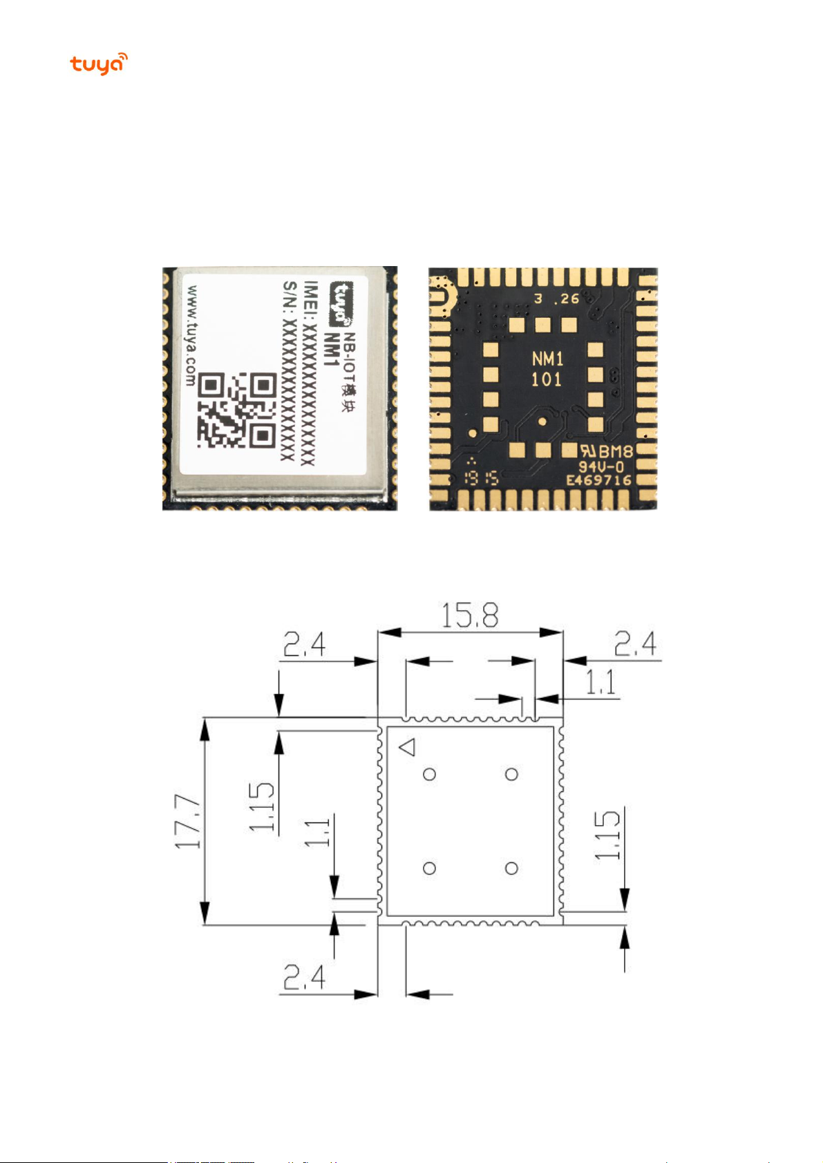
Figure 2- 1 Product appearance
2.1 Package Dimensions
The NM1 module has 66 pins. Its dimensions is 17.7 2.4 mm (H) x 17.7 mm (W) x 15.8 mm (D).
Figure 2- 2 Package dimensions diagram (unit: mm)
https://www.tuya.com
Hangzhou Tuya Inc. NM1 Module Hardware Design Manual
Page8of
29
Item
Parameter
Specifications
Mechanical
features
Package size and type
17.7 mm x 15.8 mm x 2.6 mm
Stamp hole (52 pins) and base pad (14 pins)
Module
Platform
MT2625
Processor architecture
ARM Cortex-M4
SIM card interface
1.8 V
USB interface
USB 1.1
Voltage
2.1 V to 3.63 V
Working mode
Active: The NM1 module is active and can send and receive data. All functions are
available. An active NM1 module can switch to the idle or PSM mode.
Idle: The NM1 module is in idle state, connected to a network, and can receive paging
messages. An idle NM1 module can switch to the active or PSM mode.
PSM: Only RTC of the module works, and the module is disconnected from the network
and cannot receive paging messages.
The NM1 module is woken up from the PSM mode when the timer expires or the
PWRKEY and PSM_EINT* pins are lowered.
Power-saving
In PSM mode, the NM1 module consumes the minimum power of 5 µA. The PSM mode
is provided to reduce power consumption and prolong the power supply duration of the
battery.
Serial port
Primary serial interface: transmits AT commands and data. The default baud rate is 115.2
kbit/s. It can also be used for firmware upgrade and the baud rate is 921.6 kbit/s.
Debugging serial interface: exports log information for software commissioning.
Auxiliary serial interface: transmits AT commands and data.
Working current
TBD
RTC
Supported
ADC*
The NM1 module has a 10-bit analog-digit conversion input interface to measure the
voltage. This interface works in both active and idle modes.
RI signal*
When the NM1 module receives SMS messages or exports URC, it notifies the DTE
over the RI pin.
Network status
indication*
The NETLIGHT signal indicates the module's network connection status.
RF
Frequency band
B1, B3, B5,B8, B20
Maximum TX power
23±2 dBm
Receiving sensitivity
TBD
Main antenna interface
Supported
Antenna interface
Characteristic impedance of 50 ohms. The antenna is provided by a third party, but not
Tuya.
Technical
standard
Data rate
Single-tone: downlink 25.5 kbit/s and uplink 16.7 kbit/s
Multi-tone*: downlink 25.5 kbit/s and uplink 62.5 kbit/s
Network protocol
UDP/TCP/CoAP/LWM2M/PPP*/SSL*/DTLS*/FTP*/HTTP*/MQTT*/HTTPS*
Environment
feature
Temperature
Normal operating temperature: –35°C to +75°C
1
Extended operating temperature: –40°C to +85°C
2
Storage temperature: –40°C to +90°C
Application
SMS*
Text and packet data unit (PDU) modes
Upgrade
Upgrade is performed over the primary serial interface.
2.2 Technical Parameters
Table 2-1 describes mechanical features, baseband features, RF features, technical standards, and environment
features of the NM1 module.
Table 2-1 Technical parameters of the NM1 module
Note:
1. When the NM1 module works at a temperature within the normal operating temperature range1, its performance complies with
https://www.tuya.com
3GPP standards.
2. When the NM1 module works at a temperature within the extended operating temperature range2, it works properly, has the
SMS* and data transmission functions, and will not have unrecoverable faults. The RF spectrum and network are not affected.
Several indicators, for example, the output power, may exceed the 3GPP limits. After the operating temperature is restored to the
normal operating temperature, all NM1 module indicators can meet 3GPP standard requirements.
3. A feature with an asterisk (*) is being developed.
Hangzhou Tuya Inc. NM1 Module Hardware Design Manual
Page9of
29
Working Frequency Band
Uplink (MHz)
Downlink (MHz)
B1
1920–1980
2110–2170
B3
1710–1785
1805–1880
B5
824–849
869-894
B8
880–915
925–960
B20
832–862
791–821
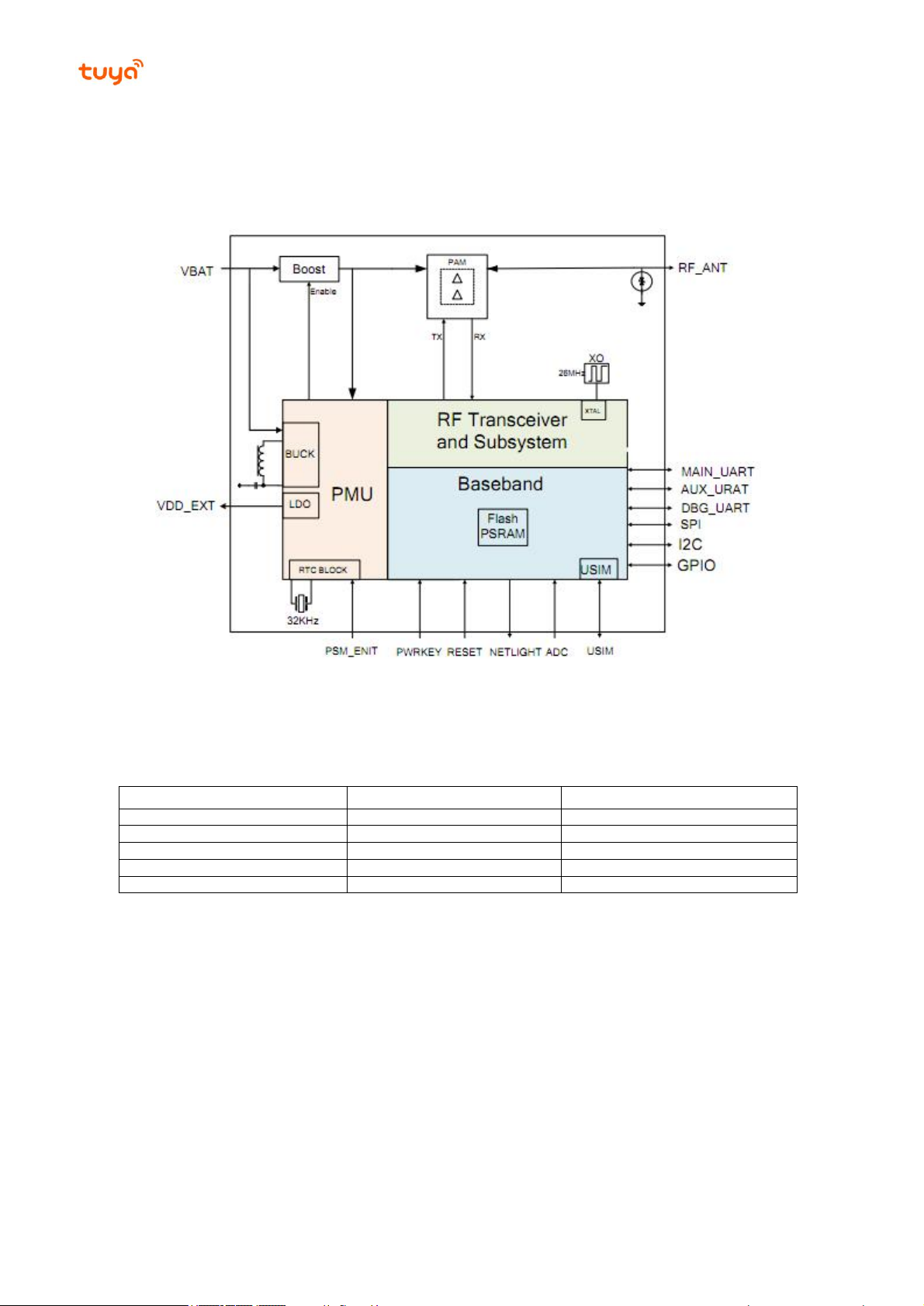
2.3 Product Functions
2.3.1 Baseband Functions
The NM1 module baseband includes the USB interface signal, SIM card interface signal, I2C interface signal,
UART interface signal, working status indicator signal, module startup and reset signals, and multiplexing
control signals, power supply, and grounding of multiple GPIO interfaces.
2.3.2 RF Functions
Note: The NM1 module is being developed to support the frequency bands with an asterisk (*).
Figure 2- 3 System connection framework
Table 2-2 Working frequency bands
https://www.tuya.com
 Loading...