


BT3L-G Datasheet
Tuya BT3L-G BLE Module
Date: 2019-10-24
No.: 0000000001
Product
Manual
Global Intelligent Platform
Version: 1.0.0
1 Product Overview
BT3L-G is an embedded Bluetooth Low Energy (BLE) module that Tuya has developed. It
consists of a highly integrated Bluetooth chip (TLSR8250F512GT32) and several
peripheral circuits, with an embedded Bluetooth network protocol stack and robust library
functions. BT3L-G also contains a low-power 32-bit multipoint control unit (MCU), BLE 5.0
or 2.4 GHz radio, 4 MB flash memory, 48 KB static random-access memory (SRAM), and
nine multiplexing I/O pins.
1.1 Features
Embedded low-power 32-bit MCU, which can also function as an application
processor
Clock rate: 48 MHz
Working voltage: 1.8 V to 3.6 V (Under 1.8 V to 2.7 V, the module can start but the RF
performance is not guaranteed. Under 2.8 V to 3.6 V, the module performance is
normal.)
Peripherals: nine pulse width modulation (PWM) pins
BLE RF features
Compatible with BLE 5.0
Up to 2 Mbit/s RF data rate
TX power: +10 dBm
RX sensitivity: –94.5 dBm at BLE 1 Mbit/s
Embedded Advanced Encryption Standard (AES) hardware encryption
Onboard PCB antenna
Working temperature: –20°C to +105°C
1

1.2 Applications
Smart LED lights
Smart households
Smart low-power sensors
BT3L-G Datasheet
2

Change History
No.
Date
Change Description
Version After Change
1
2019-10-24
This is the first release.
1.0.0
BT3L-G Datasheet
3

BT3L-G Datasheet
Contents
1 Product Overview.....................................................................................................................1
1.1 Features.........................................................................................................................1
1.2 Applications...................................................................................................................2
2 Module Interfaces.....................................................................................................................6
2.1 Dimensions and Footprint...........................................................................................6
2.2 Interface Pin Definition................................................................................................ 6
3 Electrical Parameters.............................................................................................................. 9
3.1 Absolute Electrical Parameters................................................................................. 9
3.2 Electrical Conditions....................................................................................................9
3.3 Power Consumption..................................................................................................10
4 RF Features............................................................................................................................ 11
4.1 Basic RF Features..................................................................................................... 11
4.2 RF TX Power...............................................................................................................11
4.3 RF RX Sensitivity.......................................................................................................12
5 Antenna Information..............................................................................................................12
5.1 Antenna Type..............................................................................................................12
5.2 Antenna Interference Reduction............................................................................. 12
6 Packaging Information and Production Instructions........................................................ 13
6.1 Mechanical Dimensions and Rear Solder Pad Dimensions...............................13
6.2 Production Instructions............................................................................................. 13
6.3 Recommended Oven Temperature Curve.............................................................15
6.4 Storage Conditions....................................................................................................17
7 MOQ and Packing Information............................................................................................ 18
8 Appendix: Statement.............................................................................................................18
4

BT3L-G Datasheet
Figures
Figure 2-1 BT3L-G front and rear views.............................................................................. 6
Figure 6-1 BT3L-G mechanical dimensions and rear solder pad dimensions............ 13
Figure 6-2 HIC for BT3L-G...................................................................................................14
Figure 6-3 Oven temperature curve................................................................................... 16
Tables
Table 2-1 BT3L-G interface pins............................................................................................6
Table 3-1 Absolute electrical parameters.............................................................................9
Table 3-2 Normal electrical conditions..................................................................................9
Table 3-3 Power consumption in different working modes............................................. 10
Table 4-1 Basic RF features.................................................................................................11
Table 4-2 Power during constant transmission................................................................. 11
Table 4-3 RX sensitivity.........................................................................................................12
5
BT3L-G Datasheet
Pin
No.
Symbol
I/O
Type
Function
1
RST
I/O
Hardware reset pin, which is active at a low level and
is connected to the RESETB pin on the internal IC
2
ADC
AI
12-bit ADC pin, which is connected to the TL_C4 pin
on the internal IC
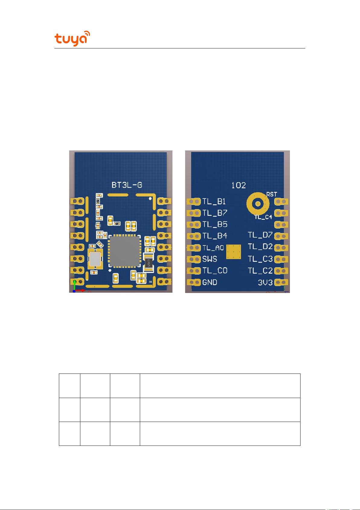
2 Module Interfaces
2.1 Dimensions and Footprint
BT3L-G has two rows of pins with a 2 mm pin spacing.
The BT3L-G dimensions (H x W x D) are 3.3±0.15 mm x 16±0.35 mm x 24±0.35 mm. The
PCB thickness is 0.8±0.1 mm. Figure 2-1 shows the BT3L-G front and rear views.
Figure 2-1 BT3L-G front and rear views
2.2 Interface Pin Definition
Table 2-1 BT3L-G interface pins
6

BT3L-G Datasheet
Pin
No.
Symbol
I/O
Type
Function
3NCI/O
NC
4
TL_D7
I/O
GPIO, which is connected to the TL_D7 pin on the
internal IC
5
TL_D2
I/O
Common I/O pin, which can be used as a PWM
output of the LED drive and is connected to the
TL_D2 pin on the internal IC
6
TL_C3
I/O
Common I/O pin, which can be used as a PWM
output of the LED drive and is connected to the
TL_C3 pin on the internal IC
7
TL_C2
I/O
Common I/O pin, which can be used as a PWM
output of the LED drive and is connected to the
TL_C2 pin on the internal IC
8
VDD_
BAT
P
Power supply pin (3.3 V)
9
GND
P
Power supply reference ground pin
10
TL_C0
I/O
GPIO, which is connected to the TL_C0 pin on the
internal IC
11
SWS
Input
Programming pin, which is connected to the TL_D4
pin on the internal IC
12
TL_A0
I/O
GPIO, which is connected to the TL_A0 pin on the
internal IC
13
TL_B4
I/O
Common I/O pin, which can be used as a PWM
output of the LED drive and is connected to the
TL_B4 pin on the internal IC
14
TL_B5
I/O
Common I/O pin, which can be used as a PWM
output of the LED drive and is connected to the
TL_B5 pin on the internal IC
15
TL_B7
I/O
Serial interface receiving pin (UART RX), which is
connected to the TL_B7 pin on the internal IC
16
TL_B1
I/O
Serial interface transmission pin (UART TX), which is
connected to the TL_B1 pin on the internal IC
7

BT3L-G Datasheet
Note:
1. P indicates power supply pins, I/O indicates input/output pins, and AI indicates analog
input pins.
2. If you have special requirements for light colors controlled by PWM outputs, contact
Tuya business personnel.
8

3 Electrical Parameters
Parameter
Description
Minimum
Value
Maximum
Value
Unit
Ts
Storage
temperature
–65
150
°C
VCC
Power supply
voltage
–0.3
3.9
V
Static electricity voltage
(human body model)
Tamb = 25°C
N/A2kV
Static electricity voltage
(machine model)
Tamb = 25°C
N/A
0.5
kV
Parameter
Description
Minimum
Value
Typical
Value
Maximum
Value
Unit
Ta
Working
temperature
–40
N/A
105
°C
VCC
Working voltage
2.8
3.3
3.6
V
VILI/O low-level input
VSS
N/A
VCC x 0.3
V
VIHI/O high-level input
VCC x 0.7
N/A
VCC
V
VOLI/O low-level output
VSS
N/A
VCC x 0.1
V
VOHI/O high-level
output
VCC x 0.9
N/A
VCC
V
3.1 Absolute Electrical Parameters
Table 3-1 Absolute electrical parameters
BT3L-G Datasheet
3.2 Electrical Conditions
Table 3-2 Normal electrical conditions
9

3.3 Power Consumption
Symbol
Description
Typical Value
Unit
I
tx
Constant transmission,
0 dBm output power
6.6
mA
IrxConstant receiving
6.3
mA
IDCConnected to a mesh network
7.3
mA
I
deepsleep1
Deep sleep mode 1
(16 KB RAM is reserved.)
1.2
μA
I
deepsleep2
Deep sleep mode 2
(No RAM is reserved.)
0.4
μA
Table 3-3 Power consumption in different working modes
BT3L-G Datasheet
10

4 RF Features
Parameter
Description
Frequency band
2.4 GHz ISM band
Wireless standard
BLE 4.2 or 5.0
Data transmission rate
1 Mbit/s or 2 Mbit/s
Antenna type
Onboard PCB antenna
Parameter
Minimum
Value
Typical
Value
Maximum
Value
Unit
Average RF output power
–221010.5
dBm
20 dB modulation signal
bandwidth (1 Mbit/s)
N/A
2500
N/A
kHz
20 dB modulation signal
bandwidth (2 Mbit/s)
N/A
1400
N/A
kHz
4.1 Basic RF Features
BT3L-G Datasheet
Table 4-1 Basic RF features
4.2 RF TX Power
Table 4-2 Power during constant transmission
11

4.3 RF RX Sensitivity
Parameter
Minimum
Value
Typical
Value
Maximum
Value
Unit
RX sensitivity
1 Mbit/s
N/A
–94.5
N/A
dBm
2 Mbit/s
N/A
–91
N/A
Frequency offset error
1 Mbit/s
–250
N/A
+300
kHz
2 Mbit/s
–300
N/A
+200
Co-channel interference
suppression
N/A
N/A
–10
N/A
dB
BT3L-G Datasheet
Table 4-3 RX sensitivity
5 Antenna Information
5.1 Antenna Type
BT3L-G uses an onboard PCB antenna.
5.2 Antenna Interference Reduction
To ensure optimal RF performance, it is recommended that the antenna be at least 15 mm
away from other metal parts. If metal materials are wrapped around the antenna, the
wireless signals will be reduced greatly, deteriorating the RF performance. As a dual
in-line package (DIP), BT3L-G is through-hole mounted onto the PCB. Sufficient space
needs to be reserved for the antenna.
12

BT3L-G Datasheet
6 Packaging Information and Production Instructions
6.1 Mechanical Dimensions and Rear Solder Pad Dimensions
Figure 6-1 BT3L-G mechanical dimensions and rear solder pad dimensions
Note: The default dimensional tolerance is ±0.35 mm, and the tolerance for some
measurements is ±0.1 mm. If a customer has other requirements, clearly specify them in
the datasheet after communication.
6.2 Production Instructions
1. Use an SMT placement machine to mount the stamp hole module that Tuya produces
onto the PCB within 24 hours after the module is unpacked and the firmware is
burned. If not, vacuum pack the module again. Bake the module before mounting it
onto the PCB.
13
BT3L-G Datasheet
(1) SMT placement equipment
i. Reflow soldering machine
ii. Automated optical inspection (AOI) equipment
iii. Nozzle with a 6 mm to 8 mm diameter
(2) Baking equipment
i. Cabinet oven
ii. Anti-static heat-resistant trays
iii. Anti-static heat-resistant gloves
2. Storage conditions for a delivered module are as follows:
(1) The moisture-proof bag is placed in an environment where the temperature is
below 30°C and the relative humidity is lower than 70%.
(2) The shelf life of a dry-packaged product is six months from the date when the
product is packaged and sealed.
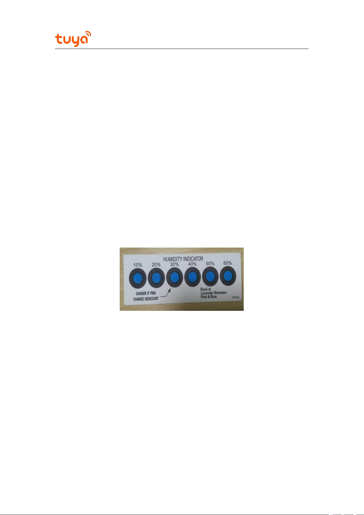
(3) The package contains a humidity indicator card (HIC).
Figure 6-2 HIC for BT3L-G
3. Bake a module based on HIC status as follows when you unpack the module
package:
(1) If the 30%, 40%, and 50% circles are blue, bake the module for 2 consecutive
hours.
(2) If the 30% circle is pink, bake the module for 4 consecutive hours.
(3) If the 30% and 40% circles are pink, bake the module for 6 consecutive hours.
(4) If the 30%, 40%, and 50% circles are pink, bake the module for 12 consecutive
hours.
14

BT3L-G Datasheet
4. Baking settings:
(1) Baking temperature: 125±5°C
(2) Alarm temperature: 130°C
(3) SMT placement ready temperature after natural cooling: < 36°C
(4) Number of drying times: 1
(5) Rebaking condition: The module is not soldered within 12 hours after baking.
5. Do not use SMT to process modules that have been unpacked for over three months.
Electroless nickel immersion gold (ENIG) is used for the PCBs. If the solder pads are
exposed to the air for over three months, they will be oxidized severely and dry joints
or solder skips may occur. Tuya is not liable for such problems and consequences.
6. Before SMT placement, take electrostatic discharge (ESD) protective measures.
7. To reduce the reflow defect rate, draw 10% of the products for visual inspection and
AOI before first SMT placement to determine a proper oven temperature and
component placement method. Draw 5 to 10 modules every hour from subsequent
batches for visual inspection and AOI.
6.3 Recommended Oven Temperature Curve
Perform SMT placement based on the following reflow oven temperature curve. The
highest temperature is 245°C.
Based on the IPC/JEDEC standard, perform reflow soldering on a module at most twice.
15

BT3L-G Datasheet
Figure 6-3 Oven temperature curve
16

6.4 Storage Conditions
BT3L-G Datasheet
17

BT3L-G Datasheet
MOQ and packing information
Product
Model
MOQ
Packing
Method
Number of
Modules in Each
Reel Pack
Number of Reel
Packs in Each Box
BT3L-G
3600
Carrier tape
and reel
packing
900
4
7 MOQ and Packing Information
8 Appendix: Statement
Federal Communications Commission (FCC) Declaration of Conformity
FCC Caution: Any changes or modifications not expressly approved by the party
responsible for compliance could void the user's authority to operate this equipment.
This device complies with Part 15 of the FCC Rules.
Operation is subject to the following two conditions: (1) This device may not cause harmful
interference, and (2) this device must accept any interference received, including
interference that may cause undesired operation.
This device and its antenna(s) must not be co-located or operating in conjunction with any
other antenna or transmitter.
15.105 Information to the user.
(b) For a Class B digital device or peripheral, the instructions furnished the user shall
include the following or similar statement, placed in a prominent location in the text of the
manual:
Note: This equipment has been tested and found to comply with the limits for a Class B
digital device, pursuant to part 15 of the FCC Rules.
These limits are designed to provide reasonable protection against harmful interference in
a residential installation. This equipment generates, uses and can radiate radio frequency
energy and, if not installed and used in accordance with the instructions, may cause
harmful interference to radio communications. However, there is no guarantee that
interference will not occur in a particular installation. If this equipment does cause harmful
18

BT3L-G Datasheet
interference to radio or television reception, which can be determined by turning the
equipment off and on, the user is encouraged to try to correct the interference by one or
more of the following measures:
—Reorient or relocate the receiving antenna.
—Increase the separation between the equipment and receiver.
—Connect the equipment into an outlet on a circuit different from that to which the
receiver is connected.
—Consult the dealer or an experienced radio/TV technician for help.
This equipment complies with FCC radiation exposure limits set forth for an uncontrolled
environment. This equipment should be installed and operated with minimum distance 20
cm between the radiator and your body.
Radiation Exposure Statement:
This equipment complies with FCC radiation exposure limits set forth for an uncontrolled
environment.
This transmitter must not be co-located or operating in conjunction with any other antenna
or transmitter.
The availability of some specific channels and/or operational frequency bands are country
dependent and are firmware programmed at the factory to match the intended destination.
The firmware setting is not accessible by the end user.
The final en
"Contains T
This r
radios
opera
ransmitter Mo
ad
io mo
in host s
tin
g simu
d
product mu
dule m
yste
m, ad
ltane
st be label
dule FCC ID:2A
ust no
t installed
dition
ously
with
al test
other
led in a visi
NDL
to c
o-loca
ing a
nd eq
radio
.
ble area w
-BT3L-G"
te and ope
uipment au
ith the follo
rating
simult
thori
zation
wing:
aneously
may be req
with o
uire
ther
d to
19

Declaration of Conformity European notice
BT3L-G Datasheet
Hereby, Hangzhou Tuya
module product is in com
of Directive 2014/53/EU.
https://www.tuya.com.
Information Technology Co., Ltd declares th
pliance with essential requirements and oth
A copy of the Declaration of conformity can
at this Bluetooth
er relevant provisions
be found at
20
 Loading...