

Model
Antenna type
Note
BL3358-P
PCB antenna
Default
Embedded
Version:1.1 Release date: May 24, 2019
BL3358-P
WiFi Module
Features
192MHz ARM Cortex M4 MCU
384KB SRAM/1MB FLASH
Support AES,MD5,SHA1
Support XIP
Working voltage: DC 3.3V
Wi-Fi related features
Support 802.11 b/g/n with 20M
and 40M bandwidth
Support station and soft AP
Support SmartConfig and AP
configuration
Support WEP/WPA2
Working temperature: -10℃ to +80℃
Stamp style SMD for surface mounting
production
Applications
Smart transportation
Smart home / appliances
Instruments
Health care
Industrial automation
Intelligent security
Smart energy
Support multiple cloud services
Integrated balun/PA/LNA
TCP/IP stack optimized for IoT
application
PCB antenna
Peripheral
3x UART
1x I2C
1x SPI
5x PWM
Up to 10x GPIOs
Model

- 1 -
Content
1. Overview ............................................................................................................................ - 2 -
2. Basic Specifications ............................................................................................................ - 2 -
2.1. Power Consumption ................................................................................................... - 2 -
2.2. Working Environment ................................................................................................ - 3 -
3. Radio Specifications ........................................................................................................... - 3 -
3.1. Basic Radio Specification ............................................................................................ - 3 -
3.2. Radio Performance ..................................................................................................... - 4 -
3.2.1. IEEE 802.11b ........................................................................................................ - 4 -
3.2.2. IEEE 802.11g ........................................................................................................ - 5 -
3.2.3. IEEE802.11n ......................................................................................................... - 6 -
3.2.4. Testing Data for OTA ........................................................................................... - 7 -
Refer to Table 1 for testing data. ...................................................................................... - 7 -
4. BL3358-P Hardware Information ....................................................................................... - 9 -
4.1. PIN Sequence .............................................................................................................. - 9 -
4.2. PIN Definitions ............................................................................................................ - 9 -
4.3. PCB Antenna ............................................................................................................. - 12 -
4.4. Mechanical Dimensions ............................................................................................ - 13 -
4.5. Recommended Pad Size ........................................................................................... - 14 -
4.6. Certifications ............................................................................................................ - 14 -
4.7. Label ......................................................................................................................... - 15 -
4.8. Shielding Case Dimensions ....................................................................................... - 16 -
4.9. Packaging .................................................................................................................. - 16 -
5. Reference Design ............................................................................................................. - 17 -
5.1. UART Interface Design .............................................................................................. - 17 -
5.2. Power Supply Requirement ...................................................................................... - 17 -
Revision History ................................................................................................................... - 21 -
Copyrights ............................................................................................................................ - 22 -
Contact Us ........................................................................................................................... - 22 -
- 2 -
Specifications
Min.
Typ.
Max.
Units
VDD
3
3.3
3.6 V VCC_RTC
1.7
3.3
3.6
V
VIL(input low voltage)
0 0.8 V VIH(input high voltage)
2 3.6 V VOL(output low voltage)
0 0.4 V VOH(output high voltage)
2.4 3.6 V RPU
40 190
KΩ
RPD
40 190
KΩ
Io 8
24
mA
Standby (SP mini)
50 mA
pulse current @TX
11b @18dBm 11Mbps
280
mA
1. Overview
BL3358-P is a cost-effective embedded Wi-Fi module designed by BroadLink, which
integrates an ARM Cortex-M4F processor speed up to 125MHz, 256KB SRAM and 2MB flash with
3.3V single power supply.
The module integrates radio transceiver, MAC, baseband, all Wi-Fi protocols, configurations
and network stack. It can be widely used in applications like smart home devices, remote
monitoring devices and medical care instruments.
2. Basic Specifications
2.1. Power Consumption
Please refer to Table 1 for power consumption data.
Table 1 BL3358-P Power Consumption Data
- 3 -
pulse current @TX
11g @16dBm 54Mbps
280
mA
pulse current @TX
11n @15dBm 65Mbps
230
mA
Symbol
Description
Min.
Max.
Units
Ts
Storage temperature
-40
125 ℃ TA
Ambient operating temperature
-10
80 ℃ Vdd
Supply voltage
3.0
3.6
V
Vio
Voltage on IO pin
0
3.3
V
Radio range
2.412 GHz - 2.472 GHz
Wireless standards
IEEE 802.11 b/g/n
Radio output (conductive)
802.11b:17±1.5dBm@11Mbps
802.11b: 17±1.5dBm@1Mbps
802.11g: 15±1.5dBm@54Mbps
802.11g: 15±1.5dBm@6Mbps
802.11n: 14±1.5dBm@MCS7/HT20
802.11n: 14±1.5dBm@MCS0/HT20
2.2. Working Environment
Please refer to Table 2 for working environment data.
Table 2 BL3358-P Working Environment Data
3. Radio Specifications
3.1. Basic Radio Specification
Please refer to Table 3 for radio specification.
Table 3 BL3358-P Radio Specification
- 4 -
Antenna type
Internal: PCB antenna
External: Not supported
Receiving sensitivity
802.11b<-83dBm@11Mbps
802.11g<-73dBm@54Mbps
802.11n/HT20<-71dBm@MCS7
802.11n/HT40<-69dBm@MCS7
Stack
IPv4, TCP/UDP/FTP/HTTP/HTTPS/TLS/mDNS
Data rate (max)
11M@802.11b, 54M@802.11g, MCS7@802.11n
Security
Encryption standard: Open/WEP-Open/WPA/WPA2
Encryption algorithm: WEP64/WEP128/TKIP/AES
Network types
STA/AP/STA+AP/WIFI Direct
ITEM
Specification
Modulation Type
DSSS / CCK
Frequency range
2412MHz~2462MHz
Channel
CH1 to CH13
Data rate
1, 2, 5.5, 11Mbps
TX Characteristics
Min.
Typical
Max.
Unit
Power@11Mbps
17 dBm
Frequency Error
-10 +10
ppm
EVM@11Mbps
-21
dB
Transmit spectrum mask
Pass
3.2. Radio Performance
3.2.1. IEEE 802.11b
Table 4 Basic specifications under IEEE802.11b
Table 5 Transmitting performance under IEEE802.11b
- 5 -
RX Characteristics
Min
.
Typical
Max.
Unit
11Mbps Input Level Sensitivity
Minimum Input Level (FER≦8%)
-83
dBm
Maximum Input Level (FER≦8%)
-10
dBm
ITEM
Specification
Modulation Type
OFDM
Frequency range
2412MHz~2462MHz
Channel
CH1 to CH13
Data rate
6, 9, 12, 18, 24, 36, 48, 54Mbps
TX Characteristics
Min.
Typical
Max.
Unit
Power@54Mbps
15 dBm
Frequency Error
-10 +10
ppm
EVM@54Mbps
-32
dB
Transmit spectrum mask
Pass
RX Characteristics
Min
.
Typical
Max.
Unit
54Mbps Input Level Sensitivity
Table 6 Receiving performance under IEEE802.11b
3.2.2. IEEE 802.11g
Table 7 Basic specifications under IEEE802.11g
Table 8 Transmitting performance under IEEE802.11g
Table 9 Receiving performance under IEEE802.11g
- 6 -
Minimum Input Level (FER≦10%)
-71.5
dBm
Maximum Input Level (FER≦10%)
-10
dBm
ITEM
Specification
Modulation Type
OFDM
Frequency range
2412MHz~2462MHz
Channel
CH1 to CH13
Data rate
MCS0/1/2/3/4/5/6/7
TX Characteristics
Min.
Typical
Max.
Unit
Power@HT20, MCS7
14 dBm
Frequency Error
-10 +10
ppm
EVM@HT20, MCS7
-32
dB
Transmit spectrum mask
Pass
RX Characteristics
Min
.
Typical
Ma
x.
Unit
MCS7 Input Level Sensitivity
Minimum Input Level (FER≦10%)
-71
dBm
Maximum Input Level (FER≦10%)
-20
dBm
3.2.3 IEEE802.11n
IEEE802.11n 20MHz bandwidth mode
Table 10Basic specifications under IEEE802.11n with 20MHz
Table 11 Transmitting performance under IEEE802.11n with 20MHz
Table 12 Receiving performance under IEEE802.11n with 20MHz

- 7 -
ITEM
Specification
Modulation Type
OFDM
Frequency range
2422MHz~2452MHz
Channel
CH1 to CH13
Data rate
MCS0/1/2/3/4/5/6/7
TX Characteristics
Min.
Typical
Max.
Unit
Power@HT40, MCS7
14 dBm
Frequency Error
-10 +10
ppm
EVM@HT40, MCS7
-33
dB
Transmit spectrum mask
Pass
RX Characteristics
Min
.
Typical
Max.
Unit
MCS7 Input Level Sensitivity
Minimum Input Level (FER≦10%)
-69
dBm
Maximum Input Level (FER≦10%)
-20
dBm
IEEE802.11n 40MHz bandwidth mode
Table 13Basic specifications under IEEE802.11n with 40MHz
Table 14 Transmitting performance under IEEE802.11n with 40MHz
Table 15 Receiving performance under IEEE802.11n with 40MHz
3.2.4 Testing Data for OTA
Refer to Table 1 for testing data.

- 8 -
Testing
equipment
Testing item
Mode
Speed
Chann
el
Power/dB
m
CMW500
EIRP
11b
11M
1
<20 6 <20
13
<20
11g
6M
1
<20 6 <20
13
<20
TRP
11g
6M
1
≥12 6 ≥12
13
≥12
TIS
11g
54M
1
≤-72
6
≤-72
13
≤-72
Table 16 Actual power for EIRP, TRP and TIS

- 9 -
PIN
Function1
2 3 4
Descript
1
GPIO12
TX2
2 GPIO11
RX2
3 GPIO14
PWM4
4. BL3358-P Hardware Information
4.1. PIN Sequence
Please refer to Fig 1 for the pin sequence.
Fig 1 BL3358-P pin sequence
4.2. PIN Definitions
Please refer to Table17 for the pin definitions.
Table17 BL3358-P pin definitions
- 10 -
4
GPIO13
5 GPIO15
PWM3
6 GPIO17
PWM5
7 GPIO2
RX1
PWM0
8 VDD
3.3V
9
GND
10
CHIP_EN
11
GPIO4
12
GPIO3
TX1
13
GPIO1
PWM1
I2C_SDA
14
GPIO0
I2C_SCL
15
GPIO16
16
GPIO21
RX0
17
GPIO22
TX0
18
GND
19
RTC_3V3
RTC_3V3
20
RTC_EINT
RTC_EINT
21
EXT_POW_EN
EXT_POW_EN
Note:
1. In default, UART0 is used for bypass communication and UART2 is used for output of
debugging information. Please refer to the description in DC Characteristics for UART output

- 11 -
PIN
Description
GPIO17
0:XO input is 26M (default)
1: XO input is 40M
GPIO14
0: 32k source is from external
1: 32k source is from internal (default)
GPIO16
0: boot up bypass boot ROM
1: boot up with boot ROM (default)
GPIO15
0: JTAG pin fixed for JTAG
1: JTAG pin as GPIO (default)
GPIO4
0: Boot with host interface disabled (default)
1: Boot with host interface enabled
Active if GPIO4=1
GPIO13
0: Host interface via SPI slave
1: Host interface via SDIO slave (default)
GPIO12
0: enter UART download mode
1: skip UART download (default)
current level.
2. NRST is hardware reset for the module and will be effective with VIL. Configuration
information will be remained after module reset. The module is already designed with RC reset
upon power-on.
3. The pins for reset button and LED indication should be defined according to actual
firmware and circuit design.
4. In default, PIN11 (GPIO2) is the module software reset PIN and will be effective with
VIH. The previous configuration information will be cleared after the module is reset (reset to
factory settings).
5. TX and RX in UART0 are used for communication with external MCU powered by 3V.
Please refer to the description in 3.3. DC Characteristics for UART output current level.
6. It is recommended to ground unused GPIOs with 10pF capacitor.
7. GPIOA0 and GPIOA19 are Power on Trap Pin with functions described below:
The module will detect GPIO0 and GPIO19 when powered on and enter specific mode
according to the IO state.

- 12 -
4.3. PCB Antenna
Please refer to Fig 2 for PCB antenna.
Fig 2 BL3358-P Antenna layout
The module support PCB antenna in 2.4G~2.5G frequency with S11 port less than -10dB and
max gain of 1.5dBi at 2.45GHz, as shown in Fig 3.
Fig 3 Simulated radiation pattern of antenna gain
Please refer to Fig 4 for real testing environment for module antenna.
Fig 4 Antenna testing environment

- 13 -
The following precautions should be considered during designing with PCB antenna:
Do not place any electrical components or grounding in antenna area on main board and it’s
better to leave this area blank on PCB.
It is recommended to not place any electrical components within 10mm range of module
antenna and not design any circuit or bond copper on main board under this area.
Do not use the module inside any metal case or containers with metal painting.
Keep the antenna of wifi module next to the edge of main board (as shown in Fig 5) during
design of PCB to ensure better performance of antenna.
Fig 5 BL3358-P Recommended PCB layout
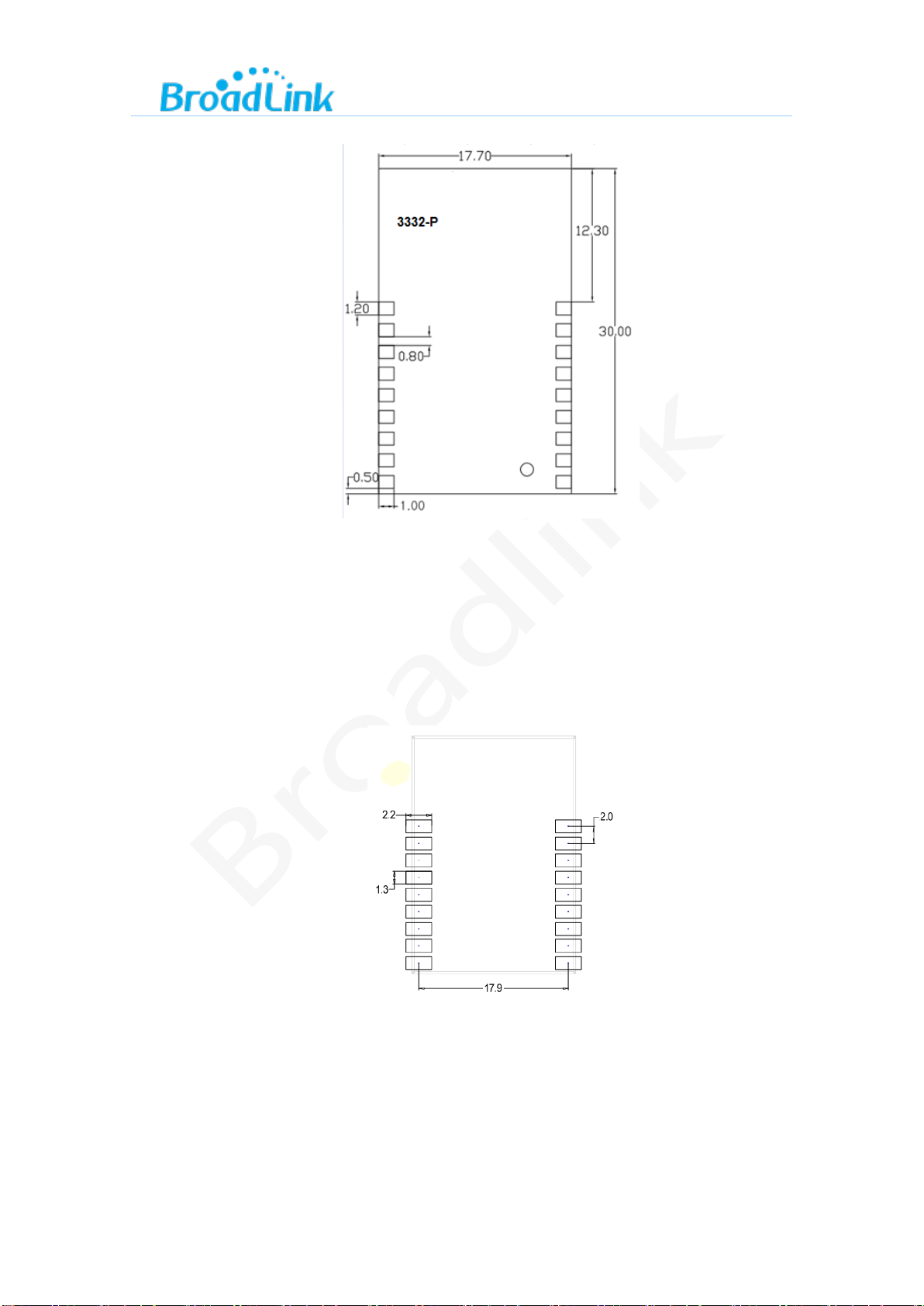
4.4. Mechanical Dimensions
Please refer to Fig 6 for the dimensions of module.
- 14 -
Fig 6 BL3358-P Dimensions
Note: Dimensions (17.7±0.2) mm * (30±0.2) mm * (3.8)mm (with shielding case)
4.5. Recommended Pad Size
Please refer to Fig 7 for the recommended pad size
Fig 7 BL3358-P Recommended pad size
4.6. Certifications
1. Compliant and certified with SRRC standard (CMIIT ID: 2017DP6839).

- 15 -
2. Compliant with requirement of RoHS 2.0.
3. Compliant with requirement of REACH.
4.7. Label
Fig 8 BL3358-P label content
Please refer to Fig 8 for the content description on label.
Model: ******* : Module model
SN: 00ACA3FE75D7 : Module unique MAC address
The QR code contains information including but not limited to:
CMIIT ID:xxxxxxxxxxxxx
FCC ID: 2ATEV-BL3358-P
IC: 25062-BL3358P
Manufacturer:
Hangzhou BroadLink Technology Co., Ltd.
Building C, 57 Jiang’er Road, Binjiang District, Hangzhou, Zhejiang, P.R.China

- 16 -
4.8. Shielding Case Dimensions
Please refer to Fig 9 for the dimensions of shielding case.
Fig 9 BL3358-P Dimensions of shielding case
4.9. Packaging
Please refer to Fig 10 and Fig 11 for the details of packaging.
BL3358-P is packed in reel with 850 pcs/reel
(Unit: mm)
- 17 -
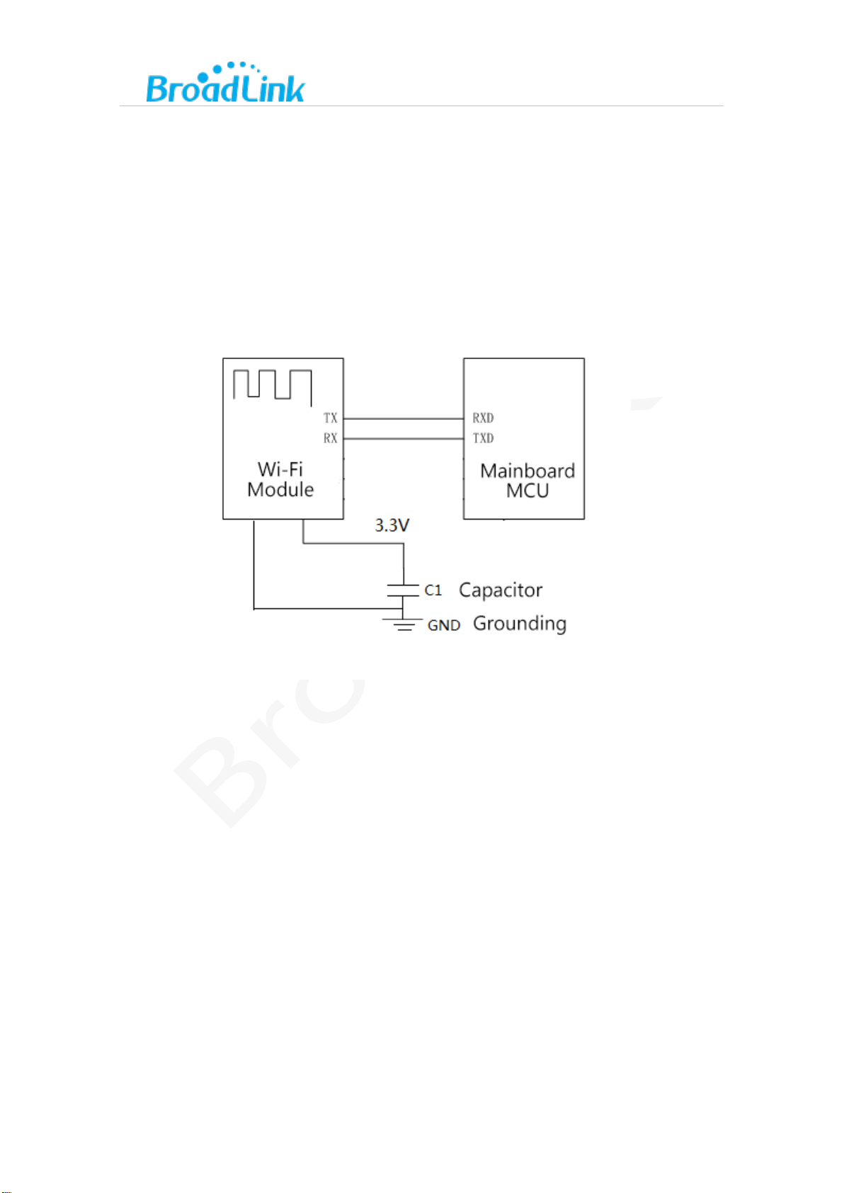
5. Reference Design
5.1. UART Interface Design
For devices with 3.3V power supply, you can directly connect the device UART port with
module UART port according to the illustration in Fig 12.
Fig 12 Circuit diagram (3.3V)
If your device is powered by 5V, you can refer to the circuit shown in Fig 13 or design your
own circuit for power conversion. The value of resistor can be adjusted according to actual circuit
design.
5.2. Power Supply Requirement
If an LDO is used to supply the module with 3.3V power, C1 capacitor can be considered to
be used with 10u-22u; If a DCDC is used to supply 3.3V power, C1 capacitor can be considered to
be used with 22uF.
It is recommended to supply the module with power higher than 400mA to ensure enough
power supply to the module and avoid power down during data transmission.

- 18 -
The module is designed with 2x 3.3V pins. You can power the module with either pin or both
pins.
This device complies with Part 15 of the FCC Rules. Operation is subject to the following two
conditions:
(1) This device may not cause harmful interference, and
(2) This device must accept any interference received, including interference that may cause
undesired operation.
Note: This product has been tested and found to comply with the limits for a Class B digital
device, pursuant to Part 15 of the FCC Rules. These limits are designed to provide reasonable
protection against harmful interference in a residential installation. This product generates, uses,
and can radiate radio frequency energy and, if not installed and used in accordance with the
instructions, may cause harmful interference to radio communications. However, there is no
guarantee that interference will not occur in a particular installation. If this product does cause
harmful interference to radio or television reception, which can be determined by turning the
equipment off and on, the user is encouraged to try to correct the interference by one or more of
the following measures:
—Reorient or relocate the receiving antenna.
—Increase the separation between the equipment and receiver.
—Connect the equipment into an outlet on a circuit different from that to which the receiver is
connected.
—Consult the dealer or an experienced radio/TV technician for help.
Please take attention that changes or modification not expressly approved by the party
responsible for compliance could void the user’s authority to operate the equipment.
This equipment complies with FCC &IC RSS-102 radiation exposure limits set forth for an
uncontrolled environment. This equipment should be installed and operated with minimum
distance 20cm between the radiator & your body.
2.2 List of applicable FCC rules
FCC Part 15.247
2.6 RF exposure considerations
This equipment complies with the FCC RF radiation exposure limits set forth for an uncontrolled
environment. This equipment should be installed and operated with a minimum distance of 20cm
between the radiator and any part of your body.
2.8 Label and compliance information
FCC ID label on the final system must be labeled with “Contains FCC ID:

- 19 -
2ATEV-BL3358-P” or “Contains transmitter module FCC ID: 2ATEV-BL3358-P”.
2.9 Information on test modes and additional testing requirements
Contact Hangzhou BroadLink Technology Co., Ltd. will provide stand-alone modular transmitter
test mode. Additional testing and certification may be necessary when multiple modules are used
in a host.
2.10 Additional testing, Part 15 Subpart B disclaimer
To ensure compliance with all non-transmitter functions the host manufacturer is
responsible for ensuring compliance with the module(s) installed and fully operational. For
example, if a host was previously authorized as an unintentional radiator under the Supplier’s
Declaration of Conformity procedure without a transmitter certified module and a module is
added, the host manufacturer is responsible for ensuring that the after the module is installed
and operational the host continues to be compliant with the Part 15B unintentional radiator
requirements. Since this may depend on the details of how the module is integrated with the
host, Hangzhou BroadLink Technology Co., Ltd.shall provide guidance to the host manufacturer
for compliance with the Part 15B requirements.
Note 1: This module certified that complies with RF exposure requirement under mobile or fixed
condition, this module is to be installed only in mobile or fixed applications.
A separate approval is required for all other operating configurations, including portable
configurations with respect to Part 2.1093 and difference antenna configurations.
This transmitter must not be co-located or operating in conjunction with any other antenna or
transmitter.
Note 2: Any modifications made to the module will void the Grant of Certification, this module is
limited to OEM installation only and must not be sold to end-users, end-user has no manual
instructions to remove or install the device, only software or operating procedure shall be placed
in the end-user operating manual of final products.
Note 3: Additional testing and certification may be necessary when multiple modules are used.
Note 4: The module operated only with the antenna which it is authorized.
The host product shall be properly labelled to identify the modules within the host product.
The ISED certification label of a module shall be clearly visible at all times when installed in the
host product; otherwise, the host product must be labelled to display the ISED certification
number for the module, preceded by the word "contains" or similar wording expressing the same
meaning, as follows:
Contains IC: 25062-BL3358P
This device complies with Industry Canada licence-exempt RSS standard(s). Operation is subject

- 20 -
to the following two conditions:
(1) this device may not cause interference, and
(2) this device must accept any interference, including interference that may cause undesired
operation of the device.
Le présent appareil est conforme aux CNR d'Industrie Canada applicables aux appareils
radioexempts de licence. L'exploitation est autorisée aux deux conditions suivantes :
(1) l'appareil ne doit pas produire de brouillage, et
(2) l'utilisateur de l'appareil doit accepter tout brouillage radioélectrique subi, même si le
brouillage est susceptible d'en compromettre le fonctionnement.

- 21 -
Date
Version
Updated Content
12/10/2018
1.0
Preliminary version
4/23/2019
1.1
Modified RF power, packaging and label information.
5/13/2019
1.2
Revised some parameters and added actual testing data of
antenna and certification information.
Caution:
Use the Product in the environment with the temperature Between -10℃ and 80℃; Otherwise,
it may damage your product. Products can only be used below 2000m altitude
For the following equipment:
Product Name: WiFi Module
Model: BL3358-P
Brand Name: Broadlink
Hangzhou BroadLink Technology Co., Ltd.
E-mail: mengjiao.yan@broadlink.com.cn
hereby declares that this [Name: WiFi Module, Model: BL3358-P] is in compliance with the
essential requirements and other relevant provisions of Directive 2014/53/EU.
This product is intended for sale and application in a business environment.
RED Article 10 2
-This product can be used across EU member states
RED Article 10 10
-The product is class 1 product, No restrictions
Wi-Fi (2.4G)
Frequency Range:
2412-2462MHz for 802.11b/g/n(HT20)
2422-2462MHz for 802.11b/g/n(HT40)
Max.RF Output Power: 17.33dBm (EIRP)
The RF distance between product and body is 20cm
Revision History

- 22 -
Copyrights
It is prohibited to use or copy all or any part of contents in this manual without
prior permission, especially applicable for trademarks, models, part numbers and
figures.
Contact Us
Ms Zhou
Hangzhou BroadLink Technology Co., Ltd.
Add: Building C, 57 Jiang’er Road, Binjiang District, Hangzhou, P.R.China
Postcode: 310052
Tel: +86-571-85071744-8010
Email: bingqi.zhou@broadlink.com.cn
----------------------------------------------------------------------------------------
For more information of BroadLink Wi-Fi modules, please visit our website:
www.broadlink.com.cn
 Loading...