

Page 1

SPB820P-WiFi 802.11b/g/n SMD Board
Data Sheet
SPB820P R2A
WiFi SMD Board
Page 2
Data Sheet 1451- Data Sheet SPB820P
Revision
Revision date
Description
PA1
2012-01-11
First Draft
PA2
2012-03-13
Revised after review
PA3
2012-11-16
Only castellated via version.
PA4
2013-01-22
Updated pin out
PA5
2013-09-13
Updated pin out and electrical data
PA6
2014-03-11
Updated Land pattern.
PB1
2014-11-21
Updated for revision R2A
PB2
2015-04-20
Updated product labels
B
2015-08-12
Release revision B
Revision History
Disclaimer and copyright notice
Information in this document, including URL references, is subject to change without notice.
THIS DOCUMENT IS PROVIDED "AS IS" WITH NO WARRANTIES WHATSOEVER, INCLUDING ANY WARRANTY
OF MERCHANTABILITY, NONINFRINGEMENT, FITNESS FOR ANY PARTICULAR PURPOSE, OR ANY WARRANTY
OTHERWISE ARISING OUT OF ANY PROPOSAL, SPECIFICATION OR SAMPLE. All liability, including liability for
infringement of any proprietary rights, relating to use of information in this document is disclaimed.
No licenses express or implied, by estoppel or otherwise, to any intellectual property rights are granted
herein.
The Wi-Fi Alliance Member Logo is a trademark of the Wi-Fi Alliance.
All trade names, trademarks and registered trademarks mentioned in this document are property of their
respective owners, and are hereby acknowledged.
Copyright © 2015 H&D Wireless AB. All rights reserved.
Rev. B Aug-2015 Data Sheet 1451-SPB820P page 2 (27)
Confidential
Page 3

Data Sheet 1451- Data Sheet SPB820P
CONTENT
1 INTRODUCTION ....................................................................................................................... 5
1.1 Overview 5
1.2 Key Features ................................................................ ..................................................................................... 5
2 HARDWARE ARCHITECTURE .................................................................................................... 6
2.1 Block Diagram .................................................................................................................................................. 6
2.2 Order information ............................................................................................................................................ 6
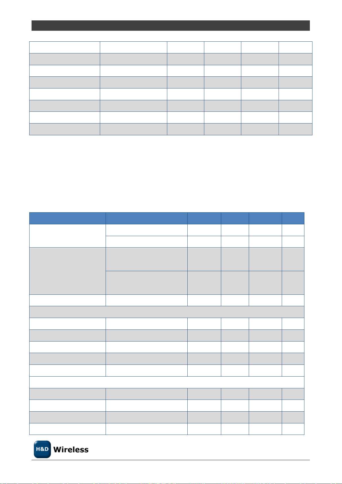
3 ELECTRICAL DATA .................................................................................................................... 7
3.1 Absolute maximum ratings ............................................................................................................................... 7
3.2 Electro Static Discharge (ESD) ......................................................................................................................... 7
3.3 Recommended operating conditions ................................................................................................................. 7
3.4 Power Consumption................................................................................................................................ .......... 7
3.5 RF Performance ................................................................................................................................................ 8
4 PIN CONFIGURATIONS........................................................................................................... 12
4.1 Pin Configuration SPB820P ............................................................................................................................12
4.2 Pin assignments ................................................................................................................................................12
5 APPLICATION INFORMATION ................................................................................................ 14
5.1 Power Supply ...................................................................................................................................................14
5.2 SHUTDOWN ...................................................................................................................................................14
5.3 Power down ......................................................................................................................................................14
5.4 Power save........................................................................................................................................................14
5.5 Initialization ................................ ..................................................................................................................... 14
5.6 Selecting UART or SPI as host interface .........................................................................................................15
5.7 UART host interface ........................................................................................................................................15
5.8 SPI host interface .............................................................................................................................................15
5.9 Interrupt Signals ..............................................................................................................................................16
5.10 RF interface .....................................................................................................................................................16
5.11 Firmware Upgrade ..........................................................................................................................................16
5.12 OTP Data .........................................................................................................................................................16
5.13 General application information .....................................................................................................................16
5.14 Typical Application ..........................................................................................................................................17
Rev. B Aug-2015 Data Sheet 1451-SPB820P page 3 (27)
Confidential
Page 4

Data Sheet 1451- Data Sheet SPB820P
5.15 oWL – Pico API ...............................................................................................................................................17
5.16 Soldering of the module ...................................................................................................................................18
6 PACKAGE SPECIFICATIONS .................................................................................................... 20
6.1 Mechanical outline of the SPB820P-xxQ module ............................................................................................20
6.2 Mounting information .....................................................................................................................................21
6.3 Markings on the SPB820P ...............................................................................................................................21
7 EVALUATION KIT ................................................................................................................... 22
7.1 Pin out for the EVK (SPB820PE) ....................................................................................................................22
8 STANDARDS COMPLIANCE .................................................................................................... 24
8.1 IEEE/IETF .......................................................................................................................................................24
8.2 WiFi Alliance ...................................................................................................................................................24
8.1 Regulatory ........................................................................................................................................................24
9 RELATED DOCUMENTS .......................................................................................................... 27
10 SALES OFFICES ....................................................................................................................... 27
Rev. B Aug-2015 Data Sheet 1451-SPB820P page 4 (27)
Confidential
Page 5
Data Sheet 1451- Data Sheet SPB820P
1 INTRODUCTION
1.1 Overview
SPB820P is a SMD module with the all the required components on a single module. It is a complete
solution designed to function as a standalone communication module, serial cable replacement or as an
easy to use WLAN addition with a minimal resource need, to an existing system.
SPB820P enables a cost efficient low power, high performance and feature rich client solution. It supports
802.11b, 802.11g and 802.11n. The SPB820P offloads the IP-stack and much of the WiFi-handling code from
the host to drastically reduce memory footprint and MCU requirements for adding WiFi to a host system.
The oWL-Pico API is simple and easy to use but still gives full detailed controlled of the WLAN.
SPB820P features an Access Point mode ideal for configuration of Wireless LAN, IP, and other system
parameters to be set by the user.
This data sheet pertains to hardware revision R2A and later of the SPB820P.
1.2 Key Features
WLAN 802.11 b/g/n radio modem for 2.4GHz ISM band.
Data Rates: 1, 2, 5.5, 6, 7.2, 9, 11, 12, 14.4, 18, 21.7, 24, 28.9, 36, 43.3, 48, 54, 57.8, 65 Mbps
Modulation: QPSK, 16QAM, 64QAM DBPSK, DQPSK, CCK, OFDM with BPSK
Open WEP, WPA/WPA2 encryption
Operates in station or access point mode
Integrated IPv4-stack
Up to four simultaneous TCP, UDP and RAW sockets.
Low power consumption
Ultra low power down mode
Simple configuration and control via oWL-Pico API.
Single Supply Voltage 2.85 – 4.35 V
Small footprint 20.9 x 26.6 mm with castellated pads.
RoHS Compliant
Integrated Chip antenna, U.FL connector or RF on pad versions available
Evaluation kits available
Rev. B Aug-2015 Data Sheet 1451-SPB820P page 5 (27)
Confidential
Page 6
Data Sheet 1451- Data Sheet SPB820P
EXAMPLE:
Product Family
SPB820
Firmware Programming
P= oWL-pico Server
Antenna Option
B=Integrated Chip Antenna
D= U.FL. RF connnector for external antenna
R= RF Pad
Operating Temperature
C= 0oC - 70oC
M= -20oC - 85oC (release pending)
Region
E= Europe and rest of the world (ETSI)
F= North America (FCC)
Package
Q= 24 pin SMD module, castellated via pads
Delivery Package
1= ESD bag
2= Tape & Reel
3= Tray
SPB820P-
BCQ1E
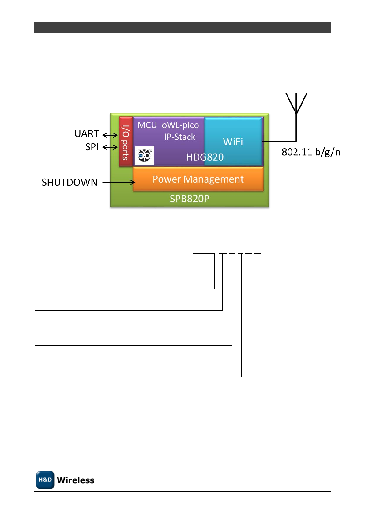
2 HARDWARE ARCHITECTURE
2.1 Block Diagram
Figure 1 Block Diagram:
2.2 Order information
Table 2.1: Ordering Information
Rev. B Aug-2015 Data Sheet 1451-SPB820P page 6 (27)
Confidential
Page 7
Data Sheet 1451- Data Sheet SPB820P
Rating
Min
Max
Unit
Supply voltage
-0.3
4.55
V
Supply voltage I/O
-0.3
3.6V and VBAT + 0.31
V
Input RF level
10
dBm
Storage temperature
-50
+125
o
C
Symbol
Min
Typ.
Max
Unit
VCC
Supply Voltage
2.85
3.3
4.35 V V
IHN
All pins
2.0 3.46
V
VIL
All pins
-0.3 0.7
V
TOP
Operating temperature SPB820P
(industrial temperature range version)
-20
+25
+85 oC
Operating temperature SPB820P
(commercial temperature range version)
01) 70 oC
Mode
Conditions
Min
Typ.
Max
Unit
Peak current
All modes
300
mA
TX [802.11b]
CCK 11Mbps
205
230
mA
TX [802.11g]
OFDM 54 Mbps
165
200
mA
TX [802.11n]
OFDM 65 Mbps
140
170
mA
3 ELECTRICAL DATA
3.1 Absolute maximum ratings
Table 3.1: Absolute maximum ratings. Exceeding any of the maximum ratings, even briefly lead to deterioration in
performance or even destruction. Values indicates condition applied one at the time.
3.2 Electro Static Discharge (ESD)
SPB820P withstands ESD voltages up to 2000V HBM (Human Body Model) according to JESD22-A114 and up
to 300 V CDV (Charged Device Model) according to JESD22-A115.
3.3 Recommended operating conditions
Table 3.2: Recommended operating conditions
1) Note: can be extended to -20
o
C, see Application Note or contact H&D Wireless
3.4 Power Consumption
If no other conditions are stated does VDD=3.6V, T
= 25oC apply.
amb
Rev. B Aug-2015 Data Sheet 1451-SPB820P page 7 (27)
Confidential
Page 8
Data Sheet 1451- Data Sheet SPB820P
RX [802.11b]
Max sensitivity
53
59
mA
RX [802.11g]
Max sensitivity
56
64
mA
RX [802.11n]
Max sensitivity
56
64
mA
Power Save1 DTIM1
Beacon Interval 100ms
2.7
mA
Power Save1 DTIM3
Beacon Interval 300ms
1.3
mA
Sleep
Between Beacons
80 uA
Shutdown2
Held in shutdown
12 uA
Power down3
PWR_DWN high
0.1 uA
Parameter
Conditions
Min
Typical
Max
Units
Frequency range
ETSI1
2412
2472
MHz
FCC1
2412
2462
Supported Channels
ETSI1
Ch.1
(2412
MHz)
Ch. 13
(2472
MHz)
FCC1
Ch.1
(2412
MHz
Ch. 11
(2462
MHz)
RF impedance
50
ohm
Transmitter performance
2,3,4
Output power, avg.
CCK 1 Mbit/s
+15
+16
+17
dBm
Output power, avg.
CCK 11 Mbit/s
+15
+16
+17
dBm
Output power, avg.
OFDM 6 Mbit/s
+13
+14
+15
dBm
Output power, avg.
OFDM 54Mbit/s
+13
+14
+15
dBm
Output power , avg.
HT20 MSC0-6
+10
+11
+12
dBm
Receiver performance 11b/g, T
amb
= 25oC
Receiver sensitivity
DSSS 1Mbit/s
-94
-87
dBm
Receiver sensitivity
DSSS 2Mbit/s
-91
-85
dBm
Receiver sensitivity
CCK 5.5Mbit/s
-89
-84
dBm
Receiver sensitivity
CCK 11Mbit/s
-86
-81
dBm
Table 3.3: Current consumption in different modes.
Notes:
1) WLAN in power save mode listening to access point beacons.
2) SHUTDOWNB pin set to low level
3) PWR_DWN pin set to high level.
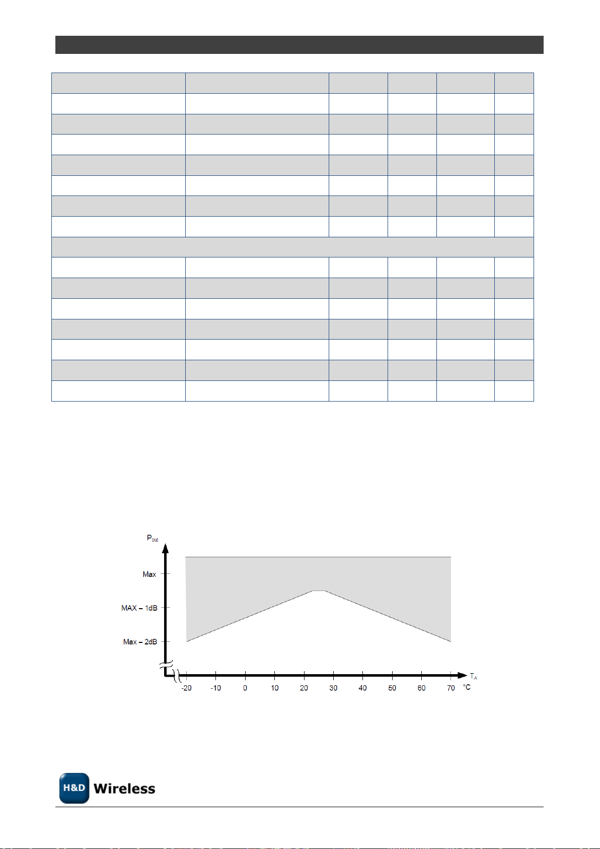
3.5 RF Performance
Conditions: VBAT= 3.6V, T
= 25°C Spectrum Mask and BER according to IEEE 802.11b/g/n specification.
amb
Rev. B Aug-2015 Data Sheet 1451-SPB820P page 8 (27)
Confidential
Page 9
Data Sheet 1451- Data Sheet SPB820P
Receiver sensitivity
BPSK 6Mbit/s
-89
-84
dBm
Receiver sensitivity
BPSK 9Mbit/s
-88
-83
dBm
Receiver sensitivity
QPSK 12Mbit/s
-86
-81
dBm
Receiver sensitivity
QPSK 18Mbit/s
-84
-79
dBm
Receiver sensitivity
16QAM 1/2 24Mbit/s
-82
-76
dBm
Receiver sensitivity
16QAM 3/4 36Mbit/s
-79
-72
dBm
Receiver sensitivity
64QAM 2/3 48Mbit/s
-74
-68
dBm
Receiver sensitivity
64QAM 3/4 54Mbit/s
-72
-67
dBm
Receiver performance 11n, T
amb
= 25
o
C
Receiver sensitivity
OFDM/BPSK 7.2Mbit/s
-90
-83
dBm
Receiver sensitivity
OFDM/BPSK 14.4Mbit/s
-88
-80
dBm
Receiver sensitivity
OFDM/BPSK 21.7Mbit/s
-86
-78
dBm
Receiver sensitivity
OFDM/16-QAM 28.9Mbit/s
-83
-75
dBm
Receiver sensitivity
OFDM/16-QAM 43.4Mbit/s
-79
-71
dBm
Receiver sensitivity
OFDM/64-QAM 57.8Mbit/s
-72
-67
dBm
Receiver sensitivity
OFDM/64-QAM 65Mbit/s
-70
-66
dBm
Table 3.4: RF performance.
1) SPB820P products sold for final use in North America has the Operations Region set to FCC in
the OTP memory. This limits the use of frequencies to those allowed in FCC Part15.
2) TX output power is noted as average power. Peak power may be 2-5 dBm higher for DSSS
modulation and 6-10 dBm for OFDM.
3) TX output power varies with temperature as shown in Figure 2
Figure 2: Pout vs ambient temperature
4) TX Output power varies with temperature as shown in Figure 3
Rev. B Aug-2015 Data Sheet 1451-SPB820P page 9 (27)
Confidential
Page 10

Data Sheet 1451- Data Sheet SPB820P
Parameter
Symbol
Min
Max
ns
Comments
Input set-up time
tISU
5 ns
Input hold time
tIH
5 ns
Clock fall time
tTHL
10
ns
Clock rise time
tTLH
10
ns Output delay time
tODLY
0
14
ns
Clock Frequency
25
MHz
Figure 3: Output Power vs. VCC voltage
3.5.1 SPI timing characteristics
The SPI host interface timing is showed in Figure 3-4 and Table 3-5
Condition: VDDIO= 1.7 – 3.6 V, Tamb= 0 to +70°C Parameter Condition Min Typical Max Units
Figure 3-4: SPI timing diagram (default mode
Rev. B Aug-2015 Data Sheet 1451-SPB820P page 10 (27)
Confidential
Page 11

Data Sheet 1451- Data Sheet SPB820P
Parameter
Symbol
Min
Typ
Max
Units
Comments
Input low voltage
VIL
-0.3
0.3*VIO V
Input high voltage
VIH
0.625*VIO
VIO+0.3 V
Input leakage current
IIL
-1 1
μA
Output low voltage
VOL
0.4
V
Iout<1mA
Output high voltage
VOH
VIO-0.4 V Iout>-1mA
Input pin capacitance
CIP
5.5 pF VDDIO, VDD_SDIO
VIO
1.7 3.6 V
Table 3-5: SPI timing parameter values
3.5.2 Digital input/output pad (I/O)
The digital I/O pads are of type none inverting three-state driver/receiver. The I/O pin functional schematic
is shown in Figure 3-5. It includes an input buffer and an output buffer with enable/disable control inputs. It
also includes a hold-function. When an I/O is neither driven by the internal nor by an external circuitry, the
hold function holds the latest state of the I/O. This is the case for example when Shutdown is active.
Figure 3-5: Function schematics of the I/O input pad configuration.
Table 3-6: I/O pin DC characteristics.
3.5.3 Protection of digital pins
All digital pins are protected against over-voltage with a “snap-back” circuit connected between the pad
and GND. The “snap-back” voltage is 6.2 V and the holding voltage is 6 V. This provides a satisfying
protection against over voltages and ESD. Also there is a diode included to protect against reversed
voltages.
Rev. B Aug-2015 Data Sheet 1451-SPB820P page 11 (27)
Confidential
Page 12

Data Sheet 1451- Data Sheet SPB820P
Pin
Function
Type
Description 1 VDD
S
Supply pin 3.3V
2
JTAG_TMS
I/O
Production Test interface, Do Not Connect
3
JTAG_TCK
I
Production Test interface, Do Not Connect
4
SPI_MOSI
I
SPI Host interface Input
5
SPI_CLK
I
SPI Host interface Input
6
UARTb_SPI
WAKE_UP
I
Pin Sensed at boot to select UART or SPI Host Interface
After boot use to wake up the SPB820P from sleep
mode 7 JTAG_TDI
NC
Production Test interface, Do Not Connect
8
JTAG_TDO
NC
Production Test interface, Do Not Connect
4 PIN CONFIGURATIONS
4.1 Pin Configuration SPB820P
Figure 4.1: Package pin out, top view
4.2 Pin assignments
Rev. B Aug-2015 Data Sheet 1451-SPB820P page 12 (27)
Confidential
Page 13

Data Sheet 1451- Data Sheet SPB820P
9
UART_RX/SPI_MISO
I/O
UART Host interface Receive
SPI Host Interface Output
10
UART_TX/SPI_CS
O
UART Host Interface Transmit
SPI Host Interface Chip Select
11
UART_CTS/SPI_INT
I
UART Host Interface CTS
SPI Host Interface Interrupt
12
UART_RTS
O
UART Host Interface RTS
13
GND
S
Ground
14
RF_PAD
Input
RF Signal (only for –R version)
15
GND
S
Ground
16
LED1
Output
LED1 Indicates WLAN association1
17
GPIO2
NC
GPIO pin, function defined by FW can be left
unconnected
18
HOST_ATT
Output
Wake Host From SPB820P
19
GPIO3
NC
GPIO pin, function defined by FW can be left
unconnected
20
GPIO4
NC
GPIO pin, function defined by FW can be left
unconnected
21
GPIO1
NC
GPIO pin, function defined by FW can be left
unconnected
22
SHUTDOWNb
Input
Module Reset Signal, Internal Pull up, not required to
be connected.
23
GPIO6
Input
GPIO pin, function defined by FW can be left
unconnected
24
PWR_OFF
Input
Active high powers down the SPB820P, Internal Pull
Down
Table 4.1: Pin Description for SPB820P R2A
1: Depends on firmware.
Rev. B Aug-2015 Data Sheet 1451-SPB820P page 13 (27)
Confidential
Page 14

Data Sheet 1451- Data Sheet SPB820P
5 APPLICATION INFORMATION
5.1 Power Supply
SPB820P should be powered by a single supply voltage on the supply on VDD, pin 1. The SPB820P generates
all required voltages on board.
5.2 SHUTDOWN
The SHUTDOWNb pin shall be set high during normal operation. Pulling the SHUTDOWNb pin low, sets the
HDG820 in reset mode. This turns OFF most parts of the circuit and minimizes the current consumption. All
I/O interface pins are set to predefined states (high, low or high-z) when in Shutdown mode. For minimum
power consumption turn external 1.5 V, OFF while the SHUTDOWNb pin is low.
To end reset mode set SHUTDOWNb pin high wait for the HDG820 to signal that it is ready with a low pulse
on HOST_ATT, or wait t
On SPB820P SHUTDOWNb has an internal delay circuit that will pull SHUTDOWNb high, 100 ms after
voltage is applied on VDD or PWR_DWN is released. If not used by the host the pin can be left
unconnected.
for it to respond on the host interface.
READY
5.3 Power down
By raising the PWR_DWN signal high the supply voltage to the SPB820P is switch off by the on board PMOS
FET transistor and the current consumption is brought to a minimum.
5.4 Power save
Power save is an energy saving mode where HDG820 is only listening at regular intervals for the beacons
transmitted from an access point and is set in sleep mode in between. During this sleep mode, FW is kept in
RAM but all not needed functions are turned off. Since the receive time is very short compared to the
listening interval the average current consumption is reduced significantly.
The timing of the listening interval is based on the internal 32 kHz clock.
5.5 Initialization
At power on and after reset the SPB820P will load firmware and calibrate the radio. During these 5s the
upgrade mode can be entered by the host or a serial port terminal. The UARTb_SPI signal will be sampled
at the end of the initialization period.
Rev. B Aug-2015 Data Sheet 1451-SPB820P page 14 (27)
Confidential
Page 15

Data Sheet 1451- Data Sheet SPB820P
H
L
H
L
H
L
PWR_DWN (input)
VDD (supply)
SHUTDOWN (input)
HOST_ATT (output)
UARTb_SPI (input)
t
VDD_ON
t
SHUTDOWN
t
READY
H
L
UARTb_SPI (pull-down)
WAKE_UP(pull-up)High: SPI
Low: UART
H
L
t
PWR_DWN
Parameter
Symbol
Min
Typ
Max
Unit
Comment
VDD rise time
t
VDD_ON
2
μs PWR_DWN release to VDD high
t
PWR_DWN
150 μs
SHUTDOWNb release delay
t
SHUTDOWN
1
100*
ms
Internal RC
link delay
IO supply ramp time
t
VDD_LDO_IO
360
μs Digital 1.5V supply ramp time
t
VDD_DCDC
150
μs SHUTDOWNb release to host alert
t
READY
4
s
Figure 6; Initialization timing
Table 7: Initialization timing
5.6 Selecting UART or SPI as host interface
By setting UARTb_SPI low or high during the initialization the type of host interface can be selected.
If UARTb_SPI is set low UART will be selected as host interface
If UARTb_SPI is set high SPI will be selected as host interface.
Note that the UARTb_SPI is sampled every time the SPB820P initializes, at power on and after PWR_DWN
or SHUTDOWNB signals are released.
After initialization the UARTb_SPI pin switch function to WAKE_UP.
5.7 UART host interface
If UARTb_SPI is low during initialization of the SPB820P the UART1_TX and UART1_RX will become the host
interface of the SPB820P
To communicate with the SPB820P an UART interface is used. The signals “UART1_RTS” and “UART1_CTS”
are only active when hardware flow control is enabled by commands from the host.
The SPB820P supports baud rates from 9600 baud up to 4 000 000 baud on the UART interface.
5.8 SPI host interface
If UARTb_SPI is high during initialization of the SPB820P will use the SPI bus in slave mode as host interface.
The SPI interface support a maximum clock rate of 25MHz
Note: SPI host interface is only supported for oWL-pico Server FW release 2.2 and higher.
Rev. B Aug-2015 Data Sheet 1451-SPB820P page 15 (27)
Confidential
Page 16

Data Sheet 1451- Data Sheet SPB820P
5.9 Interrupt Signals
5.9.1 WAKE_UP
After initialization the UARTb_SPI signal assumes the function of WAKE_UP.
Active low input signal, allows the host to wake up the SPB820P from Power Save, if not utilized it can be
left unconnected as the signal has an internal pull up resistor.
5.9.2 HOST_ATT
Active low output signal. Allows the host to go into low power mode and be woken by the SPB820P when
data is received on the WLAN.
HOST_ATT signals with a low pulse when the HDG820 is ready after power on.
5.10 RF interface
The SPB820P-Bxx has a high performance chip antenna as the primary RF interface.
The SPB820P-Dxx has a U.FL connector as RF interface. Use Hirose U.FL receptacle or comparable for
connection.
The SPB820P-Rxx has a pad 14 as RF interface.
5.11 Firmware Upgrade
The firmware in SPB820P can be upgraded either via the serial port or over the air. Upgrade over the serial
port has to be initiated by the host or via serial port terminal during start up. Upgrade over the air is
initialized by the host via oWL-pico command. Always check the compatibility of the FW version and HW
version of your device before attempting an upgrade. Upgrades will not overwrite data stored in the OTP
memory.
The SPB820P is an 802.11 compliant WLAN device functional within the ISM band on 2.4GHz using BPSK,
QPSK, 16-QAM and 64-QAM modulations with a calibrated fixed value for maximum transmission output
power. These properties are an integral part of the device and cannot be modified or customized by change
of firmware or other alterations.
5.12 OTP Data
MAC address, calibration data and region of intended use, is permanently stored in One Time
Programmable register during production and cannot be altered by any command or re-programming. A
firmware upgrade will not affect OTP data.
5.13 General application information
5.13.1 Design directions
The design using the SPB820P must be performed according to good RF design considerations. Keep the
area under the antenna free from all metal including signal or ground wires.
Rev. B Aug-2015 Data Sheet 1451-SPB820P page 16 (27)
Confidential
Page 17

Data Sheet 1451- Data Sheet SPB820P
5.14 Typical Application
Figure 7: Typical application connection with UART host interface
Figure 8: Typical application connection with SPI host interface
5.15 oWL – Pico API
The HDG820/SPB820P utilizes the oWL-pico API for communication from and to the host processor.
This gives the host control over the WLAN interface and the possibility to set up up to 4 simultaneous TCP,
RCP or RAW sockets. All IP and WLAN protocols are offloaded from the host. See Figure 9
Rev. B Aug-2015 Data Sheet 1451-SPB820P page 17 (27)
Confidential
Page 18

Data Sheet 1451- Data Sheet SPB820P
Figure 9: oWL-pico API
Please refer to http://pico.hd-wireless.se for more information in the oWL-pico API and reference designs.
5.16 Soldering of the module
The SPB820P is a surface mount PCB module. If the modules has been exposed to air or are delivered in
non-hermetically sealed packages it is recommended to bake the modules before soldering. To lower the
moisture content bake the packages for 192 hours at 40–45°C and <5%RH, or 24 hours at 120–130°C,
depending on the maximum temperature rating of the packaging. The recommended solder profile is
pictured in Figure 5.6
Rev. B Aug-2015 Data Sheet 1451-SPB820P page 18 (27)
Confidential
Page 19

Data Sheet 1451- Data Sheet SPB820P
Type
Rising Zone
Preheat
Zone
Reflow
Zone
Peak
Zone
Cooldown
Zone
Comment
PSR
125ºC-Peak
No
110190ºC
60-120 s
>220ºC
>30 s
230250ºC
Peak125ºC
No
Figure 5.6: Reflow Temperture Profile.
5.16.1 Environmental statement
The SPB820P is designed and manufactured to comply with the RoHS and Green directives.
Rev. B Aug-2015 Data Sheet 1451-SPB820P page 19 (27)
Confidential
Page 20

Data Sheet 1451- Data Sheet SPB820P
6 PACKAGE SPECIFICATIONS
6.1 Mechanical outline of the SPB820P-xxQ module
Figure 10: Top view
Figure 11: Side View
Rev. B Aug-2015 Data Sheet 1451-SPB820P page 20 (27)
Confidential
Page 21

Data Sheet 1451- Data Sheet SPB820P
6.2 Mounting information
6.2.1 Recommended land pattern on the PCB for SPB820P-xxQ
Figure 12: SPB820P-xxQ land pattern
Place no via holes or exposed metal under the module.
For the SPB820P-B with chip antenna an area around the module should be kept free of metal in all layers
of the PCB, see Figure 12.
6.3 Markings on the SPB820P
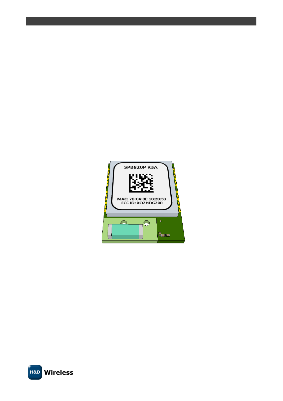
The label on the EMC Shield is imprinted with the FCC ID and serial number.
Rev. B Aug-2015 Data Sheet 1451-SPB820P page 21 (27)
Confidential
Page 22

Data Sheet 1451- Data Sheet SPB820P
Header Pin
Pin Function
SPB820P-xxP
Pad
Comment
1
UART_RTS
12
Optional
2
PWR_DWN
24
Internal pull down can be left
unconnected
3
UART_TX
10
To host RX
4
UART_RX
9
To host TX
5
UART_CTS
11
Optional
6
HOST_ATT
18
Optional Host attention to wake up
the host from sleep.
7
WAKE_UP
23
Optional to wake up SPB820P from
sleep.
8
NC
Do not connect
9
Ground
13, 15
10
Supply 3.3V
1
7 Evaluation Kit
The Evaluation kit has the main signals of the SPB820P conveniently available on a 10 position header
socket. The LED indicator signal is connected to an onboard LED. As the PWR_DWN signal has an onboard
pull down resistor that will keep it low (active) it can be left unconnected. To power down the SPB820P the
PWR_DWN signal has to be set high.
7.1 Pin out for the EVK (SPB820PE)
Figure 13: SPB820P EVK pins top view
Rev. B Aug-2015 Data Sheet 1451-SPB820P page 22 (27)
Confidential
Page 23

Data Sheet 1451- Data Sheet SPB820P
Table 7.1: SPB820P Evaluation Kit pin out
To connect to a host MCU in UART mode follow the block diagram below:
Rev. B Aug-2015 Data Sheet 1451-SPB820P page 23 (27)
Confidential
Page 24

Data Sheet 1451- Data Sheet SPB820P
Standard
Notes
802.11b
Rates: 1, 2, 5.5, 11 Mbps
802.11d
International (country-to-country) roaming extensions
802.11g
Rates: 6, 9, 12, 18, 24, 36, 48, 54 Mbps
802.11i
Enhanced security
802.11j
Extensions for Japan
802.11n
Rates: 7.2, 14.4, 21.7, 28.9, 43.3, 57.8, 65
Specification
Notes
WiFi 802.11n STA
WPS2.0
Country
Approval
authority
Regulatory
Frequency band
USA
FCC
FCC ID: XO2HDG200
2.412 GHz -2.462 GHz
Canada
IC
RSS: TBA
2.412 GHz -2.462 GHz
Europe
National
ETSI
2.412 GHz -2.4835 GHz
8 STANDARDS COMPLIANCE
8.1 IEEE/IETF
Table 8.1: Applicable IEEE standards
8.2 WiFi Alliance
Table 8.2: Applicable WiFi Alliance standards
8.1 Regulatory
Table 8.3: Regulatory standards
8.1.1 FCC (United States of America)
This equipment complies with Part 15 of the FCC rules and regulations.
To fulfill FCC Certification requirements, an OEM manufacturer must comply with the following regulations:
The modular transmitter is labeled with its own FCC ID number, and, if the FCC ID is not visible when the
module is installed inside another device, then the outside of the device into which the module is installed
must also display a label referring to the enclosed module. This exterior label can use wording such as the
following:
Rev. B Aug-2015 Data Sheet 1451-SPB820P page 24 (27)
Confidential
Page 25

Data Sheet 1451- Data Sheet SPB820P
Example of label required for OEM product containing SPB820P module
NOTE: Only antennas approved may be used with SPB820 module. The SPB820 Module may be integrated
with custom design antennas which OEM installer must authorize following the FCC 15.201 requirements
IMPORTANT: This equipment complies with Part 15 of the FCC Rules. Operation is subject to the following
two conditions: (1) this device may not cause harmful interference, and (2) this device must accept any
interference received, including interference that may cause undesired operation (FCC 15.19).
The internal / external antenna(s) used for this mobile transmitter must provide a separation distance of at
least 20 cm from all persons and must not be co-located or operating in conjunction with any other
antenna or transmitter.
This device is approved as a mobile device with respect to RF exposure compliance, and may only be
marketed to OEM installers. Use in portable exposure conditions (FCC 2.1093) requires separate equipment
authorization.
IMPORTANT: Modifications not expressly approved by this company could void the user's authority to
operate this equipment (FCC section 15.21).
IMPORTANT: The finished product is required to comply with all applicable FCC equipment authorizations
regulations, requirements and equipment functions not associated with the transmitter module portion.
Compliance for unintentional radiators (Part 15 Subpart B “Unintentional Radiators”), such as digital
devices, computer peripherals, radio receivers, etc. has to be demonstrated.
8.1.2 IC (Canada)
Equipment is subject to certification under the applicable RSSs, shall be permanently labeled on each item,
or as an inseparable combination. The label must contain the following information for full compliance:
IMPORTANT: This equipment for which a certificate has been issued is not considered certified if it is not
properly labeled. The information on the Canadian label can be combined with the manufacturer's other
labeling requirements
IMPORTANT: Operation is subject to the following two conditions: (1) this device may not cause harmful
interference, and (2) this device must accept any interference received, including interference that may
cause undesired operation.
Rev. B Aug-2015 Data Sheet 1451-SPB820P page 25 (27)
Confidential
Page 26

Data Sheet 1451- Data Sheet SPB820P
IMPORTANT: To reduce potential radio interference to other users, the antenna type and its gain should be
so chosen that the equivalent isotropically radiated power (e.i.r.p.) is not more than that permitted for
successful communication.
IMPORTANT: The installer of this radio equipment must ensure that the antenna is located or pointed such
that it does not emit RF field in excess of Health Canada limits for the general population. Consult Safety
Code 6, obtainable from Health Canada's website www.hc-sc.gc.ca/rpb.
8.1.3 ETSI (Europe)
The SPB820P module has been certified for use in European union countries according to ETSI EN 300 328
(Electromagnetic compatibility and Radio spectrum matters for equipment operating in the 2,4 GHz ISM
band using spread spectrum modulation techniques). This standard is harmonized within the European
Union and covering essential requirements under article 3.2 of the R&TTE-directive.
If the SPB820P module are incorporated into a product, the manufacturer must ensure compliance of the
final end-user product to the European harmonized EMC and low voltage/safety standards. A declaration of
conformity must be issued for the product including compliance references to these standards. Underlying
the declaration of conformity a technical construction file (TCF), including all relevant test reports and
technical documentation, must be issued and kept on file as described in Annex II of the R&TTE-directive.
Furthermore, the manufacturer must maintain a copy of the SPB820P module documentation and ensure
the final product does not exceed the specified power ratings, antenna specifications, and/or installation
requirements as specified in the user manual. If any of these specifications are exceeded in the final
product, a complete re-test must be made in order to comply with all relevant standards as basis for CEmarking. A submission to notified body must be used only if deviations from standards have been found or
if non-harmonized standards have been used.
Rev. B Aug-2015 Data Sheet 1451-SPB820P page 26 (27)
Confidential
Page 27

Data Sheet 1451- Data Sheet SPB820P
9 Related Documents
oWL-pico Doxygen information in oWL-pico Software Framework
1543-SPB820P (o)WL-pico API, user manual
1453-SPB820P Power Management Application Note
Wiki at http://pico.hd-wireless.se
10 SALES OFFICES
Global Sales Office Sweden
H&D Wireless AB
H&D Wireless AB
Norgegatan 1
164 32 Kista
Sweden
E-mail: info@hd-wireless.se
Support: support@hd-wireless.se
Home page: www.hd-wireless.se
Local sales offices and representatives see www.hd-wireless.se
Rev. B Aug-2015 Data Sheet 1451-SPB820P page 27 (27)
Confidential
 Loading...