HANBit HMN1288J Service Manual

查询HMN1288J供应商
HANBit
GENERAL DESCRIPTION
The HMN1288J Nonvolatile SRAM is a 1,048,576-bit static RAM organized as 131,072 bytes by 8 bits.
The HMN1288J has a self-contained lithium energy source provide reliable non-volatility coupled with the unlimited write
cycles of standard SRAM and integral control circuitry which constantly monitors the single 5V supply for an out-of-
tolerance condition. When such a condition occurs, the lithium energy source is automatically switched on to sustain the
memory until after Vcc returns valid and write protection is unconditionally enabled to prevent garbled data. In addition the
SRAM is unconditionally write-protected to prevent an inadvertent write operation. At this time the integral energy source is
switched on to sustain the memory until after VCC returns valid.
The HMN1288J uses extremely low standby current CMOS SRAM’s, coupled with small lithium coin cells to provide non-
volatility without long write-cycle times and the write-cycle limitations associated with EEPROM.
FEATURES
w Access time : 55, 70 ns
w High-density design : 4Mbit Design
w Battery internally isolated until power is applied
w Industry-standard 34-pin 128K x 8 pinout
w Unlimited write cycles
w Data retention in the absence of VCC
w 10-years minimum data retention in absence of power
w Automatic write-protection during power-up/power-down
cycles
w Data is automatically protected during power loss
w Conventional SRAM operation; unlimited write cycles
Non-Volatile SRAM MODULE 1Mbit (128K x 8-Bit),34Pin-JLCC, 5V
PIN ASSIGNMENT
/WE
/OE
/CE
D(7)
D(6)
D(5)
D(4)
D(3)
D(2)
D(1)
D(0)
1
2
4
5
6
7
8
9
10
11
12
13
14
15
16
17
/NBW
A(16)
/RST
VCC
VSS
JLCC
TOP VIEW
HMN1288J
Part No. HMN1288J
34
NC
33
NCA(15)
323
A(14)
31
A(13)
30
A(12)
29
A(11)
28
A(10)
27
A(9)
26
A(8)
25
A(7)
24
A(6)
23
A(5)
22
A(4)
21
A(3)
20
A(2)
19
A(1)
18
A(0)
OPTIONS MARKING
w Timing
55 ns -55
70 ns -70
URL: www.hbe.co.kr 1 HANBit Electronics Co.,Ltd.
Rev.0.0 (FEBRUARY/ 2002)

HANBit
HMN1288J
FUNCTIONAL DESCRIPTION
The HMN1288J executes a read cycle whenever /WE is inactive(high) and /CE is active(low). The address specified by
the address inputs(A0-A16) defines which of the 131,072 bytes of data is accessed. Valid data will be available to the eight
data output drivers within t
When power is valid, the HMN1288J operates as a standard CMOS SRAM. During power-down and power-up cycles, the
HMN1288J acts as a nonvolatile memory, automatically protecting and preserving the memory contents.
The HMN1288J is in the write mode whenever the /WE and /CE signals are in the active (low) state after address inputs
are stable. The later occurring falling edge of /CE or /WE will determine the start of the write cycle. The write cycle is
terminated by the earlier rising edge of /CE or /WE. All address inputs must be kept valid throughout the write cycle. /WE
must return to the high state for a minimum recovery time (tWR) before another cycle can be initiated. The /OE control
signal should be kept inactive (high) during write cycles to avoid bus contention. However, if the output bus been enabled
(/CE and /OE active) then /WE will disable the outputs in t
The HMN1288J provides full functional capability for Vcc greater than 4.75 V and write protects by 4.5 V nominal. Power-
down/power-up control circuitry constantly monitors the Vcc supply for a power-fail-detect threshold V
below the V
all outputs are high impedance. As Vcc falls below approximately 2.7 V, the power switching circuit connects the lithium
energy soure to RAM to retain data. During power-up, when Vcc rises above approximately 2.7 volts, the power switching
circuit connects external Vcc to the RAM and disconnects the lithium energy source. Normal RAM operation can resume
after Vcc exceeds 4.75 volts.
threshold, the SRAM automatically write-protects the data. All inputs to the RAM become “ don’t care” and
PFD
(access time) after the last address input signal is stable.
ACC
from its falling edge.
ODW
. When VCC falls
PFD
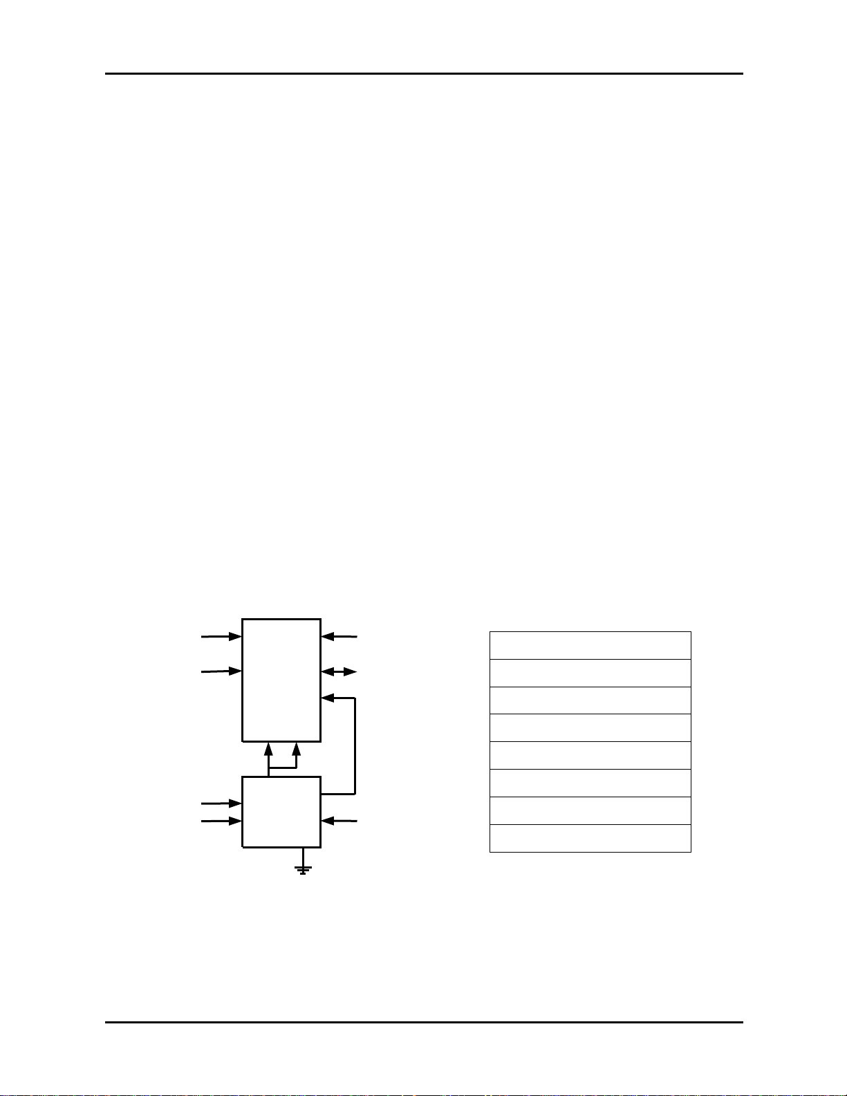
BLOCK DIAGRAM PIN DESCRIPTION
/OE
/WE
/CE1
/CE2
Vcc
Vout
/CE
/RESET
A(0:16)
DQ(0:7)
/CE_con
Vcc
A0-A16 : Address Input
/CE : Chip Enable
VSS : Ground
DQ0-DQ7 : Data In / Data Out
/WE : Write Enable
/OE : Output Enable
VCC: Power (+5V)
NC : No Connection
URL: www.hbe.co.kr 2 HANBit Electronics Co.,Ltd.
Rev.0.0 (FEBRUARY/ 2002)

HANBit
HMN1288J
TRUTH TABLE
MODE /OE /CE /WE I/O OPERATION POWER
Not selected X H X High Z Standby
Output disable H L H High Z Active
Read L L H D
Write X L L DIN Active
Active
OUT
ABSOLUTE MAXIMUM RATINGS
PARAMETER SYMBOL RATING CONDITIONS
DC voltage applied on V
DC Voltage applied on any pin excluding VCC relative
to VSS
Operating temperature T
Storage temperature T
Soldering temperature T
NOTE:
Functional operation should be restricted to the Recommended DC Operating Conditions detailed in this data sheet.
Exposure to higher than recommended voltage for extended periods of time could affect device reliability.
Permanent device damage may occur if Absolute Maximum Ratings are exceeded.
RECOMMENDED DC OPERATING CONDITIONS ( TA= T
PARAMETER SYMBOL MIN TYPICAL MAX
Supply Voltage VCC 4.5V - 5.5V
Ground VSS 0 0 0
Input high voltage VIH 2.0 - V
Input low voltage
relative to VSS VCC -0.3V to 7.0
CC
VT -0.3V to Vcc+0.3
OPR
STG
SOLDER
VIL -0.3 - 0.8V
0 to 70°C
-55°C to 125°C
260°C
)
OPR
For 10 second
V
T
VCC+0.3
≤
0.3
CC+
Typical values indicate operation at TA = 25℃
NOTE:
CAPACITANCE (TA=25℃, f=1MHz, VCC=5V)
DESCRIPTION CONDITIONS SYMBOL MAX MIN UNIT
Input Capacitance Input voltage = 0V CIN 8 - pF
Input/Output Capacitance Output voltage = 0V C
URL: www.hbe.co.kr 3 HANBit Electronics Co.,Ltd.
Rev.0.0 (FEBRUARY/ 2002)
10 - pF
I/O
 Loading...