

HANBit HFDOM40S3Rxxx Service Manual

HANBit HFDOM40S3Rxxx
40Pin Flash Disk Module Min.16MB ~ Max.512MB,
True IDE Interface
1. PRODUCT OVERVIEW
GENERAL DESCRIPTION
The HFDOM40S3Rxxx series 40Pin Flash Disk Module is a flash technology based with True IDE interface flash
memory card. It is constructed with flash disk controller chip and NAND-type (Samsung) flash memory device. The
HFDOM40S3R-xxx series operates in both 3.3-Volt and 5.0-Volt power supplies. It comes in capacity of 16, 32, 48, 64, 80,
96, 128, 144, 160, 192,
By optimizing flash memory management, the life of this HFDOM40S3Rxxx series can be extended to its maximum level.
Because the ECC function is included, the correctness of data transfer between the HFDOM40S3Rxxx series and a True
IDE compatible interface device can be guaranteed.
The HFDOM40S3Rxxx series is fully compatible with applications such as CPU card / board, set top box, industry /
military PC / Notebook, security equipment, measuring instrument and embedded systems.
FEATURES
- ATA / True IDE compatible host interface
- ATA command set compatible
- Automatic sensing of PC Card ATA or true IDE host interface.
- Very high performance, very low power consumption
- Automatic error correction
- Auto Standby to save power consumption.
- Supports power down commands and sleep modes.
- Integrated PCMCIA attribute memory of 256 bytes (CIS)
- Support for 8 or 16 bit host transfers
- 3.3V/5.0V operation voltage
- Host Interface bus width : 8/16 bit Access
- Flash Interface bus width : 8 bit Access
- Capacity : Min. 16MB ~ Max. 512MB
- MTBF > 1,000,000 hours.
- Minimum 10,000 insertions.
- Shock : 2,000 G max.
- Vibration : 15 G peak to peak max.
PRODUCT SPECIFICATIONS
208, 224, 256, 272,288, 320, 384 and up to 512MByte formatted 40Pin type .
Capacities :
16, 32, 48, 64, 80, 96, 128, 144, 160, 192, 208, 224, 256, 272,288, 320, 384 and up to 512MB (formatted)
System Compatibility :
Please refer to the compatibility list of index.
Performance :
Host Data Transfer Rates : up to 16.6 MB/sec, PIO mode 4; 16.6MB/sec
URL:www.hbe.co.kr 1 / 31 HANBit Electronics Co., Ltd.
Rev. 1.0 (October, 2004)
HANBit HFDOM40S3Rxxx
Operating Voltage : 3.3V / 5.0V 10%
Power consumption : 3.3V ± 5%
Read mode <30 mA
Write mode <56 mA
Stop mode <2 mA
Environment conditions :
Operating temperature 0°C to + 70°C
Storage temperature - °C to + °C
Relative humidity
ELECTRICAL SPECIFICATIONS
Table 1.1 Absolute Maximum Ratings
Symbol Parameter Rating Units
VDD Power supply -0.3 to 6.0 V
VIN Input voltage -0.3 to VDD+0.3 V
V
Output voltage -0.3 to VDD+0.3 V
OUT
T
Storage temperature
STG
8% to 95%, non-condensing
-55 to 150
o
C
Table 1.2 Recommended Operating Conditions
Symbol Parameter Min. Max. Units
VDD Power supply 3.0 3.6 V
VIN Input voltage
T
Operating temperature 0 70
OPR
-0.3
Table 1.3 DC Characteristics
Sym. Parameter Min Typ Max Units
VIL Input low voltage 0.3V
VIH Input high voltage 0.7V
VIL Schmitt input low voltage 1.22 V
VIH Schmitt input high voltage 2.08 V
VOL Output low voltage 0.4 V
VOH Output high voltage 2.3 1 V
RI Input pull up/down resistance 75
+0.3 V
V
DD
DD
V
DD
o
C
V
kΩ
URL:www.hbe.co.kr 2 / 31 HANBit Electronics Co., Ltd.
Rev. 1.0 (October, 2004)
HANBit HFDOM40S3Rxxx
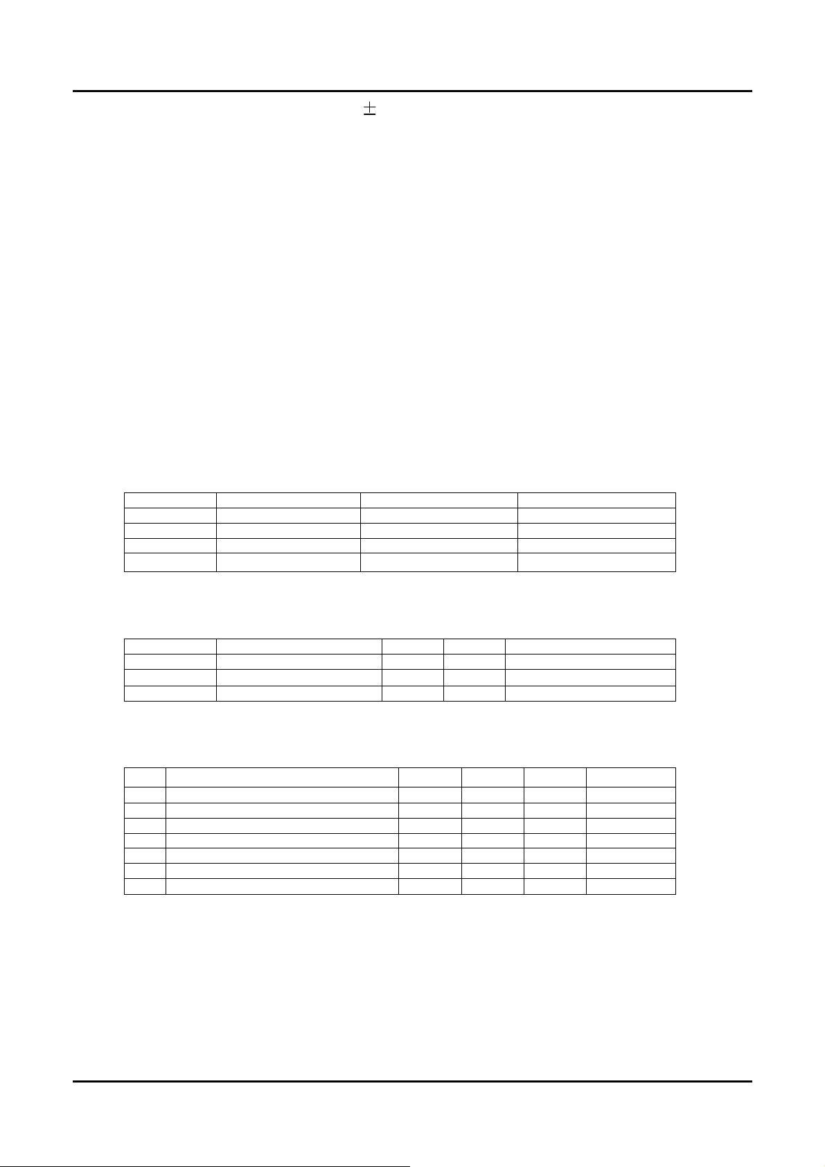
PHYSYCAL SPECIFICATION
TOP Side
123
Bottom Side
40
39
TOP Side
Bottom Side
Top-Connector
Attach
2
1
1
2
39
40
TOP Side
Bottom Side
Bottom-Connector
Attach
55.50±0.1mm
Jumper
Master Slave
2,3
Close
40
1,2
Close
30.50±0.2mm
23
1
2
39
8.90mm±0.1mm
1
7.50mm
1.4mm±0.1mm
URL:www.hbe.co.kr 3 / 31 HANBit Electronics Co., Ltd.
Rev. 1.0 (October, 2004)
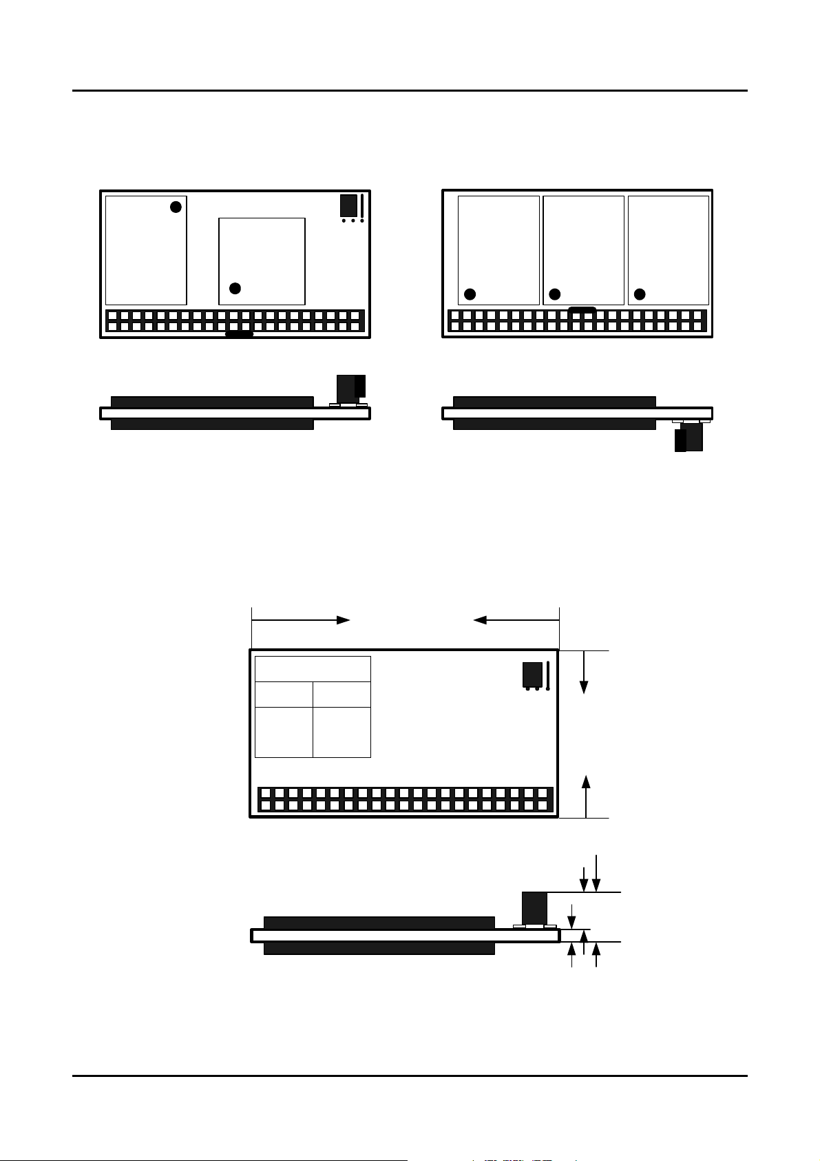
HANBit HFDOM40S3Rxxx
3.8±0.1mm
2.54±0.05mm
6.0±0.1mm
2.54±0.05mm
48.20±0.1mm
55.30±0.1mm
< View from connector side >
Figure 1.0 40 pin Type Flash Disk Module Dimensions
URL:www.hbe.co.kr 4 / 31 HANBit Electronics Co., Ltd.
Rev. 1.0 (October, 2004)

HANBit HFDOM40S3Rxxx
INSTALLTION GUIDE
1) Setting Method
① Make sure your computer is turned off before you open the case.
② Plug the carefully into the 40pin IDE slot on your computer.
Caution: Make sure to align pin1 on host adapter interface connector with pin 1 on your Flash Disk Module. Pin 1
is indicated by a triangle on the Flash Disk Module connector.
③ The Flash Disk Module is used power connector cable of the computer.
Caution: If you need to remove your Flash Disk Module, use both hands to pull it out carefully.
④ Check all cable connections and then replace your computer cover.
2) BIOS setting Method
Before you format or partition your new drive, you must configure your computer's BIOS so that the computer can
recognize your new drive.
① Turn your computer on. As your computer start up, watch the screen for a message describing how to run the
system setup program on the screen (sometimes called BIOS or CMOS setup). This is usually done by pressing a
special key, such as Delete, Esc or F1 during startup. See your computer manual for details. Press the appropriate
key to run the system setup program.
② If your BIOS provides automatic drive detection (an "AUTO" drive type), select this option. ( We
recommend to use Normal / CHS mode to partition your Flash Disk Module to get the maximum formatted
capacity. )
This allows your computer to configure itself automatically for your new drive.
If your BIOS dose not provide “AUTO” drive detection, select "User-defined" drive setting and enter the
CHS values from the table. BIOS Settings (see specification) Capacity Cylinders Heads Sectors(unformatted)
③ Save the settings and exit the System Setup program. ( your computer will automatically reboot ) After you
configure your computer, you can use the standard DOS commands to partition and format your Flash Disk Module,
as described below.
3) Formatting Method
To partition your new Flash Disk Module with Microsoft DOS program :
① Insert a bootable DOS diskette into your diskette drive and restart your computer.
② Insert a DOS program diskette that contains the FDISK.EXE and FORMAT.COM
programs into your diskette drive. Use the same DOS version that is on your bootable diskette. At the A:\ > prompt,
type “FDISK” and press Enter.
③ Select “Create DOS partition or logical DOS drive” by pressing 1. Then press Enter.
④ Select “Create primary DOS partition” by pressing 1 again. Then press Enter.
Create your first drive partition. If you are creating a partition that will be used to boot your computer (drive C),
make sure that the partition is marked active.
⑤ Create an extended partition and additional logical drives as necessary, until all the space on your new hard drive
has been partitioned.
⑥ When the partitioning is complete, FDISK reboots your computer.
Caution: Make sure to use the correct drive letters so that you do not format a drive that already contains data.
⑦ At the A:\ > prompt, type “format c:/s”, where c is the letter of your first new partition, Repeat the format process
for all the new partitions you have created.
⑧ After you format your drive, it is ready to use.
URL:www.hbe.co.kr 5 / 31 HANBit Electronics Co., Ltd.
Rev. 1.0 (October, 2004)

HANBit HFDOM40S3Rxxx
2. PIN INFORMATION
PIN ASSIGNMENTS AND PIN TYPE
Table 2.1 Pin Assignment and Pin type
Pin Signal Pin Type Pin Signal Pin Type
1
3
5
7
9
11
13
15
17
19
21
23
25
27
/RESET I
D07 I/O
D06 I/O
D05 I/O
D04 I/O
D03 I/O
D02 I/O
D01 I/O
D00 I/O
GND DC
INPACK --
/IOW I
/IOR I
IORDY O
2
4
6
8
10
12
14
16
18
20
22
24
26
28
GND Ground
D08 I/O
D09 I/O
D10 I/O
D11 I/O
D12 I/O
D13 I/O
D14 I/O
D15 I/O
Key Pin --
GND Ground
GND Ground
GND Ground
Reserved --
29
31
33
35
37
39
REG --
IRQ O
A01 I
A00 I
/CS0 I
/DASP I/O
30
32
34
36
38
40
GND Ground
/IOIS16 O
/PDIAG I/O
A02 I
/CS1 I
GND Ground
URL:www.hbe.co.kr 6 / 31 HANBit Electronics Co., Ltd.
Rev. 1.0 (October, 2004)
HANBit HFDOM40S3Rxxx
Signal Descriptions
Table 2.2 Signal Descriptions
Signal Name Dir. Pin Description
A[2:0]
-PDIAG
-DASP
-CS0, -CS1
D[15:00]
GND
-IOR
-IOW
IRQ
I 33,35,36
I/O 34
I/O 39
I 37,38
3,4,5,6,
7,8,9,10,
I/O
11,12,13,
14,15,16,
17,18
2,19,22,
--
O 31
24,26,
30,40,
I 25
I 23
In True IDE Mode only A[2:0] are used to select the one of eight registers in
the Task File, the remaining address lines should be grounded by the host.
This input / output is the Pass Diagnostic signal in the Master / Slave
handshake protocol.
In the True IDE Mode, this input/output is the Disk Active/Slave
Present signal in the Master/Slave handshake protocol.
CS0 is the chip select for the task file registers while CS2 is used to select
the Alternate Status Register and the Device Control Register.
All Task File operations occur in byte mode on the low order bus D00-D07
while all data transfers are 16 bit using D00-D15.
Ground.
This is an I/O Read strobe generated by the host.
The I/O Write strobe pulse is used to clock I/O data on the Card Data bus
into the Storage Card controller registers when the Storage Card is
configured to use the I/O interface. The clocking will occur on the negative to
positive edge of the signal (trailing edge).
In True IDE Mode signal is the active high Interrupt Request to the host.
-RESET
IORDY
-IOIS16
I 1
O 27
O 32
This input pin is the active low hardware reset from the host.
This output signal may be used as IORDY.
This output signal is asserted low when this device is expecting a word data
transfer cycle.
URL:www.hbe.co.kr 7 / 31 HANBit Electronics Co., Ltd.
Rev. 1.0 (October, 2004)

HANBit HFDOM40S3Rxxx
BLOCK DIAGRAM
HOST
Interface
PCMCIA
ATA
Interface
ATA
Interface
Buffer
Management
and Control
8032
MICOM
RAM ROM Code
Figure 2.1 Block Diagram
ECC
Circuit
NAND
FLASH
NAND
Flash
Sequencer
and
Control
Logic
DEVICE
FLASH
NAND
DEVICE
FLASH
NAND
DEVICE
FLASH
DEVICE
3. INTERFACE BUS TIMING
ACCESS SPCIFICATIONS
1 System clock timing
Sym. Description Min. Typ. Max. Unit
Tc Clock cycle time 45 50 100 ns
Tlpd Clock low pulse duration 0.4Tc 0.6Tc ns
Thpd Clock high pulse duration 0.4Tc 0.6Tc ns
Tlpd Thpd
Tc
URL:www.hbe.co.kr 8 / 31 HANBit Electronics Co., Ltd.
Rev. 1.0 (October, 2004)

HANBit HFDOM40S3Rxxx
2 Host Read/Write timing
Sym. Description Min. Typ. Max. Unit
Td HD bus asserted from HIOR# / HOE# 10 ns
Th
HD hold time after HIOR# / HOE# 40 70 ns
(R)
Ts
HD set up time of HIOW# / HWE# 10 ns
(W)
Th
HD hold time of HIOW# / HWE# 5 ns
(W)
CE[2:1]
HA HA Valid
HIOR#/HOE#
HIOW#/
HWE#
3 Flash Read/Write timing
Sym. Description Min. Typ. Max. Unit
Tc
Flash Read / Write cycle time 100 ns
(F)
Ts
FD set up time of FWE# 80 ns
(FW)
Th
FD hold time of FWE# 40 ns
(FW)
Ts
FD set up time of FRD# 10 ns
(FR)
Th
FD hold time of FRD# 5 ns
(FR)
Td
Read HD Valid
Ts
(W)
HD write
Th
Th
(R)
(W)
URL:www.hbe.co.kr 9 / 31 HANBit Electronics Co., Ltd.
Rev. 1.0 (October, 2004)

HANBit HFDOM40S3Rxxx
REGISTERS
1) Data Register (Address – 1F0h[170h];Offset 0,8,9)
The Data Register is a 16-bit register, and it is used to transfer data blocks between the
CompactFlash Storage Card data buffer and the Host. This register overlaps the Error Register.The table below
describes the combinations of data register access and is provided to assist in understanding the overlapped Data
Register and Error/Feature Register rather than to attempt to define general PCMCIA word and byte access modes
and operations. See the PCMCIA PC Card Standard Release 2.0 for definitions of the Card Accessing Modes for
I/O and Memory cycles.
Note: Because of the overlapped registers, access to the 1F1h, 171h or offset 1 are not defined for word (-CE2 = 0
and -CE1 = 0) operations. These accesses are treated as accesses to the Word Data
Register. The duplicated registers at offsets 8, 9 and Dh have no restrictions on the operations that
can be performed by the socket.
Data Register Access
DATA Register CE2- CE1- A0 Offset
Word Data Register 0 0 X 0,8,9 D15-D0
Even Data Register
Odd Data Register 1 0 1 9 D7-D0
Odd Data Register 0 1 X 8,9 D15-D8
Error/Feature Register 1 0 1 1,Dh D7-D0
Error/Feature Register 0 1 X 1 D15-D8
Error/Feature Register 0 0 X Dh D15-D8
2) Error Register (Address – 1F1h[171h];Offset 1,0Dh Read Only)
This register contains additional information about the source of an error when an error is
indicated in bit 0 of the Status register. The bits are defined as follows:
D7 D6 D5 D4 D3 D2 D1 D0
BBK UNC 0 IDNF 0 ABRT 0 AMNF
This register is also accessed on data bits D15-D8 during a write operation to offset 0 with -CE2 low and -CE1 high.
Bit 7 (BBK): this bit is set when a Bad Block is detected.
Bit 6 (UNC): this bit is set when an Uncorrectable Error is encountered.
Bit 5: this bit is 0.
Bit 4 (IDNF): the requested sector ID is not valid error or cannot be found.
Bit 3: this bit is 0.
Bit 2 (Abort) This bit is set if the command has been aborted because of a CompactFlash
Storage Card status condition: (Not Ready, Write Fault, etc.) or when an invalid command
has been issued.
Bit 1 This bit is 0.
Bit 0 (AMNF) This bit is set in case of a general error happened.
1 0 0 0,8 D7-D0
Error Register
Data Bus
3) Feature Register(Address – 1F1h[171h];Offset 1,0Dh Writer Only)
This register provides information regarding features of the CompactFlash Storage Card that the host can utilize.
This register is also accessed on data bits D15-D8 during a write operation to Offset 0 with -CE2 low and -CE1 high.
BIT DESCRIPTION-
7 6 5 4 3 2 1 0
Command specific
4) Sector Count Register(Address – 1F2h[172h];Offset 2)
URL:www.hbe.co.kr 10 / 31 HANBit Electronics Co., Ltd.
Rev. 1.0 (October, 2004)
 Loading...