

Page 1
HAMTRONICS® R301 VHF FM RECEIVER, REV C:
INSTALLATION, OPERATION, & MAINTENANCE
GENERAL INFORMATION.
There are some jobs a transceiver
grade receiver just can't do, at least
not well. That's where reliable Hamtronics® commercial quality receivers
come in!
The R301 is the latest in a series of
popular receivers for demanding applications which require exceptional
sensitivity and selectivity. It is especially suited for repeaters, audio and
data links, and remote control. The
R301 was designed to provide instant
setup without lengthy waits to obtain
channel crystals. It is a singlechannel vhf fm receiver available in
several models for reception in the
144 MHz ham band, the 148-174
MHz commercial band, or 216-226
MHz.
The R301 is our 7th generation vhf
fm receiver, and it packs in features
you've told us are important to you
during our 35 years of designing receivers. It's up to the difficult jobs
you've told us you have.
The R301 retains all of the popular
features Hamtronics
been noted for. It uses triple-tuned
circuits in the front end and excellent
crystal and ceramic filters in the i-f
with steep skirts for close channel
spacing or repeater operation. The i-f
selectivity, for instance, is down over
100dB at ±12 kHz away from the carrier, which is 40-50 dB better than
most transceivers. Low noise fet's in
the front end provide good overload
resistance and excellent sensitivity.
The R301 is designed for narrowband fm with ±5 kHz deviation. The
audio output will drive any load as low
as 8Ω with up to 1 Watt continuous
output or 2 Watts intermittent output.
The receiver may be used with either
voice or fsk data up to 9600 baud using an external data interface unit.
An accessory TD-5 CTCSS Decoder
unit is available for subaudible tone
control.
®
receivers have
HOW TO CONTACT US —
Hamtronics, Inc.
65 Moul Rd; Hilton NY 14468-9535
Phone: 585-392-9430
http://www.hamtronics.com
email: [email protected]
The R301 features a new positiveacting, wide-range squelch circuit and
additional output terminals for lowlevel squelched audio and discriminator audio as well as COS.
There are several models, which
have minor variations in parts and
microcontroller programming, to provide coverage as shown in table 1.
Channel frequency is controlled by a
synthesizer with DIP switch channel
setting.
The TCXO (temperature controlled
xtal oscillator) provides a temperature
stability of ±2ppm over a temperature
range of -30°C to +60°C.
INSTALLATION.
Mounting.
Some form of support should be
provided under the pc board, generally mounting the board with spacers
to a chassis. 3/8-inch holes should
be provided in a front panel for the
bushings of the SQUELCH and VOLUME controls. After sliding bushings
through panel, washers and nuts can
be installed on the outside of the
panel. Be sure to provide support for
the board; do not rely on the controls
to support the board, since that could
cause a break in the pcb solder connections.
The receiver board relies on the
mounting hardware to provide the dc
and speaker ground connections to
the ground plane on the board; so
metal standoffs and screws should be
used for mounting. Note that an er-
ror on the boards covered the
mounting pads with solder mask;
so scrape the mask off one of the
mounting pads to get a good
ground connection through the
hardware.
Electrical Connections.
Power and input audio or data signals should be connected to the solder
pads on the pc board with #22 solid
hookup wire, which can be attached
to a connector or feedthrough capacitors used on the cabinet in which it is
installed. Be very careful not to route
the wiring near the components on
the left hand side of the board, which
contains sensitive loop filter and vco
circuits which could pick up noise
from the wiring.
Power Connections.
The receiver operates on +13.6 Vdc
at about 200 mA peak with full audio.
Current drain with no audio is only
about 55 mA. A well regulated power
supply should be used.
Be sure that the power source does
not carry high voltage or reverse polarity transients on the line, since
semiconductors in the receiver can be
damaged. The positive power supply
lead should be connected to the receiver at terminal E3, and the negative power lead should be connected
to the ground plane of the board
through the mounting hardware or
the shield of the coaxial cable. Be
sure to observe polarity!
Speaker.
An 8-ohm loudspeaker should be
connected to E2 with ground return
through the mounting hardware. Use
of lower impedance speaker or shorting of speaker terminal can result in
ic damage. The receiver can also drive
higher impedances, such as the 1K to
20K input impedances of repeater
controller boards. There is no need to
load down the output to 8 ohms.
0Note that the audio output ic is
designed to be heatsunk to the pc
board through the many ground pins
on the ic. When running moderately
low audio levels as most applications
require, it is no problem to use an ic
socket; so we have provided one for
your convenience. If you will be running high audio levels, check to see if
the ic is getting hot. If so, you should
remove the ic socket, and solder the
LM-380N-8 ic directly to the board for
better heatsinking.
Table 1. Quick Specification Reference
Model R301-1 138.000 - 148.235 MHz
Model R301-2 144.000 - 154.235 MHz
Model R301-3 154.200 - 164.435 MHz
Model R301-4 164.400 - 174.635 MHz
Model R301-5 216.000 - 226.235 MHz
Model R301-6 220.000 - 230.235 MHz
Sensitivity (12dB SINAD): 0.15 to 0.2µV
Squelch Sensitivity: 0.1µV
Adjacent Channel Selectivity:
±12 kHz at -100dB!
Image Rejection: 60-70dB
Modulation Acceptance: ±7.5 kHz
Frequency Stability: ±2ppm -30°C to +60°C
Audio Output: up to 2 Watts (8 ohms).
Operating Power: +13.6Vdc at 55-200 mA,
depending on audio level.
Size: 4 in. W x 3-7/16 in. D (plus pot. shafts)
©1998 Hamtronics, Inc.; Hilton NY; USA. All rights reserved. Hamtronics is a registered trademark. Revised: 12/11/02 - Page 1 -
Page 2

Antenna Connections.
The antenna connection should be
made to the receiver with an RCA plug
of the low-loss type made for rf. We
have them available if you need one.
If you want to extend the antenna
connection to a panel connector, we
recommend using a short length of
RG-174/u coax and a good RCA plug
with cable clamp (see catalog).
We do not recommend trying to
use direct coax soldered to board or
another type of connector. The
method designed into the board results in lowest loss practical. When
soldering the cable, keep the stripped
ends as short as possible.
0We recommend you always use
antennas with a matching network
which provides a dc ground on the
driven element. This reduces chances
of static buildup damaging the input
stage of the receiver as well as providing safety for the building and other
equipment.
OPTIONS.
Repeater Use.
E5 provides a COS (carrier operated switch) output which may be
connected to a COR module to turn a
transmitter on and off. The output
level is about 8V unsquelched and 0V
squelched. There is a resistor in series with the output to limit current.
Therefore, the voltage that appears at
the COR board will depend on the
load resistance at the input of that
board. For best results, be sure that
the input resistance of the COR board
is at least 47K. If the input resistance
is too low, no damage to the receiver
will occur; but the squelch circuit hysteresis will be affected.
If your repeater controller uses
discriminator audio, rather than the
speaker output, filtered discriminator
audio is available at E4. The level is
about 2V p-p. Note that discriminator
audio is not de-emphasized or
squelched. If you need audio which is
squelched, take it from Repeater Audio terminal E1.
If your controller uses low level
audio and has a high input impedance (20K or higher), squelched audio
can be obtained from E1 independent
of the VOLUME control.
Discriminator Meter.
If you wish to use a discriminator
meter and you are handy in designing
with op-amps, you can run a sample
of the dc voltage at DISCRIMINATOR
output terminal E4 to one input of an
op-amp and tie the other input to a
voltage divider pot set to provide a reference voltage of about +3.3Vdc.
S-Meter.
There is no s-meter function, as
such, available in i-f amplifier ic's
made for professional receivers; however, a signal strength indication is
available at test point TP-5. This voltage is a function of the noise level detected in the squelch circuit. It also
varies with SQUELCH control setting.
With the SQUELCH set to where the
squelch just closes, the dc voltage at
TP-5 is about -0.5V with no signal
and +0.75 with full quieting signal.
You can tap off this test point with a
high-impedance circuit, such as an
op-amp, to drive a meter or a computerized repeater controller.
Subaudible Tone Decoder.
To use our TD-5 Subaudible Tone
Decoder or a similar module, connect
its audio input to DISCRIMINATOR terminal E4. If you want to use it to
mute the audio (instead of inhibiting a
repeater transmitter as is normally
done), connect the mute output of the
TD-5 to E1 on the receiver.
ADJUSTMENTS.
Frequency Netting.
All crystals age a little over a long
period of time; so it is customary to
tweak any receiver back onto the precise channel frequency once a year
during routine maintenance. This adjustment is called “netting”, which is a
term going back to days when all stations on a network would initially adjust their VFOs to all be on the same
exact frequency before operating as a
net.
Because modern solid state
equipment doesn’t require much routine maintenance, many receivers
don’t get their oscillators tweaked as a
matter of routine any more, but they
should.
The adjustment should be done
using an accurate service monitor or
frequency counter. Of course, make
sure the test equipment is exactly on
frequency first by checking it against
WWV or another frequency standard.
The channel frequency is trimmed
precisely on frequency with a small
variable capacitor, which is accessible
through a hole in the top of the shield
can on the TCXO. The proper tool is a
plastic wand with a small metal bit in
the end. (See A2 Alignment Tool in
our catalog.)
To perform this adjustment, it is
first necessary to verify that the discriminator is properly adjusted. Do
this by connecting a dc voltmeter to
TP6. Connect a signal generator set
for 10.700 MHz to TP4, and set the
level for a relatively strong signal so
there is very little white noise. Adjust
discriminator coil T2 for 3.3Vdc.
Then, reconnect the signal generator
to antenna connector J1, and set it for
the precise channel frequency. You
can also use a strong signal on the air
if you are sure it is right on frequency.
Adjust the TCXO capacitor for 3.3Vdc
(to match the voltage obtained with
the 10.700 MHz signal).
Setting Channel Frequency.
The channel frequency is determined by frequency synthesizer circuits, which use a dip switch in
conjunction with programming in a
microcontroller to set the channel.
The microcontroller reads the dip
switch information and does mathematics, applying serial data to the
synthesizer ic whenever power is applied. Following is a discussion of
how to set the dip switch to the desired channel frequency.
☞☞☞☞ NOTE: If the frequency is
changed more than about 1 MHz, a
complete alignment of the receiver
should be performed, as described in
later text. Optimum operation only occurs if the synthesizer is adjusted to
match the frequency switch setting and
all the tuned amplifier circuits are
peaked for the desired frequency.
To determine what channel frequency to use, the microcontroller
adds the frequency information from
the dip switch to a “base” frequency
stored in eprom used for microcontroller programming. Each model of the
R301 Receiver has a particular base
frequency. For example, the R301-2
has a base frequency of 144.000 MHz,
as shown in Table 1.
Dip switch settings are binary,
which means each switch section has
a different weighting, twice as great as
the next lower section. Sections have
weights such as 5 kHz, 10 kHz, etc.,
all the way up to 2.56 MHz. (See Ta-
ble 2 or the schematic diagram for
switch values.) For very large incre-
ments, there is even a jumper which
can be added to the board between E6
and E7 for a 5.12 MHz increment, although this is rarely used.
The system sounds cumbersome,
but it really is fairly simple, and you
don’t need to do this frequently. A
©1998 Hamtronics, Inc.; Hilton NY; USA. All rights reserved. Hamtronics is a registered trademark. Revised: 12/11/02 - Page 2 -
Page 3
piece of paper or a small calculator is
handy to aid in determining which
sections of the switch to turn on.
turned on switch sections 1, 4, 7, and
8.
When done, you might want to record
the switch settings in table 3 for future reference.
Begin by subtracting the base frequency, e.g., 144.000, from the desired frequency to determine the total
value of all the switch sections required to be turned on.
For starters, if the difference is less
than 5.120 MHz, you don’t need to
jumper E6 to E7. If the difference is
greater than 2.560 MHz, turn on
switch #1, and subtract 2.560 from
the difference frequency to determine
the remainder. Otherwise, skip
switch #1.
Do the same for each of the other
sections, from highest to lowest
weighting, in sequence. Each time
read by the synthesizer only when
power is first applied. If switch settings are changed, turn the power off
and on again.
Shortcut ---
our website has a long table of numbers which gives the equivalent settings for every possible frequency. We
couldn’t print it here because it takes
13 printed pages of space. Go to
http://www.hamtronics.com/dipswitch.htm.
Look up the frequency, and it will give
you all the switch settings and tell you
if you need to connect the jumper.
The address is case sensitive.
Tricks ---
you consider the remainder, turn on
the switch section with the highest
weighting which will fit within the remainder without exceeding it. Each
time it is found necessary to turn on a
switch section, subtract the value of
that section from the remainder to get
the new remainder.
As an example, let us consider
how to set the Receiver for 146.94
MHz. The following discussion is broken down into steps so you can visualize the process easier.
a. 146.940 - 144.000 base freq. =
2.940 MHz remainder. Turn on
switch #1, which represents the larg-
the Receiver on a single frequency and
perhaps never change it, there may be
applications where you want to
change between two or more nearby
frequencies. In such cases, it is helpful to note the switch settings for the
lowest of the frequencies and simply
which of the lower value switch sections to turn on to raise the frequency
to the higher channels. E.g., to
change from 146.790 to 146.820, note
that you need to turn on switch sections to add 30 kHz to the setting for
146.790. It is not necessary to recalculate the whole range of settings.
est increment to fit remainder.
b. 2.940 - 2.560 value of switch
#1 = 0.380 MHz. Turn on #4, which
is 0.320 MHz, the largest increment to
fit the remainder.
c. 0.380 - 0.320 = .060 MHz remainder. Turn on switch #7 and
switch #8, which have values of .040
and .020, respectively, which adds up
to the remainder of .060 MHz. Note
that when the remainder gets down
into the double digit range, it is very
easy to visualize turning on multiple
switch sections to satisfy the entire remainder, such as we just did.
between two or three frequencies used
regularly is to use a toggle switch or
rotary switch and a series of 1N4148
diodes to provide +5 to the microcontroller inputs in place of the dip
switch. The diodes isolate the lines
from each other. This unit is not intended to be used in place of a transceiver with its fancy frequency
programming, but for simple applications, several frequencies can be
switched this way. The microcontroller automatically sends data to the
synthesizer whenever the frequency
information at its input is changed; so
Table 2. Frequency Settings
Device Frequency Weight
Jumper E6-E7 5.120 MHz
Switch #1 2.560 MHz
Switch #2 1.280 MHz
Switch #3 640 kHz
Switch #4 320 kHz
Switch #5 160 kHz
Switch #6 80 kHz
Switch #7 40 kHz
Switch #8 20 kHz
Switch #9 10 kHz
Switch #10 5 kHz
changing the rotary switch will clue
the micro to do the change. (Let us
know if you need help deciding how to
connect diodes; we are interested to
find out how many users want to do
this.)
ALIGNMENT.
General Procedure.
d. When we finished, we had
Note: Dip switch information is
If you have access to the internet,
Although most users will set up
Another trick if you want to switch
A complete alignment is needed
whenever the frequency is changed by
more than about 1 MHz. Alignment
ensures that the frequency synthesizer is optimized at the center of the
vco range and that all stages are
tuned to resonance.
Equipment needed for alignment is
a sensitive dc voltmeter, a stable and
accurate signal generator for the
channel frequency, and a regulated
13.6Vdc power supply with a 0-200
mA meter internally or externally connected in the supply line.
The slug tuned coils in the Receiver should be adjusted with the
proper .062" square tuning tool to
avoid cracking the powdered iron
slugs. Variable capacitors should be
adjusted with a plastic tool having a
small metal bit. (See A28 and A2
tools in catalog.) All variable capacitors should be set to the center of
their range. Turn them 90° if they
have not previously been aligned (except on the optional TCXO).
☞☞☞☞Note: Meter indications used as
references are typical but may vary
widely due to many factors not related
to performance, such as type of meter
and circuit tolerances. Typical test
point indications are for the 144 MHz
band unit and may differ for other
bands.
a. Set the SQUELCH pot fully
counterclockwise and the VOLUME
pot just a little clockwise.
b. Connect speaker and +13.6
Vdc. You should hear white noise.
c. Set dip switches for desired
frequency.
d. Connect voltmeter to TP2 (top
lead of R6). Adjust vco coil L1 for
+4.0Vdc. (Although the vco will operate over a wide range of tuning voltages from about 1V to 5V, operation is
optimum if the vco is adjusted to
4.0V.)
e. Connect voltmeter to TP3 (top
lead of R16). Adjust buffer coil L3 for
a peak, typically about +0.5V (about
+0.6Vdc on 220MHz band).
f. Connect stable signal generator to TP-4 (the top lead of R19), using coax clip lead. Connect coax
shield to pcb ground. Set generator to
exactly 10.7000 MHz. Use a fre-
Table 3. My Switch Settings
Frequency: MHz
Switch Sections Turned On: (circle)
1 2 3 4 5 6 7 8 9 10
©1998 Hamtronics, Inc.; Hilton NY; USA. All rights reserved. Hamtronics is a registered trademark. Revised: 12/11/02 - Page 3 -
Page 4
quency counter or synthesized signal
generator. Set level just high enough
for full quieting. At 1 uV, you should
notice some quieting, but you need
something near full quieting for the
test (about 20µV).
g. Connect dc voltmeter to TP-6
(top lead of R31 on right side of
board). Adjust discriminator transformer T2 for +3.3Vdc. Note that the
transformer is fairly close from the
factory and usually only requires less
than ¼ turn in either direction.
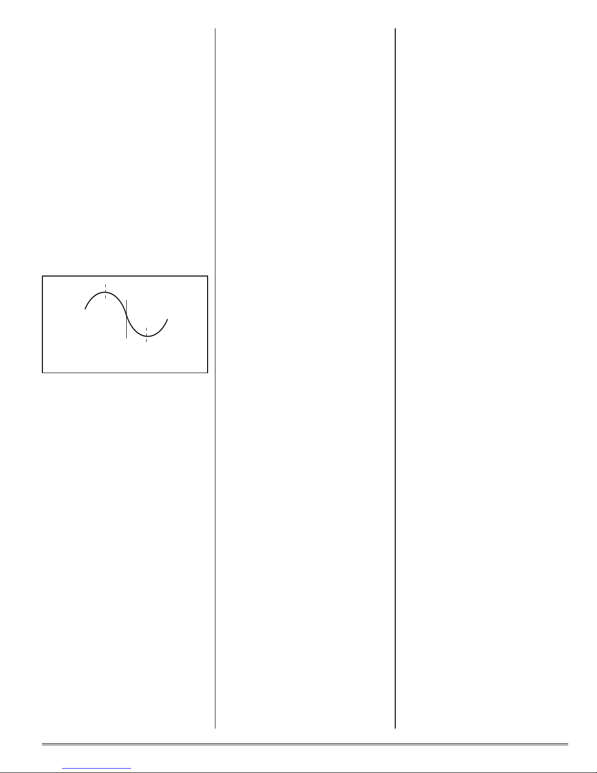
0 Be careful not to turn the slug
tight against either the top or bottom
because the winding of the transformer
can be broken. The tuning response is
an S-curve; so if you turn the slug several turns, you may think you are going
in the proper direction even though you
are tuning further away from center
frequency.
+3.3Vdc
Figure 1. Discriminator tuning
h. Connect signal generator to J1
using a coax cable with RCA plug.
Adjust signal generator to exact channel frequency, and turn output level
up fairly high (about 1000µV). Adjust
frequency trimmer in TCXO to net the
crystal to channel frequency, indicated by +3.3Vdc at test point TP-6.
Note: There are two methods of
adjusting the mixer and front end.
One is to use an fet voltmeter with test
point TP-5, which is the top lead of
R26. The voltage at this point is proportional to the amount of noise detected in the squelch circuit; so it
gives an indication of the quieting of
the receiver. With SQUELCH control
fully ccw, the dc voltage at TP-5 varies
from -0.5 Vdc with no signal (full
noise) to +0.8 Vdc with full quieting
signal.
The other method is to use a regular professional SINAD meter and a
tone modulated signal.
In either case, a weak to moderate
signal is required to observe any
change in noise. If the signal is too
strong, there will be no change in the
reading as tuning progresses; so keep
the signal generator turned down as
receiver sensitivity increases during
tuning.
If you use TP-5 with a voltmeter,
the signal can be modulated or unmodulated. If you use a SINAD meter,
the standard method is a 1000 Hz
tone with 3 kHz deviation.
i. Connect fet dc voltmeter to
TP5. Set signal generator for relatively
weak signal, one which shows some
change in the dc voltage indication at
TP5. Alternately peak RF amplifier
and mixer coils L4-L8 until no further
improvement can be made.
When properly tuned, sensitivity
should be about 0.15 to 0.2µV for 12
dB SINAD.
0 Mixer output transformer T1
normally should not be adjusted. It is
usually set exactly where it should be
right from the factory. The purpose of
the adjustment is to provide proper
loading for the crystal filter, and IF
misadjusted, ripple in the filter response will result in a little distortion
of the detected audio. If it becomes
necessary to adjust T1, tune the signal generator accurately on frequency
with about 4.5kHz fm deviation using
a 1000 Hz tone. In order of preference, use either a SINAD meter, an
oscilloscope, or just your ears, and
fine tune T1 for minimum distortion of
the detected audio.
THEORY OF OPERATION.
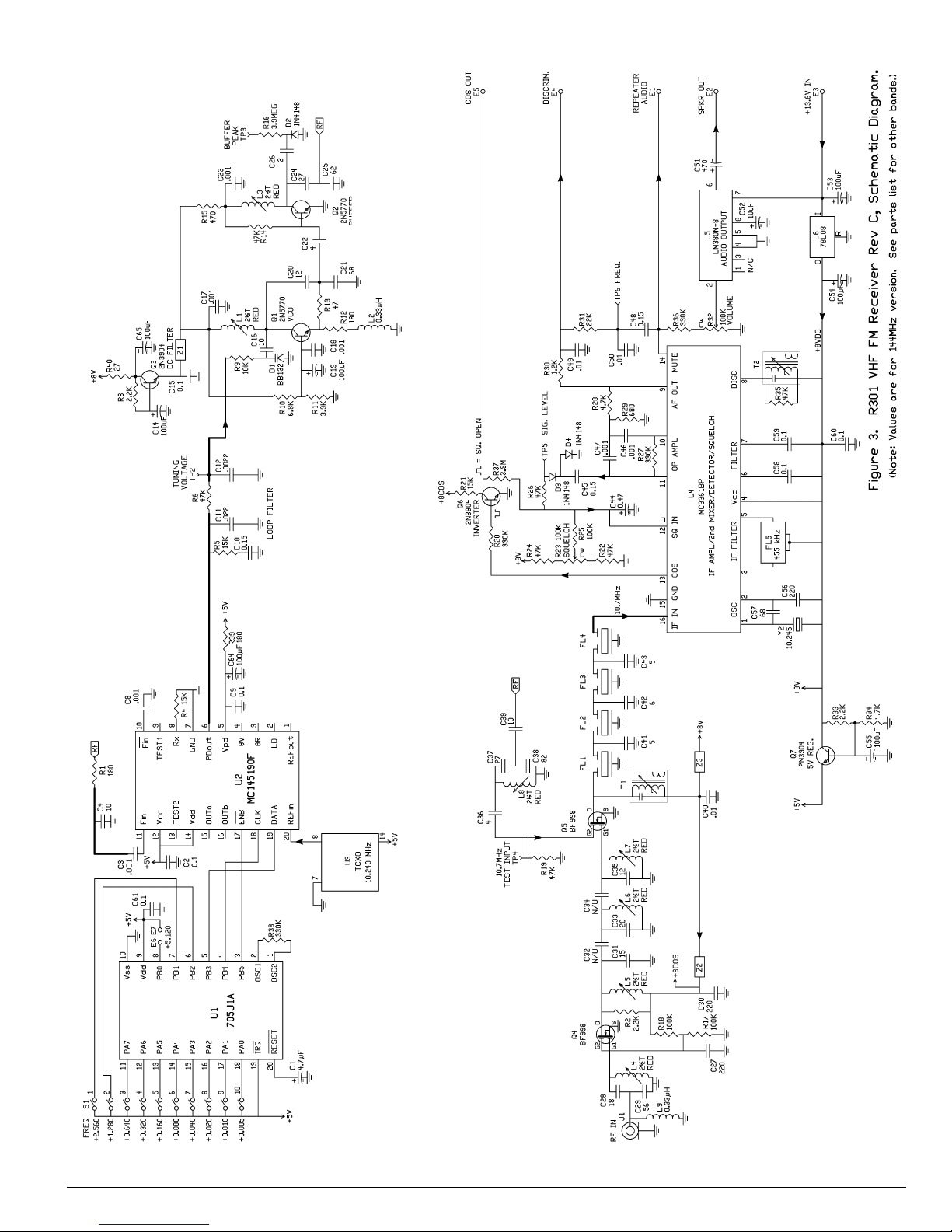
The R301 is a frequency synthesized vhf fm Receiver. Refer to the
schematic diagram for the following
discussion.
Low noise dual-gate mos fet’s are
used for the RF amplifier and mixer
stages. The output of mixer Q5
passes through an 8-pole crystal filter
to get exceptional adjacent channel
selectivity.
U4 provides IF amplification, a 2
mixer to convert to 455 kHz, a discriminator, noise amplifier, and
squelch. Ceramic filter FL5 provides
additional selectivity at 455 kHz. The
noise amplifier is an op amp active filter peaked at 10 kHz. It detects noise
at frequencies normally far above the
voice band. Its output at pin 11 is
rectified and combined with a dc voltage from the SQUELCH control to
turn a squelch transistor on and off
inside the ic, which grounds the audio
path when only noise is present. Inverter Q6 provides a dc output for use
as a COS signal to repeater controllers.
The injection frequency for the first
mixer is generated by vco (voltage controlled oscillator) Q1. The injection
frequency is 10.700 MHz below the
nd
receive channel frequency. The output of the vco is buffered by Q2 to
minimize effects of loading and voltage
variations of following stages from
modulating the carrier frequency. The
buffer output is applied through a
double tuned circuit to gate 2 of mixer
Q5.
The frequency of the vco stage is
controlled by phase locked loop synthesizer U2. A sample of the vco output is applied through the buffer stage
and R1/C3 to a prescaler in U2. The
prescaler and other dividers in the
synthesizer divide the sample down to
5kHz.
A reference frequency of 10.240
MHz is generated by a TCXO (temperature compensated crystal oscillator). The reference is divided down to
5 kHz.
The two 5kHz signals are compared to determine what error exists
between them. The result is a slowly
varying dc tuning voltage used to
phase lock the vco precisely onto the
desired channel frequency.
The tuning voltage is applied to
carrier tune varactor diode D1, which
varies its capacitance to tune the tank
circuit formed by L1/C20/C21. C16
limits the tuning range of D1. The
tuning voltage is applied to D1
through a third order low pass loop
filter, which removes the 5kHz reference frequency from the tuning voltage to avoid whine.
In order for the synthesizer to lock,
the vco must be tuned to allow it to
generate the proper frequency within
the range of voltages the phase detector in the synthesizer can generate,
roughly 1Vdc to 8Vdc.
Serial data to indicate the desired
channel frequency and other operational characteristics of the synthesizer are applied to synthesizer U2 by
microcontroller U1. Everything the
synthesizer needs to know about the
band, division schemes, reference frequency, and oscillator options is generated by the controller. Information
about the base frequency of the band
the Receiver is to operate on and the
channel within that band is calculated
in the controller based on information
programmed in the eprom on the controller and on channel settings done
on dip switch S1 and jumper E6-E7.
Whenever the microcontroller boots at
power up, the microcontroller sends
several bytes of serial data to the synthesizer, using the data, clock, and
/enable lines running between the two
ic’s.
©1998 Hamtronics, Inc.; Hilton NY; USA. All rights reserved. Hamtronics is a registered trademark. Revised: 12/11/02 - Page 4 -
Page 5

+13.6Vdc power for the Receiver is
applied at E1. Audio output amplifier
U5 is powered directly by the
+13.6Vdc. All the other stages are
powered through voltage regulators
for stability and to eliminate noise.
U6 is an 8Vdc regulator to power IF
amplifier U4, RF amplifier Q4, mixer
Q5, and the vco, buffer, and phase detector in the synthesizer. Additional
filtering for the vco and buffer stages
is provided by capacitance amplifier
Q3, which uses the characteristics of
an emitter follower to provide a very
stiff supply, eliminating any possible
noise on the power supply line. Q7
provides a stiff +5Vdc supply for the
frequency synthesizer and microcontroller, which are both low current
CMOS devices.
TROUBLESHOOTING.
General.
The usual troubleshooting techniques of checking dc voltages and
signal tracing with an RF voltmeter
probe and oscilloscope will work well
in troubleshooting the R301. DC voltage charts and a list of typical audio
levels are given to act as a guide to
troubleshooting. Although voltages
may vary widely from set to set and
under various operating and measurement conditions, the indications may
be helpful when used in a logical
troubleshooting procedure.
The most common troubles in all
kits are interchanged components,
cold solder joints, and solder
splashes. Another common trouble is
blown transistors and ic's due to reverse polarity or power line transients.
Remember if you encounter problems
during initial testing that it is easy to
install parts in the wrong place. Don't
take anything for granted. Double
check everything in the event of trouble.
Current Drain.
Power line current drain normally
is about 55 mA with volume turned
down or squelched and up to 200 mA
with full audio output.
If the current drain is approximately 100 mA with no audio output,
check to see if voltage regulator U6 is
hot. If so, and the voltage on the 8V
line is low, there is a short circuit on
the +8Vdc line somewhere and U6 is
limiting the short circuit current to
100mA to protect the receiver from
damage. If you clear the short circuit,
the voltage should rise again. U6
should not be damaged by short cir-
cuits on its output line; however, it
may be damaged by reverse voltage or
high transient voltages.
Audio Output Stage.
Note that audio output ic U5 is designed to be heatsunk to the pc board
through the many ground pins on the
ic. When running moderately low audio levels as most applications require, it is no problem to use an ic
socket; so we have provided one for
your convenience. If you will be running high audio levels, check to see if
the ic is getting hot. If so, you should
remove the ic socket, and solder the
LM-380N-8 ic directly to the board for
better heatsinking.
If audio is present at the volume
control but not at the speaker, the
audio ic may have been damaged by
reverse polarity or a transient on the
B+ line. This is fairly common with
lightning damage.
If no audio is present on the volume control, the squelch circuit may
not be operating properly. Check the
dc voltages, and look for noise in the
10 kHz region, which should be present at the top lead of R27 (U1-pin 11)
with no input signal. (Between pins
10 and 11 of U1 is an op-amp active
filter tuned to 10 kHz.)
RF Signal Tracing.
If the receiver is completely dead,
try a 10.700 MHz signal applied to
TP-4 (the top lead of R19), using coax
clip lead. Connect coax shield to pcb
ground. Set level just high enough for
full quieting. At 1 µV, you should notice some quieting, but you need
something near full quieting for the
test.
You can also connect the 10.700
MHz clip lead through a blocking capacitor to various sections of the crystal filter to see if there is a large loss of
signal across one of the filter sections.
Also, check the 10.245 MHz oscillator
with a scope or by listening with an hf
receiver or service monitor.
A signal generator on the channel
frequency can be injected at various
points in the front end. If the mixer is
more sensitive than the RF amplifier,
the RF stage is suspect. Check the dc
voltages looking for a damaged fet,
which can occur due to transients or
reverse polarity on the dc power line.
Also, it is possible to have the input
gate (gate 1) of the RF amplifier fet
damaged by high static charges or
high levels of RF on the antenna line,
with no apparent change in dc volt-
ages, since the input gate is normally
at dc ground.
Synthesizer Circuits.
Following is a checklist of things to
look for if the synthesizer is suspected
of not performing properly.
a. Check the output frequency of
the vco buffer with a frequency counter.
c. Check tuning voltage at TP2.
It should be about +4.0Vdc. Actual
range over which the unit will operate
is about +1Vdc to just under +8Vdc.
However, for optimum results, the vco
should be tuned to allow operation at
about +4.0Vdc center voltage.
d. Check the operating voltage
and bias on the vco and buffer.
e. Check the 10.240 MHz oscillator or TCXO at pin 1 of the synthesizer ic (actually best to check at top
lead of R3 or the pad which it would
be connected to; avoid trying to probe
surface mount ic leads which are
close together). A scope should show
strong signal (several volts p-p) at
10.240 MHz.
f. Check the oscillator at pin 1 of
microcontroller ic U1 with a scope.
There should be a strong ac signal
(several volts p-p) at the oscillator frequency.
g. The data, clock, and /enable
lines between the microcontroller and
synthesizer ic’s should show very brief
and very fast activity, sending data to
the synthesizer ic shortly after the
power is first applied or a dip switch
setting is changed. Because this happens very fast, it can be difficult to see
on a scope. Use 100µSec/div,
5Vdc/div, and normal trigger.
h. Check the microcontroller to
see that its /reset line is held low
momentarily when the power is first
applied. C1 works in conjunction
with an internal resistor and diode in
the ic to make C1 charge relatively
slowly when the power is applied. It
should take about a second to charge
up.
i. Check the switch and E6-E7
jumper settings to be sure you have
the correct frequency information going to the microcontroller.
j. If you have a scope or spectrum analyzer, you can check the
output pin of the divide by 64 prescaler at pin 13 of U2. There should be a
strong signal (several volts p-p) at
about 2.25 MHz. If this signal is absent, there may not be sufficient level
of sample signal from the buffer at U2
pin 11. Be careful not to short adja-
©1998 Hamtronics, Inc.; Hilton NY; USA. All rights reserved. Hamtronics is a registered trademark. Revised: 12/11/02 - Page 5 -
Page 6
cent pins of the ic.
Microphonics, Hum, and Noise.
The vco and loop filter are very
sensitive to hum and noise pickup
from magnetic and electrical sources.
Some designs use a shielded compartment for vco’s. We assume the
whole board will be installed in a
shielded enclosure; so we elected to
keep the size small by not using a
separate shield on the vco. However,
this means that you must use care to
keep wiring away from the vco circuit
at the right side of the board. Having
the board in a metal enclosure will
shield these sensitive circuits from florescent lights and other strong
sources of noise.
Because the frequency of a synthesizer basically results from a free running L-C oscillator, the tank circuit,
especially L1, is very sensitive to microphonics from mechanical noise
coupled to the coil. You should minimize any sources of vibration which
might be coupled to the Receiver,
such as motors. In addition, it helps
greatly to prevent the molded coil from
vibrating with respect to the shield
can. Both the coil and can are soldered to the board at the bottom, but
the top of the coil can move relative to
the can and therefore cause slight
changes in inductance which show up
as frequency modulation. Securing
the top of the plastic coil form to the
shield can with some type of cement
or nail polish greatly reduces the microphonic effects. This practice is
recommended in any installation
where vibration is a problem.
Excessive noise on the dc power
supply which operates the Receiver
can cause noise to modulate the synthesizer output. Various regulators
and filters in the Receiver are designed to minimize sensitivity to wiring noise. However, in extreme cases,
such as in mobile installations with
alternator whine, you may need to
add extra filtering in the power line to
prevent the noise from reaching the
Receiver.
Other usual practices for mobile
installations are recommended, such
as connecting the + power and ground
return lines directly to the battery instead of using cigarette lighter sockets
or dash board wiring.
To varying degrees, whine from the
5kHz reference frequency may be
heard on the signal under various circumstances. If the tuning voltage required to tune the vco on frequency is
very high or low, near one extreme,
the whine may be heard. This can
also happen even when the tuning
voltage is properly near the 4.0Vdc
center if there is dc loading on the
loop filter. Any current loading, no
matter how small, on the loop filter
causes the phase detector to pump
harder to maintain the tuning voltage.
The result is whine on the signal.
Such loading can be caused by connecting a voltmeter to TP2 for testing,
and it can also be caused by moisture
on the loop filter components.
Phase noise is a type of white noise
which phase locked loop synthesizers
produce. Many efforts are made during the design of the equipment to reduce it as much as possible. The
phase noise in this unit should be almost as good as a crystal oscillator
radio. If you notice excessive white
noise even though the signal is strong,
it may be caused by a noisy vco transistor, Q1. Try swapping with the
buffer transistor, Q2, which is the
same type and see if that helps.
When using a replacement transistor
for repairs, be sure to use one of good
quality.
If you suspect noise is being introduced in the synthesizer, as opposed
to the signal path from the antenna to
the detector, you can listen to the injection signal at 10.700 MHz below
the channel frequency on a receiver or
service monitor and hear what just
the injection signal sounds like. Put a
pickup lead on top of the Receiver
board so you have a strong sample to
hear so you are sure the noise is not
due to weak signal pickup at the test
receiver.
Typical Dc Voltages.
Tables 4-6 give dc levels measured
with a sensitive dc voltmeter on a
sample unit with 13.6 Vdc B+ applied.
All voltages may vary considerably
without necessarily indicating trouble.
The charts should be used with a logical troubleshooting plan. All voltages
are positive with respect to ground
except as indicated.
Use caution when measuring voltages on the surface mount ic. The
pins are close together, and it is easy
to short pins together and damage the
ic. We recommend trying to connect
meter to a nearby component connected to the pin under question.
Also, some pins are not used in this
design, and you can generally not be
concerned with making measurements on them.
Typical Audio Levels.
Table 7 gives rough measurements
of audio levels.. Measurements were
taken using an oscilloscope, with no
input signal, just white noise so conditions can be reproduced easily.
REPAIRS.
If you need to unsolder and replace
any components, be careful not to
damage the plated through holes on
the pc board. Do not drill out any
holes. If you need to remove solder,
use a solder sucker or solder wick. A
toothpick or dental probe can be used
with care to open up a hole.
If you need to replace surface
mount ic U2, first be very sure it is
damaged. Then, carefully cut each
lead off the case with fine nose cutters. Once the case is removed, individual leads can be unsoldered and
the board can be cleaned up. Carefully position the new ic, and tack solder the two opposite corner leads
before any other leads are soldered.
This allows you to melt the solder and
reposition the ic if necessary. Once
you are sure, the remaining leads can
be soldered. If you get a solder short
between leads, use a solder sucker or
solder wick to remove the excess solder.
Table 4. Typical Test Point Voltages
TP2 Tuning V. Normally set at 4.0V
TP3 Buffer approx. 0.5V (0.6V on
216-226 MHz band)
TP4 Test Input (No reading)
TP5 Sig. Level With SQUELCH control
fully ccw, varies from -0.5
Vdc with no to +0.75 Vdc
full quieting.
TP6 Freq. Varies with frequency of
input signal. Voltage at
this point normally is ad-
justed for +3.3Vdc with a
signal exactly on fre-
quency. Can vary a little
without being a problem.
Table 5. Typical Xstr DC Voltages
Xstr Stage E(S) B(G1) C(D) G2
Q1 vco 1.5 2.2 7.2 -
Q2 buffer 0 0.75 4.5 Q3 dc filter 7.2 7.8 8 Q4 RF ampl 0 0 8 4
Q5 Mixer 0 0 8 0
Q6 sq. open 0 0 8 sq. closed 0 0.66 0.1 Q7 5V regul. 5 5.7 8 -
©1998 Hamtronics, Inc.; Hilton NY; USA. All rights reserved. Hamtronics is a registered trademark. Revised: 12/11/02 - Page 6 -
Page 7
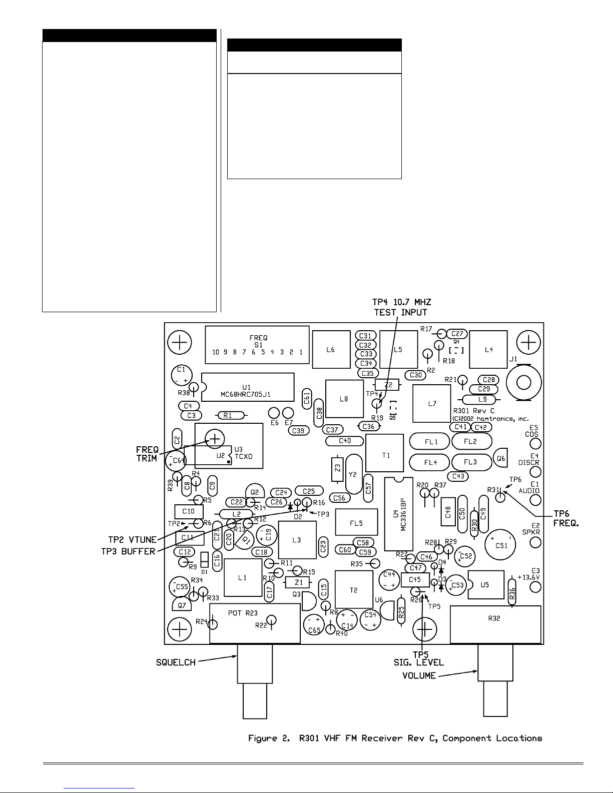
Table 6. Typical IC DC Voltages
U1-1 4 U1-2 4
U2-1 2.2 ‡ U2-10 2.5
U2-2 5V locked U2-11 2.5
(2.5V unlocked) U2-12 5
U2-3 8 * U2-13 3 *
U2-4 8 * U2-14 5
U2-5 8 U2-15 *
U2-6 0-8 (2.5V tuned) U2-16 *
U2-7 0 U2-17 5
U2-8 4.8 U2-18 0
U2-9 5 * U2-19 0
* = pin not used U2-20 2 ‡
‡ = xtal osc option
U4-1: 8 U4-10: 0.75
U4-2: 7.5 U4-11: 1.4
U4-3: 7.6 U4-12: 0.55 (with
U4-4: 8 sq. just closed)
U4-5: 7.6 U4-13:
U4-6: 7.6 0V (sq open),
U4-7: 7.6 7.6V (sq closed)
U4-8: 8 U4-14: 0
U4-9: 3.3 (Varies U4-15: 0
w/freq) U4-16: 1.8
U5-1: 0 U5-5: 0
U5-2: 0 U5-6: 6
U5-3: 0 U5-7: 13.6
U5-4: 0 U5-8: 7
Table 7. Typical Audio Voltages
Audio Test Point Normal Level
U4-9 (Discriminator) 3V p-p audio
E4 (Disc Output) 2V p-p audio
TP-6 1V p-p audio
E1 (Repeater Output) 1V p-p audio
U4-11, top of R27 2.5V p-p noise
(noise ampl output)
Top of Vol Cont R32 300mV p-p audio
U5-2 (af ampl input) 0 to 100mV p-p
(depends on vol
ume control)
U5-6 or E2 0 to 8V p-p audio
(speaker ampl output)
©1998 Hamtronics, Inc.; Hilton NY; USA. All rights reserved. Hamtronics is a registered trademark. Revised: 12/11/02 - Page 7 -
Page 8
PARTS LIST FOR R301
RECEIVER.
☞ Note: Values which vary with freq. band
are shown in a table at the end of the parts list.
Capacitors are disc type unless noted otherwise.
➊ Resistors used as test point or external
connection point. These must be installed on
the board oriented properly and with the top
loop an extra 1/6” high to allow for connections
to the loop later. (See detail in component location diagram.)
➋ Microcontroller must be factory programmed for proper band segment and for
TCXO or crystal osc option.
➌ This part must be installed with a small
space (about the thickness of an index card)
under the part to prevent the bottom of the part
from shorting to the ground plane.
0 Caution: IC’s are static sensitive. Use
appropriate handling precautions to avoid damage.
Ref Desig Value (marking)
C1 not used
C2 0.1µf monolithic (104)
C3 .001 uf (102, 1nM, or 1nK)
C5-C7 not assigned
C8 .001 uf (102, 1nM, or 1nK)
C9 0.1µf monolithic (104)
C10 0.15µf mylar (red)
C11 .022µf mylar (223)
C12 .0022µf (2.2nK or 222)
C13 not assigned
C14 10µf electrolytic
C15 0.1µf monolithic (104)
C19 10µf electrolytic
C22 4pf
C26 2pf
C32 not used
C34 not used
C36 4pf
C40 .01µf (103)
C41 5pf
C42 6pf
C43 5pf
C44 0.47µf electrolytic
C45 0.15µf mylar (red)
C46-C47 .001 uf (102, 1nM, or 1nK)
C48 0.15µf mylar (red)
C49-C50 .01µf (103)
C51 470µf electrolytic
C52 10µf electrolytic
C53 1µf electrolytic
C54 100µf electrolytic
C55 not used
C56 220pf (221)
C57 68pf
C58-C61 0.1µf monolithic (104)
C62-C63 not used
C64 10 µf electrolytic
C65 100 µf electrolytic
D1 BB132 varactor diode
(surface mt under board)
D2-D4 1N4148 switching diode
FL1-FL4 ➌ 10.7MHz crystal filter
(matched set of 4)
FL5 455kHz ceramic filter
J1 RCA Jack
L2 0.33µH RF choke
(red-sil-orn-orn)
L3-L8 2½ t. ,slug tuned (red)
L9 0.33µH RF choke
(red-sil-orn-orn)
Q1-Q2 2N5770
Q3 2N3904
Q4-Q5 BF998 MOS FET (surface
mount under board)
Q6 2N5770
Q7 2N3904
R1 180Ω
R2 not used
R3 not assigned
R4 47K
R5 15K
R6 ➊ 47K
R7 not assigned
R8 2.2K
R9 10K
R10 6.8K
R11 3.9K
R12 180Ω
R13 47Ω
R14 47K
R15 470Ω
R16 ➊ 3.9meg
R17-R18 100K
R19 ➊ 47K
R20 330K
R21 15K
R22 47K
R23 100K panel mount pot.
R24 47K
R25 100K
R26 ➊ 47K
R27 330K
R28 4.7K
R29 680Ω
R30 1.2K
R31 ➊ 22K
R32 100K panel mount pot.
R33 2.2K
R34 4.7K
R35 47K
R36 330K
R37 3.9meg
R38 2meg
R39 180Ω
R40 27Ω
S1 10 pos. DIP switch
T1 10.7MHz IF xfmr
(7A-691F)
T2 455kHz IF transformer
(T1003)
U1 0➋ MC68HC705J1A µP
U2 0 MC145190F
(surface mt under board)
U3 0 10.240 MHz TCXO
U4 MC3361BP IF ampl
U5 LM380N-8 af output
U6 78L08 regulator
Y2 ➌ 10.245 MHz crystal
Z1-Z3 Ferrite bead, prestrung
VALUES WHICH VARY WITH
FREQUENCY BAND:
R301-2 is 144.000 - 154.235 MHz
R301-3 is 154.200 - 164.435 MHz
R301-4 is 164.400 - 174.635 MHz
R301-5 is 216.000 - 226.235 MHz
R301-6 is 220.000 - 230.235 MHz
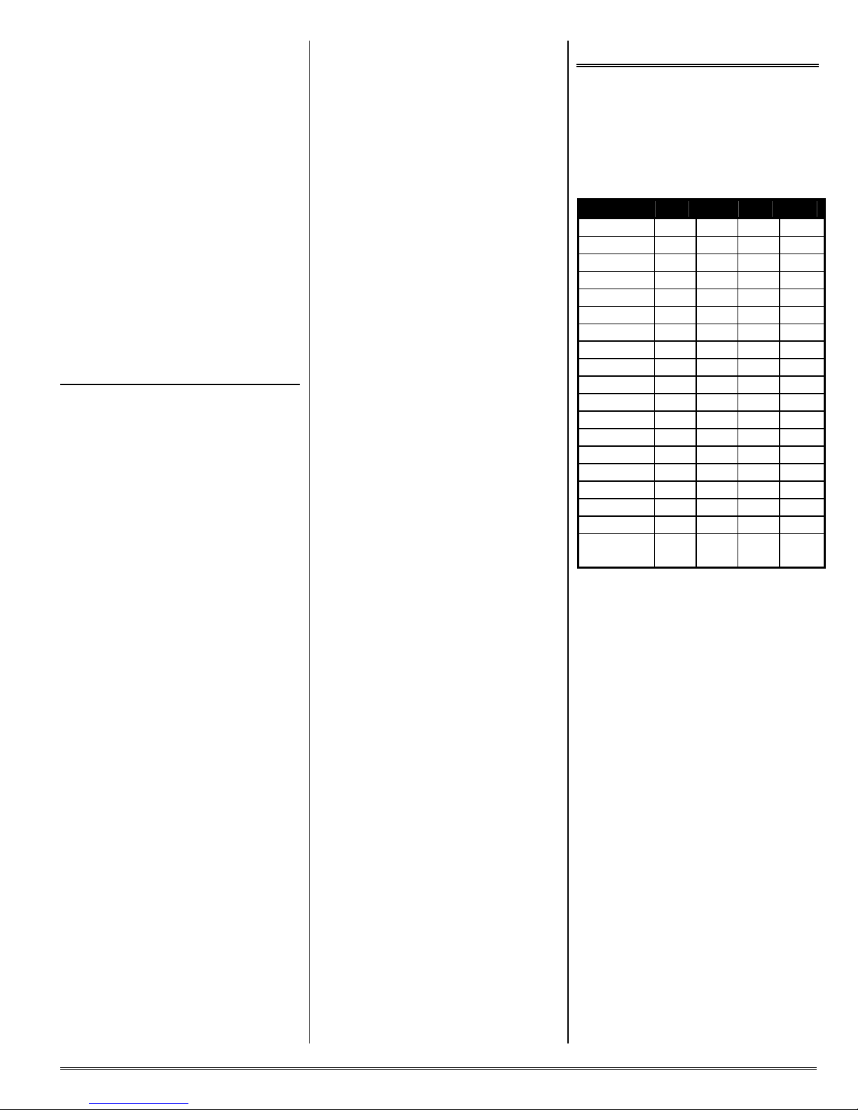
Ref Desig -2 -3 -4 -5/-6
C4 10 10 10 n/u
C16 10 10 10 8
C17, C18 .001 .001 .001 220
C20 12 10 8 11
C21 68 62 47 47
C23 .001 .001 .001 100
C24 27 22 18 8
C25 62 47 47 27
C27 220 220 220 100
C28 20 18 15 5
C29 56 47 43 15
C30 220 220 220 100
C31 18 15 12 6
C33 20 18 15 7
C35 15 15 12 4
C37 27 22 20 9
C38 82 62 56 27
C39 10 8 8 3
L1 2½T
(red)
2½T
(red)
2½T
(red)
1½T
(brn)
©1998 Hamtronics, Inc.; Hilton NY; USA. All rights reserved. Hamtronics is a registered trademark. Revised: 12/11/02 - Page 2 -
Page 9
©1998 Hamtronics, Inc.; Hilton NY; USA. All rights reserved. Hamtronics is a registered trademark. Revised: 12/11/02 - Page 3 -
 Loading...