

Page 1

©
2009
Hamtronics, Inc.; Hilton NY; USA. All rights reserved. Hamtronics is a registered trademark. Revised:
7/28/11
-
Page
1-
HAMTRONICS® R100 VHF FM RECEIVER:
ASSEMBLY, INSTALLATION, OPERATION, & MAINTENANCE
Note about page numbers.
In order to accommodate various bands,
this manual has extra pages you may not receive for your version. The two meter version
will have pages numbered 1 through 7. Other
bands may have a higher number page substituted for the two meter parts list page, so
pages may not all be consecutive.
FUNCTIONAL DESCRIPTION.
The R100 is a commercial-grade singlechannel vhf fm receiver available in models for
various bands, both in kit form and factory
wired and tested.
The R100 features a front end with lownoise dual gate fet's and triple-tuned circuits
for excellent sensitivity and rejection of outof-band interference. It has an 8-pole crystal
filter with steep skirts plus a ceramic filter for
close channel spacing or repeater operation.
The i-f selectivity, for instance, is down over
100dB at ±12 kHz away from the carrier,
which is 40-50 dB better than most transceivers.
A new positive-acting, wide-range squelch
circuit locks onto fading signals. The R100 has
output terminals for low-level squelched audio and discriminator audio as well as speaker
audio and a COS logic signal from the squelch
circuit.
ASSEMBLY.
General Information.
Note that vhf equipment requires pre-
cise construction using short, direct leads.
Seat parts as close to the board as possible
without over-stressing the leads.
Be sure to follow instructions as given and
don't arbitrarily do things differently.
When installing resistors and diodes that
are mounted vertically, be sure to orient the
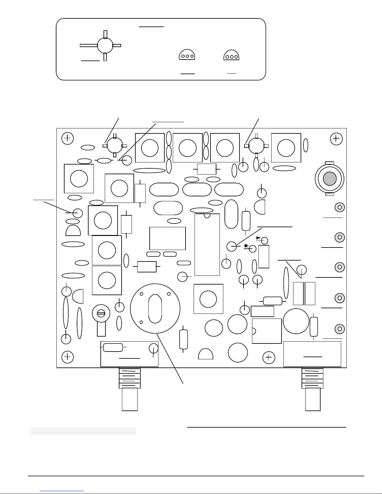
body as shown by large circles in parts location diagram.
Static handling precautions are re-
quired for the fet's. The small geometry and
high impedances make FET's heat and static
sensitive; so be careful. It is good to discharge
your hand to a grounded metal object just before picking up a transistor, and the use of a
grounded soldering iron is mandatory.
Assembly Procedure.
a. Set board on bench or in holding jig
oriented as shown.
b. Install phono jack J1, orienting the
center lug toward the inside of the board
where the large pad is located under the
board. Bend the center tab over against the
foil, and solder all tabs under board.
c. Install FET's Q1 & Q2 from top of
board. ORIENT THEM AS SHOWN with the
long drain lead positioned as indicated. Note
that the LETTERING MUST BE UP, not against
the board. Gently bend the leads of the fet's
at right angles, and insert into the holes in the
board. Seat the transistors as close to board
as possible without straining leads. Solder
leads under board.
d. The crystal filters must be installed
with uncoded ends to the outside world and
the terminals which are connected to each
other all with matching color dots. The idea is
to connect these tandem filters in the circuit
in the same sequence as they were matched
at the factory. Start with either filter having
only one color dot. Install in position FL1 with
color dot to the right as shown.
e. Install the filter with the matching
color dot in position FL2 so that matching
color dots on FL1 and FL2 are adjacent to each
other.
f. Likewise, install FL3 with upper color
dot to match right-hand dot on FL2. Then, install FL4 with only one remaining color dot adjacent to matching color dot on FL3.
g. Install ferrite beads Z1-Z4, and solder
leads to board.
h. Install diodes CR1 and CR2, observing
polarity. Note that the banded ends of the diodes should be down.
i. Install transistors Q3-Q5 and voltage
regulator U3, observing proper orientation.
j. U1 and U2 have a dot over pin 1 or a
notch in that end for identification as shown
in diagram. Solder the ic’s in place, being
careful about polarity.
Also note that using a socket is not recommended for i-f amplifier U1 because of the
extra inductance the socket would add to the
high frequency circuits, and audio output ic U2
needs to be heatsunk to the ground plane on
the board. Therefore, ic sockets have not
been supplied.
k. Install electrolytic capacitors, observing polarity.
l. Install slug tuned coils and transformers as shown, and install coil shields. The 2½
turn (red) coils come with shields already on
the coils; however, in some cases, the shield
must be removed and rotated 90° in order to
fit holes in pc board. The 6½ turn (blue) coils
have shields supplied separately.
Note: Wait to install L3 after all other
parts are installed. It is easier to install adjacent capacitors before L3 is mounted.
m. Make sure the coils and shields are
fully seated, and solder both shield lugs. (Do
not bend lugs over, but you can bend the coil
leads over a little to hold them in place while
soldering.)
o. Install socket pins at Y1. Cut socket
pins from carrier strip close to body. Rock
them while firmly pressing into board. They
will snap in place. Solder lightly under board
(to avoid solder filling crystal sockets).
p. Install all remaining components as
per location diagram and parts list. Leave the
top leads of R3, R7, R13, and R18 about 1/8"
high to act as test points. R4 and R5 each use
two 6.8K resistors tack soldered together at
the top to give 14K total resistance.
q. Install pots R10 and R20. They should
be held in position while soldering so shafts
are at right angles to board, thereby minimizing strain on leads when pots are later secured to front panel.
r. Install L3.
s. Check over all parts and solder connections. If you are missing any parts, check
to see if you have other parts left over. You
may have installed a wrong value somewhere;
so recheck all values looking for the missing
parts. Color codes and printed numbers are
difficult to read on many small parts, so special care is sometimes needed to avoid mixups. Note that on certain models, some parts
may be marked "not used" in the parts list.
CRYSTALS.
The channel crystal plugs into sockets on
the board. We can supply crystals for any frequency desired. We recommend that any new
crystals be ordered directly from us to be sure
that they will perform properly over the -30 to
+60°C range for which the unit was designed.
If you do order elsewhere, be sure to supply
the following specs.
The receiver uses 32 pF parallel resonant
crystals in HC-25/u holders. Crystals operate
in the fundamental mode. The crystal frequency is as noted in the table below. Frequency tolerance is .001%. If you use an OV-1
crystal oven, specify a crystal with a 60°C
breakpoint.
Note: If your crystal has a metal base,
avoid pushing the crystal down tight against
the sockets. After installing a crystal, simply
lift it slightly to be sure the base doesn't touch
Specifications of Interest
Frequency Range: R100-50, 46-54 MHz
R100-72, 72-76MHz
R100-144, 140-175 MHz
R100-220, 216-225 MHz
Sensitivity (12dB SINAD): 0.15uV
Squelch Sensitivity: 0.1µV
Selectivity: ±12 kHz at -100dB
Modulation Acceptance: ±7.5 kHz
IF Filters: 8 pole 10.7 MHz crystal filter plus
455 kHz ceramic filter.
Audio Output: 2 Watts (8 ohms).
Operating Power: +13.6Vdc at 45-120 mA,
depending on audio level.
Size: 4 in. W x 3-7/16 in. D (plus pot. shafts)
Page 2
©
2009
Hamtronics, Inc.; Hilton NY; USA. All rights reserved. Hamtronics is a registered trademark. Revised:
7/28/11
-
Page
2-
the sockets. If you use a crystal oven, when
you install it, push it down over the crystal and
stop pushing when you feel the oven contact
the top of the crystal.
Crystal Frequency Formula
R100-50, 46-54 MHz ------------ (F-10.7)/3
R100-72, 72-76MHz ------------- (F-10.7)/4
R100-144, 140-175 MHz ------- (F-10.7)/9
R100-220, 216-225 MHz ------ (F-10.7)/12
INSTALLATION.
Power Connections.
The receiver operates on +13.6 Vdc at
about 120 mA peak with full audio. Current
drain with no audio is only about 45 mA. A
crystal oven adds about 450 mA peak current
drain when cold and only about 25 mA when
warm. A well regulated power supply should
be used.
Be sure that the power source does not
carry high voltage or reverse polarity transients on the line, since semiconductors in the
receiver can be damaged. The positive power
supply lead should be connected to the receiver at terminal E3, and the negative power
lead should be connected to the ground plane
of the board through the mounting hardware
or the shield of the coaxial cable. Be sure to
observe polarity!
Speaker.
An 8-ohm loudspeaker should be connected to E2 with ground return through the
mounting hardware. Use of lower impedance
speaker or shorting of speaker terminal can
result in ic damage. The receiver can also
drive higher impedances, like 1K to 10K input
impedances of COR boards, etc. There is no
need to load down the output to 8 ohms.
Note that the audio output ic is designed
to be heatsunk to the pc board through the
many ground pins on the ic. When running
moderately low audio levels as most applications require, it is no problem to use an ic
socket; so we have provided one for your convenience. If you will be running high audio
levels, check to see if the ic is getting hot. If
so, you should remove the ic socket, and solder the LM-380N-8 ic directly to the board for
better heatsinking.
Antenna Connections.
The antenna connection should be made
to the pc board with an RCA plug of the lowloss type made for rf. We sell good RCA plugs
with cable clamp. See A5 plug on website.
If you want to extend the antenna connection to a panel connector, we recommend
using a short length of RG-174/u coax with the
plug and keep the pigtails very short.
We do not recommend trying to use direct
coax soldered to board or another type of
connector. The method designed into the
board results in lowest loss practical. When
soldering the cable, keep the stripped ends as
short as possible.
We recommend you always use anten-
nas with a matching network which provides a
dc ground on the driven element. This reduces
chances of static buildup damaging the input
stage of the receiver as well as providing
safety for the building and other equipment.
OPTIONS.
Repeater Use.
E4 provides a COS (carrier operated
switch) output which may be connected to a
COR module to turn a transmitter on and off.
The output level is about 8V unsquelched and
0V squelched. There is a resistor in series with
the output to limit current. Therefore, the
voltage that appears at the COR board will depend on the load resistance at the input of
that board. For best results, be sure that the
input resistance of the COR board is at least
47K. If the input resistance is too low, no
damage to the receiver will occur; but the
squelch circuit hysteresis will be affected.
If your repeater controller uses discriminator audio, rather than the speaker output,
filtered discriminator audio is available at E5.
The level is about 2V p-p. Note that discrimi-
nator audio is not de-emphasized. If you need
audio which is squelched, take it from Repeater Audio terminal E1.
If your controller uses low level audio and
has a high input impedance (20K or higher),
squelched audio can be obtained from E1 independent of the VOLUME control.
Discriminator Meter.
If you wish to use a discriminator meter
and you are handy in designing with op-amps,
you can run a sample of the dc voltage at DIS-
CRIMINATOR output terminal E5 to one input
of an op-amp and tie the other input to a voltage divider pot set to provide a reference voltage of about +3.3Vdc.
S-Meter.
There is no s-meter function, as such,
available in i-f amplifier ic's made for professional receivers; however, a signal strength indication is available at test point TP-2. This
voltage is a function of the noise level detected in the squelch circuit. It also varies
with SQUELCH control setting. With the
SQUELCH set to where the squelch just closes,
the dc voltage at TP-2 is about -0.55V with no
signal and +0.75 with full quieting signal. You
can tap off this test point with a highimpedance circuit, such as an op-amp, to drive
a meter or a computerized repeater controller.
Subaudible Tone Decoder.
To use our TD-5 Subaudible Tone Decoder
or a similar module, connect its audio input to
DISCRIMINATOR terminal E5. If you want to
use it to mute the audio (instead of inhibiting
a repeater transmitter as is normally done),
connect the mute output of the TD-5 to E1 on
the receiver.
ALIGNMENT.
Equipment needed for alignment is an fet
voltmeter, an rf signal generator, a regulated
13.6Vdc power supply with a 0-200 mA meter
internally or externally connected in the supply line.
The slug tuned coils in the receiver should
be adjusted with the proper aluminum .062"
square tuning tool to avoid cracking the powdered iron slugs. The variable capacitor should
be adjusted with a plastic tool with a small
metal bit on the end. Tools are available for
adjusting the rf coils (model A28) and variable
capacitor (model A2).
The SQUELCH pot should be set fully counterclockwise. The VOLUME pot should be set
just a little clockwise.
a. Install channel crystal in socket.
b. Connect speaker and +13.6 Vdc. You
should hear white noise.
c. Connect dc voltmeter to TP-1 (top lead
of R7 on left side of board). Adjust first L7,
then L6 and L7 alternately for maximum response. (Approx. +1 to 2 Vdc typical.)
d. Connect stable signal generator to TP-4
(the top lead of R3), using coax clip lead.
Connect coax shield to pcb ground. Set generator to exactly 10.7000 MHz. Use a frequency counter or synthesized signal
generator. Set level just high enough for full
quieting. At 2 uV, you should notice some
quieting, but you need something near full
quieting for the test.
e. Connect dc voltmeter to TP-3 (top lead
of R18 on right side of board). Adjust discriminator transformer L10 for +3.3Vdc. Note that
the transformer is fairly close from the factory
and usually only requires less than ¼ turn in
either direction.
Be careful not to turn the slug tight
against either the top or bottom because the
winding of the transformer can be broken.
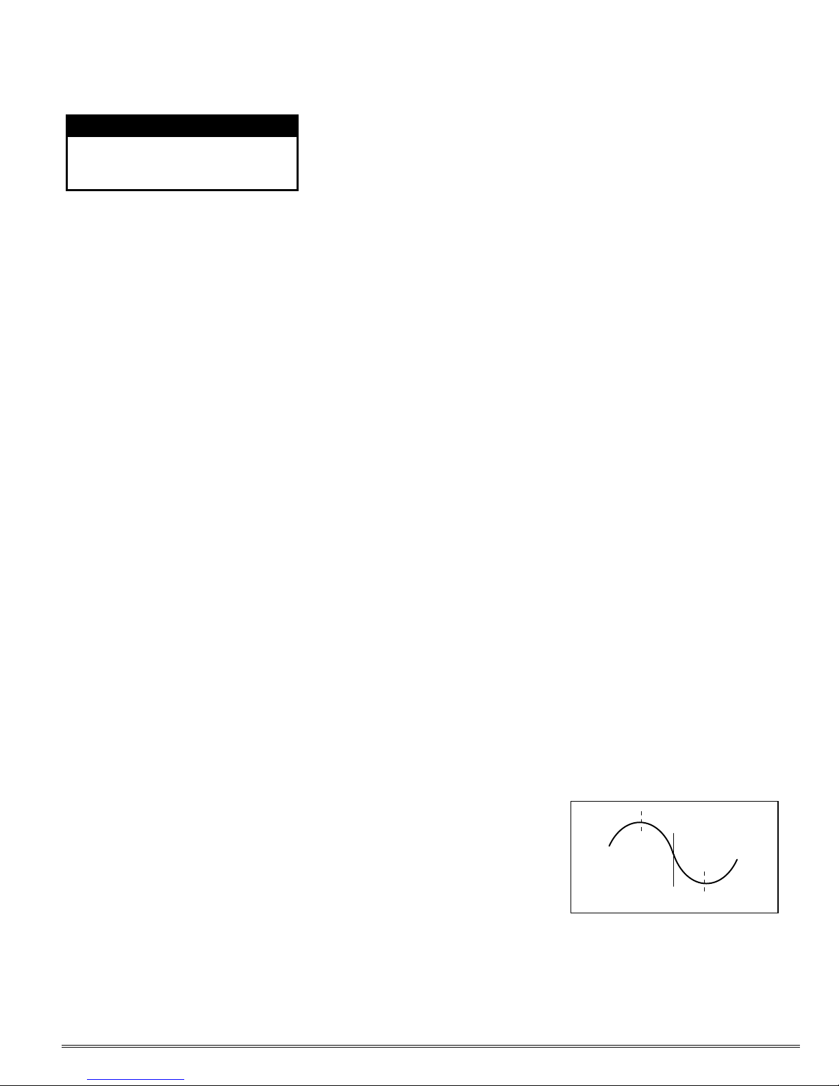
The tuning response is an S-curve; so if you
turn the slug several turns, you may think you
are going in the proper direction even though
you are tuning further away from center frequency.
+3.3Vdc
f. Connect signal generator to J1 using a
coax cable with RCA plug. Adjust signal generator to exact channel frequency, and turn
output level up fairly high (full quieting). Adjust frequency trimmer capacitor C15 to net
the crystal to channel frequency, indicated by
Page 3
©
2009
Hamtronics, Inc.; Hilton NY; USA. All rights reserved. Hamtronics is a registered trademark. Revised:
7/28/11
-
Page
3-
+3.3Vdc at test point TP-3.
➠
If you can't find the signal at all, tune
your signal generator up and down the band
slightly. Also check that oscillator is peaked as
per step c. If your crystal has the wrong load
correlation or is slightly out of tolerance, you
may be able to compensate by changing the
value of C16 so C15 can net the crystal on frequency. The piston capacitor tuning range is
restricted to provide best frequency stability;
so sometimes it may be necessary to change
the fixed capacitor. The proper adjustment
results in +3.3Vdc, the same as preset for the
exact 10.700 MHz i-f frequency earlier.
Maximum capacitance (lowest frequency)
occurs with the piston screwed in all the way,
and minimum capacitance (highest frequency)
is with the piston all the way up. Be careful
not to completely remove the piston. If the
piston screw becomes a little tight (squeaky),
you can apply a small amount of silicone oil to
the threads.
Note: There are two methods of adjusting
the mixer and front end. One is to use an fet
voltmeter with test point TP-2, which is the
top lead of R13. The voltage at this point is
proportional to the amount of noise detected
in the squelch circuit; so it gives an indication
of the quieting of the receiver. With SQUELCH
control fully ccw, the dc voltage at TP-2 varies
from -0.5 Vdc with no signal (full noise) to
+0.8 Vdc with full quieting signal.
The other method is to use a regular professional SINAD meter and a tone modulated
signal.
In either case, a weak to moderate signal
is required to observe any change in noise. If
the signal is too strong, there will be no
change in the reading as tuning progresses; so
keep the signal generator turned down as receiver sensitivity increases during tuning.
If you use TP-2 with a voltmeter, the signal
can be modulated or unmodulated. If you use
a SINAD meter, the standard method is a 1000
Hz tone with 3 kHz deviation.
g. Connect fet dc voltmeter to TP-2 (top
lead of R13). Set signal generator for relatively weak signal, one which shows some
change in the dc voltage indication at TP2. Alternately peak multiplier coils L8 and L9 until
no further improvement can be made.
h. Likewise, alternately adjust rf amplifier
coils L1-L4 until no further improvement can
be made.
When properly tuned, sensitivity should
be about 0.15 to 0.2 µV for 12 dB SINAD.
Mixer output transformer L5 normally
should not be adjusted. It is usually set exactly where it should be right from the factory. The purpose of the adjustment is to
provide proper loading for the crystal filter,
and if misadjusted, ripple in the filter response
will result in a little distortion of the detected
audio. If it becomes necessary to adjust L5,
tune the signal generator accurately on fre-
quency with about 3kHz fm deviation using a
1000 Hz tone. In order of preference, use either a SINAD meter, an oscilloscope, or just
your ears, and fine tune L5 for minimum distortion of the detected audio.
TROUBLESHOOTING.
The usual troubleshooting techniques of
checking dc voltages and signal tracing work
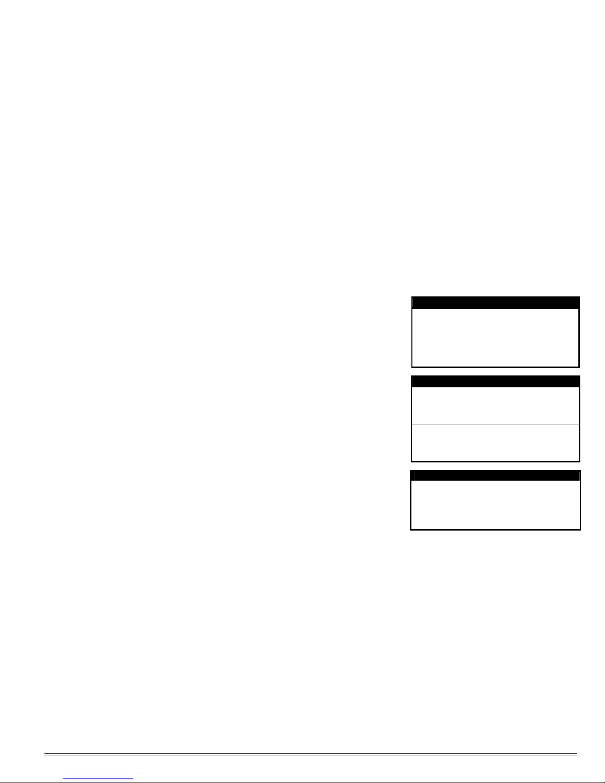
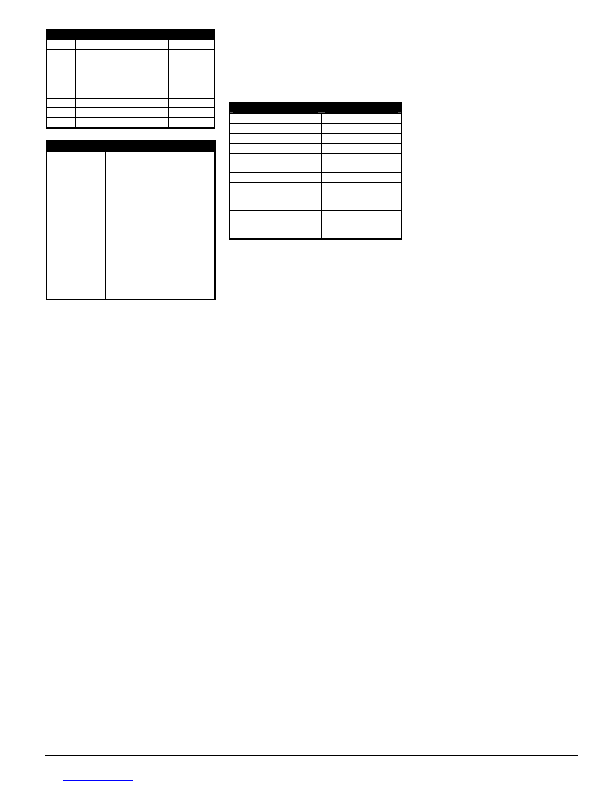
well in troubleshooting the receiver. DC voltage charts and a list of typical audio levels are
given to act as a guide to troubleshooting. Although voltages may vary widely from set to
set and under various operating and measurement conditions, the indications may be
helpful when used in a logical troubleshooting
procedure.
The most common troubles in all kits are
interchanged components, cold solder joints,
and solder splashes. Another common trouble is blown transistors and ic's due to reverse
polarity or power line transients. Remember
if you encounter problems during initial testing that it is easy to install parts in the wrong
place. Don't take anything for granted. Double check everything in the event of trouble.
Signal Tracing.
If the receiver is completely dead, try a
10.700 MHz signal applied to TP-4 (the top
lead of R3), using coax clip lead. Connect coax
shield to pcb ground. Set level just high
enough for full quieting. At 2 uV, you should
notice some quieting, but you need something
near full quieting for the test.
You can also connect the 10.700 MHz clip
lead through a blocking capacitor to various
sections of the crystal filter to see if there is a
large loss of signal across one of the filter sections. Also, check the 10.245 MHz oscillator
with a scope or by listening with an hf receiver
or service monitor.
A signal generator on the channel frequency can be injected at various points in the
front end. If the mixer is more sensitive than
the rf amplifier, the rf stage is suspect. Check
the dc voltages looking for a damaged fet,
which can occur due to transients or reverse
polarity on the dc power line. Also, it is possible to have the input gate (gate 1) of the rf
amplifier fet damaged by high static charges
or high levels of rf on the antenna line, with
no apparent change in dc voltages, since the
input gate is normally at dc ground.
If audio is present at the volume control
but not at the speaker, the audio ic may have
been damaged by reverse polarity or a transient on the B+ line. This is fairly common
with lightning damage.
If no audio is present on the volume control, the squelch circuit may not be operating
properly. Check the dc voltages, and look for
noise in the 10 kHz region, which should be
present at the top lead of R14 (U1-pin 11)
with no input signal. (Between pins 10 and 11
of U1 is an op-amp active filter tuned to 10
kHz.)
Current Drain.
Power line current drain normally is about
45mA with volume turned down or squelched
and up to 120 mA with full audio output.
If the current drain is approximately 100
mA with no audio output, check to see if voltage regulator U3 is hot. If so, and the voltage
on the 8V line is low, there is a short circuit on
the +8Vdc line somewhere and U3 is limiting
the short circuit current to 100mA to protect
the receiver from further damage. If you clear
the short circuit, the voltage should rise again.
U3 should not be damaged by short circuits on
its output line; however, it may be damaged
by reverse voltage or high transient voltages.
Test Point Indications.
The following measurements are typical of
those found at the three built-in test points
used for alignment. They can vary considerably without necessarily indicating a problem,
however; so use with other findings to analyze
problems, don't jump to conclusions.
Oscillator Test Point 1
Approx. +1 to 2 Vdc with osc running and
output tuned circuits aligned. Varies as
L6 and L7 are aligned. 0Vdc with oscillator not running or coils not properly
aligned. Not used on 50 MHz model.
Signal Strength Test Point 2
With SQUELCH control fully ccw, the dc
voltage at TP-2 varies from -0.5 Vdc with
no signal (full noise) to +0.8 Vdc with full
quieting signal.
With the SQUELCH control set to where
the squelch just closes, the dc voltage at
TP-2 varies from about -0.55V with no signal to +0.75 with full quieting signal
Discriminator Test Point 3
Varies with frequency of input signal. Voltage at this point normally is adjusted for
+3.3Vdc with a signal exactly on frequency.
Can vary a little without being a problem.
Typical Dc Voltages.
The following dc levels were measured
with an fet voltmeter on a sample unit with
+13.6 Vdc power applied. All voltages may
vary considerably without necessarily indicating trouble. The chart should be used with a
logical troubleshooting plan.
All voltages are positive with respect to
ground except as indicated. Voltages are
measured with no signal applied but with crystal(s) installed and oscillator(s) running properly and with squelch open unless otherwise
specified.
Page 4
©
2009
Hamtronics, Inc.; Hilton NY; USA. All rights reserved. Hamtronics is a registered trademark. Revised:
7/28/11
-
Page
4-
XSTR Cond. E(S) B(G1) C(D) G2
Q1 0 0 8 4
Q2 0 0 8 0
Q3 w/xtal 4.4 3.5 8 no xtal 3.2 3.9 8 Q4 drive 1 - 2 0 8 -
no drive 0 0 8 Q5 sq open 0 0 8
sq closed 0 0.66 0.1
IC Measurements
U1-1: 7.8V
U1-2: 7.4V
U1-3: 7.6V
U1-4: 8V
U1-5: 7.6
U1-6: 7.6V
U1-7: 7.6V
U1-8: 8V
U1-9: 3.3V
(On freq.;
Varies
w/freq)
U1-10:
0.75V
U1-11:
1.45V U112: 0.8V
(with
squelch just
closed)
U1-13:
0V (sq
open),
7.6V
(sq closed)
U1-14: 0V
U1-15: 0V
U1-16: 1.8V
U2-1: 0V
U2-2:
0.5V
U2-3: 0V
U2-4: 0V
U2-5: 0V
U2-6: 7V
U2-7:
13.6V
U2-8:
6.8V
Typical Audio Levels.
Following are rough measurements of audio circuits, using an oscilloscope. Measurements were taken with no input signal, just
white noise so conditions can be reproduced
easily.
Audio Test Point Normal Level
U1-9 (Discriminator) 3V p-p audio
E5 (Disc Output) 2V p-p audio
TP-3 100mV p-p audio
E1 (Repeater Output) 100mV p-p audio
U1-11, top of R14
(noise ampl output)
Top of Vol Cont R20 100mV p-p audio
U2-3 (af ampl input) 0 to 100mV p-p
U2-6 or E2
(speaker ampl output)
2V p-p noise
(depends on volume control)
0 to 3V p-p audio
Page 5
©
2009
Hamtronics, Inc.; Hilton NY; USA. All rights reserved. Hamtronics is a registered trademark. Revised:
7/28/11
-
Page
5-
SOURCE
Figure 1. R100 Receiver, Component Location Diagram
DRAIN
GAT E 1
Q1 & Q2
GAT E 2
LETTERING ON F.E.T. MUST BE
VISIBLE FROM TOP OF BOARD
TOP VIEWS
E B C
Q3-Q5
OUTPUT GND INPUT
U3
OSC TP-1
LONG DRAIN LEAD
C27
C26
L9
Q3
R7
C23
C21
C18
C24
C25
Q4
C22
C20
R5
C17
R6
C10
L8
C15
L7
L6
Q2
R9
R3
L5
C16
SQUELCH
Z3
C19
R4
R10
10.7 MHz TP-4
L4
C11
Z2
C43
R11
FL1
Y2
C40
FL5
Z4
Y1
C
7
C
8
C
9
C42
R12
C41
C12
R21
L3
C39
FL2
C
5
C
6
Z1
C14
1
U1
IF Ampl.
8
L10
U3
16
+
C28
_
9
LONG DRAIN LEAD
L2
C4
C13
FL3
FL4
R13
C31
R14
R22
+
C35
_
+
C36
_
Q1
R1 C3 R2 C2 J1
R23
Q5
R8
SIG . LEVEL TP-2
CR2
CR1
C29
C30
R16 R15
C37
8
U2
Audio Out.
1
R17
C32
5
4
L1
DISC. TP-3
C34
C38
+
R19
C1
R18
C33
_
VOLUME
R20
E4 - COS
E5 - DISC.
E1 - REP. AF
E2 - SPKR
E3 - PWR
OV-1 XTAL OVEN OPTION
7
Page 6
©
2009
Hamtronics, Inc.; Hilton NY; USA. All rights reserved. Hamtronics is a registered trademark. Revised:
7/28/11
-
Page
6-
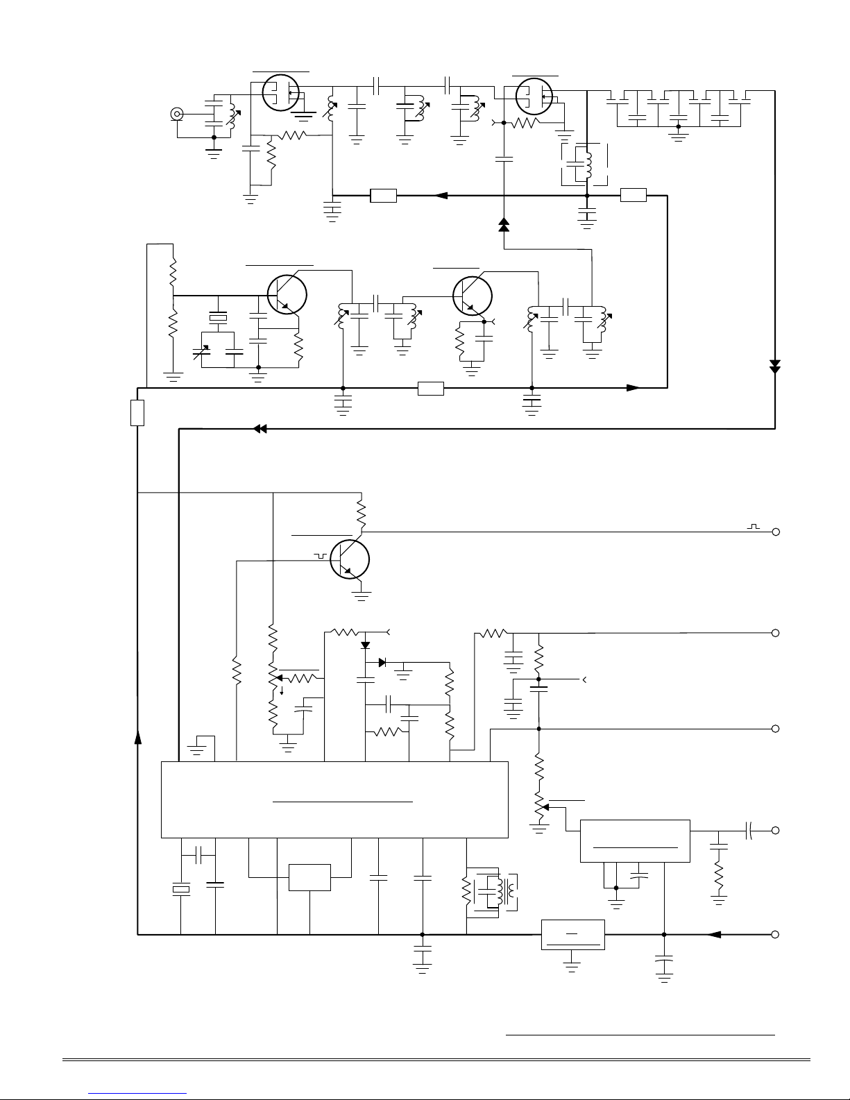
Q1 - RF AMPL
ANT
J1
C1
C2
R4
Y1
R5
C15
Z4
C16
10.7 MHZ
IF SIGNAL
L1
C3
Q3 - OSC/MULT.
C17
C18
R1
R2
C4
R6
C19
TP-4
C10
C23
Q2 - MIXER
OSC INJ
OSC.
TP-1
C24
FL1
FL2 FL3 FL4
R3
C26
C25
L8
C27
C12
L5
Z2
C11
L9
+8VDC
C13 C14
10.7 MHZ
IF SIGNAL
C6
C7
C5
L2
C21
C20
L6
Z1
C22
L3
+8VDC
C8
C9
L4
Q4 - MULT.
L7
R7
Z3
+8VDC
R23
Q5 - INVERTER
R13
SIG. LEVEL
R9
R8
+8VDC
16 15 13
IF INPUT COS SQUELCH GATE NOISE AMPL AF OUT MUTE
OSCILLATOR ----------- MIXER --------------- ---------DETECTOR-------
1 2
C39
C40
Y2
SQUELCH
R10
cw
+
R11
3 4 5 6 7 8
_
C28
U1- IF AMPL/DETECTOR/SQUELCH
FL5
CR1
R12
C29
12 11 10
CR2
C30
R14
C41
TP-2
R15
R16
C31
C42
C43
9 14
R21
R17
C32
C33
R20
L10
R18
C34
R19
VOLUME
3
U3
8-VOLT REG.
FREQ.
TP-3
N/C
1,2
U2 - AUDIO OUTPUT
4 5 8 7
+
_
C35
+
C36
6
_
COS OUTPUT
DISC. OUTPUT
REPEATER AUDIO
SPKR OUT
C38
_
+
C37
R22
+13.6 VDC INPUT
E4
E5
E1
E2
E3
Figure 2. R100 Receiver, Schematic Diagram
Page 7

©
2009
Hamtronics, Inc.; Hilton NY; USA. All rights reserved. Hamtronics is a registered trademark. Revised:
7/28/11
-
Page
7-
PARTS LIST FOR R100
RECEIVER, FOR 140-152
MHZ
(Values for higher frequencies in commercial band shown at end of parts list.
These parts normally are not supplied in
kits except on special order.)
Ref # Value (marking)
C1 15 pf np0
C2 56 pf np0
C3-C4 680pf
C5 15 pf np0
C6 not used *
C7 18 pf np0
C8 not used *
C9 15 pf np0
C10 2 pf np0
C11 .01 uf (103)
C12 8 pf
C13 7 pf
C14 8 pf
C15 Piston trimmer, 2-11.2 pf
C16 39 pf np0
C17-C18 150 pf 1206 chip cap ***
C19 680pf
C20 82 pf np0
C21 2 pf
C22 68 pf np0
C23-C24 680pf
C25 18 pf np0
C26 0.5 pf chip cap ***
C27 20 pf np0
C28 0.47 uf electrolytic
C29 0.15 uf polyester (red)
C30-C31 .001 uf (102, 1nM, or 1nK)
C32-C33 .01 uf (103)
C34 0.15 uf polyester (red)
C35 10 uf electrolytic
C36 47 uf electrolytic
C37 0.15 uf polyester (red)
C38 470 uf electrolytic
C39 68 pf np0
C40 220 pf (221)
C41-C43 0.1 uf monolithic (104)
CR1-CR2 1N4148 ( p/n may not be
marked)
FL1-FL4 10.7 MHz matched xtal
filter set
FL5 455 kHz ceramic filter,
20 kHz bw (blue)
J1 RCA jack
L1-L4 2-1/2 turns (red)
L5 10.7 MHz IF transformer,
p/n 7A-691F or T1005
L6-L7 6-1/2 turns (blue)
L8-L9 2-1/2 turns (red)
L10 455kHz IF transformer
p/n T1003
Q1-Q2 N.E.C. 3SK122 or Philips
BF-988 dual-gate mos fet
(static handling pre-
cautions required)
Q3-Q5 2N5770
R1-R3 100K
R4-R5 15K
R6 680Ω
R7 1K
R8 68K
R9 68K
R10 100K panel-mount pot.
R11 68K
R12 100K
R13 68K
R14 330K
R15 680Ω
R16 4.7k
R17 1K
R18 27K
R19 100K
R20 100K panel-mount pot.
R21 68K
R22 3.3Ω (orn-orn-gold-gold)
R23 27K
U1 MC-3361P IF Ampl/
Det/Squelch
U2 LM380N-8 Audio Amplifier
U3 78L08 Voltage Regulator
Y1 Channel Crystal (see text)
Y2 10.245 MHz, 62 pf,
parallel-resonant IF xtal
Z1-Z4 Ferrite Beads, double long
Note:
* On this band, there is sufficient coupling between pads on the board so no extra capacitance is needed for C6 and C8.
*** Note: disc cap is no longer available in this value. Carefully tack solder surface mount capacitor on
bottom of board. Hold it carefully with
tweezers to avoid dropping it.
➠➠➠➠
Values for 152-165 MHz, for frequency
sensitive parts.
C1 12 pf np0
C2 47 pf np0
C5 12 pf np0
C7 15 pf np0
C9 12 pf np0
C20 68 pf np0
C22 56 pf np0
C25 12 pf np0
C27 18 pf np0
➠➠➠➠
Values for 165-175 MHz, for frequency
sensitive parts.
C1 12 pf np0
C2 47 pf np0
C5 12 pf np0
C7 15 pf np0
C9 12 pf np0
C20 62 pf np0
C22 56 pf np0
C25 12 pf np0
C27 15 pf np0
Page 8

©
2009
Hamtronics, Inc.; Hilton NY; USA. All rights reserved. Hamtronics is a registered trademark. Revised:
7/28/11
-
Page
8-
PARTS LIST FOR HUBBELL
R100 RECEIVER, FOR 72-76
MHZ (NOT USED ANY MORE)
Ref # Value (marking)
C1 33 pf np0
C2 100 pf
C3-C4 680pf
C5 22 pf np0
C6 0.5 pf chip cap ***
C7 27 pf np0
C8 0.5 pf chip cap ***
C9 22 pf np0
C10 2 pf np0
C11 .01 uf (103)
C12 8 pf
C13 7 pf
C14 8 pf
C15 Piston trimmer, 2-11.2 pf
C16 39 pf np0
C17-C18 150 pf 1206 chip cap ***
C19 680pf
C20 150 pf np0 (151)
C21 3 pf
C22 150 pf np0 (151)
C23-C24 680pf
C25 33 pf np0
C26 0.5 pf chip cap ***
C27 39 pf np0
C28 0.47 uf electrolytic
C29 0.15 uf polyester (red)
C30-C31 .001 uf (102, 1nM, or 1nK)
C32-C33 .01 uf (103)
C34 0.15 uf polyester (red)
C35 10 uf electrolytic
C36 47 uf electrolytic
C37 0.15 uf polyester (red)
C38 470 uf electrolytic
C39 68 pf np0
C40 220 pf (221)
C41-C43 0.1 uf monolithic (104)
CR1-CR2 1N4148 ( p/n may not be
marked)
FL1-FL4 see mods
FL5 see mods
J1 RCA jack
L1-L4 6½ turns (blue)
L5 10.7 MHz IF transformer,
p/n 7A-691F or T1005
L6-L9 6½ turns (blue)
L10 455kHz IF transformer
p/n 831-5 or YMC-15002
or T1003
Q1-Q2 N.E.C. 3SK122 or Philips
BF-988 dual-gate mos fet
(static handling pre-
cautions required)
Q3-Q5 2N5770
R1-R3 100K
R4-R5 14K *
R6 680Ω
R7 1K
R8 68K
R9 68K
R10 100K panel-mount pot.
R11 68K
R12 100K
R13 68K
R14 330K
R15 680Ω
R16 4.7K
R17 1K
R18 27K
R19 100K
R20 100K panel-mount pot.
R21 68K
R22 3.3Ω (orn-orn-gold-gold)
R23 27K
U1 MC-3361P IF Ampl/
Det/Squelch
U2 LM380N-8 Audio Amplifier
U3 78L08 Voltage Regulator
Y1 Channel Crystal (see text)
Y2 10.245 MHz, 62 pf,
parallel-resonant IF xtal
Z1-Z4 Ferrite Beads, double long
*** Note: disc cap is no longer available in this value. Carefully tack solder surface mount capacitor on
bottom of board. Hold it carefully with
tweezers to avoid dropping it.
DATA FILTER MODS.
This column provides information on
modifications for using this receiver for fsk
data reception. It is intended to give specific
information on parts.
PARTS INCLUDED.
1 ea. 10.7MA ceramic filter*
1 ea. LT455B ceramic filter
*Note: The crystal filters normally used in
a receiver kit are not supplied when this option is ordered.
RECEIVER MODIFICATIONS.
If you are building a kit, please mark the
parts list with the following changes before
beginning construction and use the attached
parts location view in place of the one which
comes with the kit. If you ordered a wired
unit, these changes have already been made.
a. Remove or do not install regular i-f filters FL1-FL4 and capacitors between sections
of the crystal filter, which are C12-C14 for the
R100, C11-C13 for the R451, or C41-C43 for
the R302 or R305 Receivers.
b. In positions for FL1, FL2, and FL3, install
pieces of bus wire (lead clippings from some
components) between the two end holes
(don't use center ground hole). Make the
jumpers as short as possible to minimize inductance.
c. Install "10.7MA" ceramic filter (small 3
lead device) in position FL4. You may have to
use something like a dental pick to enlarge the
holes slightly, but don’t remove the plating
within the hole.
d. Install LT455B ceramic filter in position FL5.
Page 9

©
2009
Hamtronics, Inc.; Hilton NY; USA. All rights reserved. Hamtronics is a registered trademark. Revised:
7/28/11
-
Page
9-
PARTS LIST FOR REGULAR
R100 RECEIVER, FOR 72-76
MHZ
Ref # Value (marking)
C1 33 pf np0
C2 100 pf
C3-C4 680pf
C5 22 pf np0
C6 0.5 pf chip cap ***
C7 27 pf np0
C8 0.5 pf chip cap ***
C9 22 pf np0
C10 2 pf np0
C11 .01 uf (103)
C12 8 pf
C13 7 pf
C14 8 pf
C15 Piston trimmer, 2-11.2 pf
C16 39 pf np0
C17-C18 150 pf 1206 chip cap ***
C19 680pf
C20 150 pf np0 (151)
C21 3 pf
C22 150 pf np0 (151)
C23-C24 680pf
C25 33 pf np0
C26 0.5 pf chip cap ***
C27 39 pf np0
C28 0.47 uf electrolytic
C29 0.15 uf polyester (red)
C30-C31 .001 uf (102, 1nM, or 1nK)
C32-C33 .01 uf (103)
C34 0.15 uf polyester (red)
C35 10 uf electrolytic
C36 47 uf electrolytic
C37 0.15 uf polyester (red)
C38 470 uf electrolytic
C39 68 pf np0
C40 220 pf (221)
C41-C43 0.1 uf monolithic (104)
CR1-CR2 1N4148 ( p/n may not be
marked)
FL1-FL4 10.7 MHz matched xtal
filter set
FL5 455 kHz ceramic filter,
20 kHz bw (blue)
J1 RCA jack
L1-L4 6½ turns (blue)
L5 10.7 MHz IF transformer,
p/n 7A-691F or T1005
L6-L9 6½ turns (blue)
L10 455kHz IF transformer
p/n 831-5 or YMC-15002
or T1003
Q1-Q2 N.E.C. 3SK122 or Philips
BF-988 dual-gate mos fet
(static handling pre-
cautions required)
Q3-Q5 2N5770
R1-R3 100K
R4-R5 15K
R6 680Ω
R7 1K
R8 68K
R9 68K
R10 100K panel-mount pot.
R11 68K
R12 100K
R13 68K
R14 330K
R15 680Ω
R16 4.7K
R17 1K
R18 27K
R19 100K
R20 100K panel-mount pot.
R21 68K
R22 3.3Ω (orn-orn-gold-gold)
R23 27K
U1 MC-3361P IF Ampl/
Det/Squelch
U2 LM380N-8 Audio Amplifier
U3 78L08 Voltage Regulator
Y1 Channel Crystal (see text)
Y2 10.245 MHz, 62 pf,
parallel-resonant IF xtal
Z1-Z4 Ferrite Beads, double long
*** Note: disc cap is no longer available in this value. Carefully tack solder surface mount capacitor on
bottom of board. Hold it carefully with
tweezers to avoid dropping it.
Page 10

©
2009
Hamtronics, Inc.; Hilton NY; USA. All rights reserved. Hamtronics is a registered trademark. Revised:
7/28/11
-
Page
10-
PARTS LIST FOR R100
RECEIVER, FOR 216-225
MHZ
Ref # Value (marking)
C1 3 pf np0
C2 not used
C3-C4 680pf
C5 5 pf np0
C6 not used *
C7 6 pf np0
C8 not used *
C9 0.5 pf chip cap ***
C10 6 pf np0
C11 .01 uf (103)
C12 8 pf
C13 7 pf
C14 8 pf
C15 Piston trimmer, 2-11.2 pf
C16 39 pf np0
C17-C18 150 pf 1206 chip cap ***
C19 680pf
C20 62 pf np0
C21 1 pf
C22 56 pf np0
C23-C24 100 pf (101)
C25 4 pf np0
C26 not used
C27 6 pf np0
C28 0.47 uf electrolytic
C29 0.15 uf polyester (red)
C30-C31 .001 uf (102, 1nM, or 1nK)
C32-C33 .01 uf (103)
C34 0.15 uf polyester (red)
C35 10 uf electrolytic
C36 47 uf electrolytic
C37 0.15 uf polyester (red)
C38 470 uf electrolytic
C39 68 pf np0
C40 220 pf (221)
C41-C43 0.1 uf monolithic (104)
CR1-CR2 1N4148 ( p/n may not be
marked)
FL1-FL4 10.7 MHz matched xtal
filter set
FL5 455 kHz ceramic filter,
20 kHz bw
J1 RCA jack
L1-L4 2-1/2 turns (red)
L5 10.7 MHz IF transformer,
p/n 7A-691F or T1005
L6-L7 6-1/2 turns (blue)
L8-L9 2-1/2 turns (red)
L10 455kHz IF transformer
p/n 831-5 or YMC-15002
or T1003
Q1-Q2 N.E.C. 3SK122 or Philips
BF-988 dual-gate mos fet
(static handling pre-
cautions required)
Q3-Q5 2N5770
R1-R3 100K
R4-R5 15K
R6 680Ω
R7 1K
R8 68K
R9 68K
R10 100K panel-mount pot.
R11 68K
R12 100K
R13 68K
R14 330K
R15 680Ω
R16 4.7K
R17 1K
R18 27K
R19 100K
R20 100K panel-mount pot.
R21 68K
R22 3.3Ω (orn-orn-gold-gold)
R23 27K
U1 MC-3361P IF Ampl/
Det/Squelch
U2 LM380N-8 Audio Amplifier
U3 78L08 Voltage Regulator
Y1 Channel Crystal (see text)
Y2 10.245 MHz, 62 pf,
parallel-resonant IF xtal
Z1-Z4 Ferrite Beads, double long
Note:
* On this band, there is sufficient coupling between pads on the board so no extra capacitance is needed for C6 and C8.
*** Note: disc cap is no longer available in this value. Carefully tack solder surface mount capacitor on
bottom of board. Hold it carefully with
tweezers to avoid dropping it.
Page 11
©
2009
Hamtronics, Inc.; Hilton NY; USA. All rights reserved. Hamtronics is a registered trademark. Revised:
7/28/11
-
Page
11-
PARTS LIST FOR R100
RECEIVER, FOR 46-54 MHZ
Ref # Value (marking)
C1 82 pf np0
C2 150 pf np0 (151)
C3-C4 .001 uf (102, 1nM, or 1nK)
C5 56 pf np0
C6 1 pf
C7 62 pf np0
C8 1 pf
C9 56 pf np0
C10 6 pf np0
C11 .01 uf (103)
C12 8 pf
C13 7 pf
C14 8 pf
C15 Piston trimmer, 2-11.2 pf
C16 39 pf np0
C17-C18 150 pf 1206 chip cap ***
C19 .001 uf (102, 1nM, or 1nK)
C20 82 pf np0
C21 2 pf
C22 82 pf np0
C23 not used
C24 .001 uf (102, 1nM, or 1nK)
C25 82 pf np0
C26 2 pf
C27 82 pf np0
C28 0.47 uf electrolytic
C29 0.15 uf polyester (red)
C30-C31 .001 uf (102, 1nM, or 1nK)
C32-C33 .01 uf (103)
C34 0.15 uf polyester (red)
C35 10 uf electrolytic
C36 47 uf electrolytic
C37 0.15 uf polyester (red)
C38 470 uf electrolytic
C39 68 pf np0
C40 220 pf (221)
C41-C43 0.1 uf monolithic (104)
C44 2 pf
CR1-CR2 1N4148 ( p/n may not be
marked)
FL1-FL4 10.7 MHz matched xtal
filter set
FL5 455 kHz ceramic filter,
20 kHz bw (blue)
J1 RCA jack
L1-L4 6½ tunrs (blue)
L5 10.7 MHz IF transformer,
p/n 7A-691F or T1005
L6-L9 6½ turns (blue)
L10 455kHz IF transformer
p/n 831-5 or YMC-15002
or T1003
Q1-Q2 N.E.C. 3SK122 or Philips
BF-988 dual-gate mos fet
(static handling pre-
cautions required)
Q3 2N5770
Q4 not used
Q5 2N5770
R1-R3 100K
R4-R5 15K
R6 680Ω
R7 not used
R8 68K
R9 68K
R10 100K panel-mount pot.
R11 68K
R12 100K
R13 68K
R14 330K
R15 680Ω
R16 4.7K
R17 1K
R18 27K
R19 100K
R20 100K panel-mount pot.
R21 68K
R22 3.3Ω (orn-orn-gold-gold)
R23 27K
U1 MC-3361P IF Ampl/
Det/Squelch
U2 LM380N-8 Audio Amplifier
U3 78L08 Voltage Regulator
Y1 Channel Crystal (see text)
Y2 10.245 MHz, 62 pf,
parallel-resonant IF xtal
Z1-Z4 Ferrite Beads, double long
*** Note: disc cap is no longer available in this value. Carefully tack solder surface mount capacitor on
bottom of board. Hold it carefully with
tweezers to avoid dropping it.
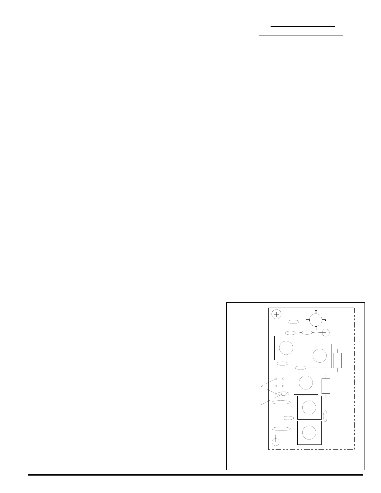
THESE 5 HOLES
NOT USED
C44 INSTALLED
IN PLACE OF Q4
BASE-COLLECTOR
DETAIL OF LEFT-REAR CORNER OF RECEIVER
SHOWING COMPONENT CHANGES FOR THIS MODEL
➠
Note the following
changes for this model:
1. R7 and C23 are not used. Q4 is replaced with C44, installed where the
base and collector leads of Q4 would
normally go. (See detail below.)
2. When tuning the oscillator, a change
in procedure is required because this
frequency scheme does not use a multiplier stage. L6-L9 are all simply
peaked for maximum signal sensitivity.
Skip alignment procedure step (c). In
step (g), alternately peak all four coils,
L6-L9, for maximum as stated for L8L9.
R5
C22
C20
C27
C26
L9
C25
C21
Q3
C24
C10
L8
Q2
R3
L5
Z2
Z3
L7
L6
C43
C19
 Loading...