

Page 1

HAMTRONICS® LPA 2-15R, LPA 3-15R, & LPA 6-25R
REPEATER POWER AMPLIFIERS:
ASSEMBLY, INSTALLATION, & MAINTENANCE
GENERAL INFORMATION.
The Power Amplifier is a class C
device designed to be installed as an
integral part of a transmitter enclosure in a repeater installation with a
2 Watt exciter module.
This PA comes in models for several vhf bands and power levels as
follows:
LPA 2-15R 140-175 MHz 17-20W
LPA 3-15R 213-233 MHz 17-23W
LPA 6-25R 50-54 MHz 20-25W
The Power Amplifier operates on
+13.6 Vdc at about 4 to 5 Amp, depending on output power level. It has
a 50-ohm input and output impedance and is designed for continuous
duty.
A low-pass filter reduces harmonic
output to very low levels. The unit is
FCC type accepted for commercial
operation in the 150-175 MHz band.
CONSTRUCTION.
General.
Most of the pertinent construction
details are given in the component location and schematic diagrams and
parts list.
All parts are tack soldered to the
pc board; so it is necessary to cut and
form leads so that they seat properly
on the board and be sure to keep
leads as short and direct as possible.
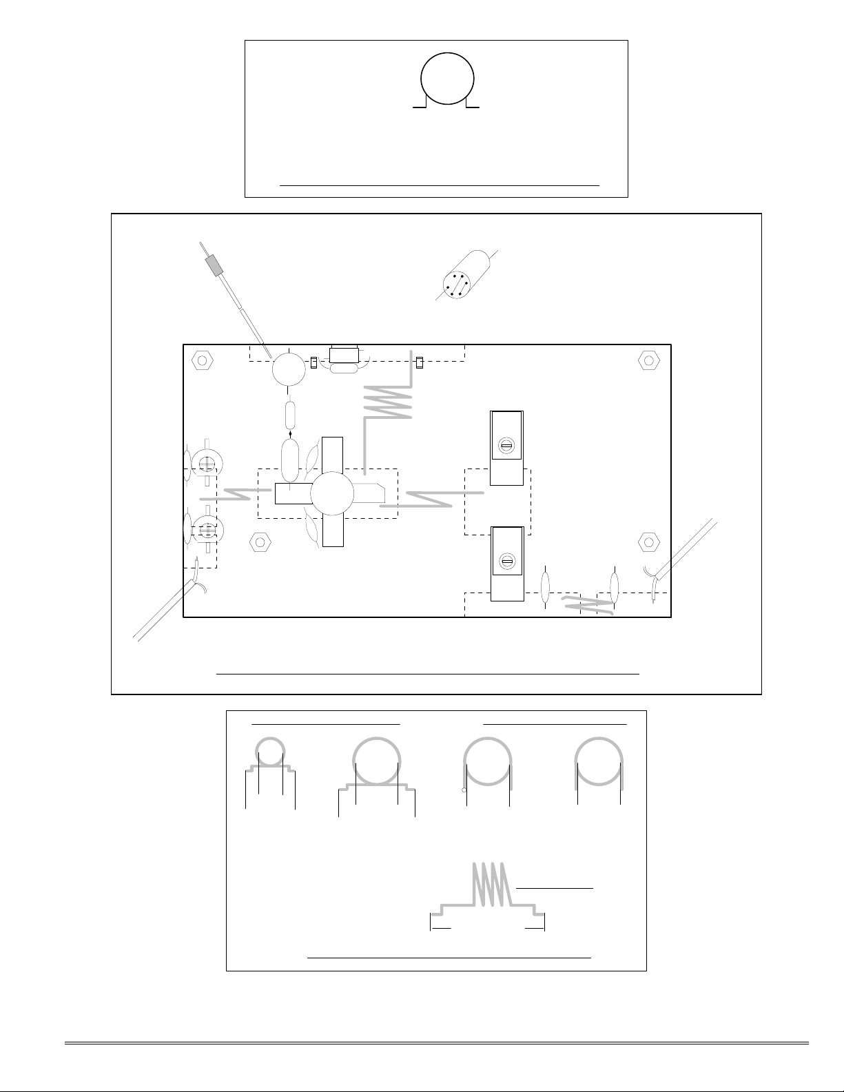
This is especially true of the disc capacitors. Figure 1 shows how to trim
and form the leads of capacitors.
PCB, Transistor, and Heatsinking.
This series of power amplifiers is
designed to be mounted in an rf tight
enclosure with the exciter in such
applications as our REP-200 Repeater. The unit is supplied less
heatsink and mounting hardware,
since the enclosure acts as a heatsink
and the hardware normally is provided with the repeater kit.
If you have purchased the PA for
some other use or mounting method,
it is important to assemble and use
the unit as we do in the repeater to
avoid damage to the transistor by
pulling the leads off the ceramic case.
The pa is designed to have the thickness of a standard 4-40 nut (about
0.100 inch) as a spacer between the
pc board and the chassis on which
the transistor is mounted.
a. If you are supplying your own
enclosure, mark and drill four clearance holes for mounting the board
with 4-40 screws and one 8-32 clearance hole to mount the transistor in
the center of the cutout in the board.
The latter hole must be close to the
diameter of the xstr stud to provide
maximum surface for the shoulder of
the transistor to contact the chassis
for heatsinking; so do not make this
hole oversize.
b. Install four 4-40 x 3/8 inch
screws from the bottom of the enclosure and secure with 4-40 nuts.
c. Set pc board over screws, and
align so cutout for transistor is centered over hole in enclosure. Secure
the board with 4-40 nuts and lockwashers.
d. Carefully open the package of
heatsink compound with scissors.
Use a toothpick or small piece of wire
to apply a small amount of compound
to the shoulder of the transistor
where it contacts the heatsink.
e. Set the transistor in place, and
orient the notched collector lead to
the right as shown. Secure transistor
with #8 lockwasher and 8-32 nut. Do
not overtighten nut; tighten only to
the point of being snug. Hold transistor leads with fingers to prevent rotation. If leads still rotate, you are
probably applying too much torque.
Note: Since heatsink compound is
used, it is unnecessary to use a lot of
torque, which could break the stud.
f. Form the transistor leads down
against the board. Then, tack solder
them to the foil, using sufficient solder so that a bond is formed under
the full length of the leads. Note that
other parts will be soldered on top of
the base and collector leads; so it
helps to thoroughly flood those leads
with solder.
Installing Capacitors.
a. Solder variable mica capacitors
C8 and C9 to the board in the exact
positions shown in figure 2. Mount
the capacitors oriented as shown so
the rotor screw is connected to the
proper side of the circuit (as shown in
fig. 2).
b. Bend the leads of C2 and C3
gently at a 90° angle, and solder them
as shown. Make sure the round end
of C2 goes to ground.
c. Form the leads of C1 and C15
(if used) close to the body, as shown
in figure 1, and tack solder on the
board.
d. Tack solder C4-C5 and C6-C7
(if used) as shown, bending the leads
at right angles, and keeping them as
short as possible, as shown in figure
1. It is important to angle the capacitors as shown in figure 2 and position
them as close as possible to the body
of the transistor. The idea is to connect them electrically as close as possible to the emitter and base
terminals or the emitter and collector
terminals. In fact, they should be
soldered on top of those leads.
e. Tack solder C13 and C14 as
shown, bending the leads at right angles, and keeping them as short as
possible. Position the capacitors as
shown in figure 2.
f. Tack solder chip capacitors C10
and C11 as follows. Position the capacitors as shown in figure 2 or 5.
They are installed between the B+
pad and ground. Use small tweezers
to handle them. Be careful not to
drop them; they are difficult to find.
Since they have no markings, be sure
to leave them in the package until installled so you can tell the values
apart.
Apply a little solder to the B+ pads
adjacent to where each capacitor will
be positioned. Do not apply solder to
the ground plane yet.
Pick up one capacitor at a time.
Set the capacitor in place. Then, heat
the solder on the pc board pad, and
allow the solder to bond to the electrode on the capacitor. When the
solder melts, the capacitor will seat
down on the board in the molten solder. It is essential that this process
be done relatively quickly so the solder doesn't oxidize and so there is
still a little flux left where the capacitor electrode sits.
After one end of each capacitor is
soldered and the positions have been
checked, solder the ground plane end
of each capacitor.
g. Tack solder electrolytic capacitor C12. Bend the leads at right angles, and observe polarity.
©1999 Hamtronics, Inc.; Hilton NY; USA. All rights reserved. Hamtronics is a registered trademark. Revised: 12/11/02 - Page 1 -
Page 2

RF Choke, Ferrite Beads, and Resistors.
a. Ferrite choke Z2 is threaded
with 2½ turns of #22 bus wire, as
shown in the detail, by feeding the
wire through opposite holes and pulling tight. One hole will not be used.
Be sure to wind
around through the holes as shown.
Do not thread the wire through in a
zig-zag fashion. The choke is
mounted flat against the pc board,
and the leads are tack soldered to the
board.
b. Install resistor R2 across Z2 as
shown.
c. Cut the bus wire off the ferrite
bead close to one end of the bead and
discard the leads.
d. The following procedure installs a power lead of the proper
length for our repeater. If you have a
different installation, you can do
something similar. Cut a 3 inch
length of red hookup wire. Strip one
end ¼ inch and the other end 5/8
inch. Tack solder the ¼inch end to
the pc board power trace as shown.
Be careful to apply fresh solder over
the wire so you don't get a cold solder
joint from simply reheating solder already on the trace. Slide the ferrite
bead over the long end, and bend the
wire at a slight angle to hold the bead
in place until you solder the lead to
the feedthrough capacitor in the repeater.
e. Twist together and tack solder
one lead each of rf choke L2 and resistor R1. Trim the other lead of each
part to about ¼ inch and form down
to reach the board. Then, tack solder
these leads to the board as shown,
with the lead of L2 to the pad area for
the base of the transistor and the
lead of R1 to the ground plane.
f. For 220 MHz, install R3 and
R4 with very short leads exactly as
shown. Tack solder to traces and
ground plane.
the wire around and
Coil Forming and Placement.
Figures 2 & 3 and 5 & 6 show exactly how coils are formed for the 144
and 220 MHz versions of the PA, respectively. If you have the 6 meter
version, separate drawings are provided for that unit.
You need to form the coils exactly
as specified, using #18 bus wire supplied. Tack solder them to the board
in the positions shown.
Any rod of the proper diameter
(such as the shank of a drill bit) can
be used as a forming tool for coil
winding. It is important that they not
only be wound the proper inside diameter but that the leads be the
proper length. Any extra lead length
adds to the inductance and will affect
performance. You don't need to be
super precise, but do form them to
resemble the detailed drawings as
closely as you can.
Remember that the finished coils
should fit on the pc traces as shown;
so that will help you check that you
formed the coils properly.
For 144 MHz, the coils are all either 1/8 or 1/4 inch inside diameter.
Spacing between turns of the coils
should be minimal, with turns separated just enough to prevent shorting
together.
L1 is 1/8 inch i.d. and 1-1/4
turns. The feet are formed just so the
bottom wire of the coil doesn't short
to the ground plane. The feet should
be only about 1/16 inch high. The
other three coils are 1/4 inch i.d. L3
is 1-1/4 turns. L4 is 3-3/4 turns.
L5 is 1-3/4 turns.
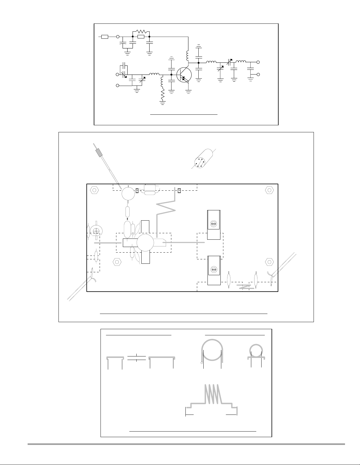
For 220 MHz, L1 and L3 actually
are jumpers formed with legs so that
the top of the jumpers are 1/8 inch
above the board, as shown in figure
6. L4 is 1-3/4 turns on 1/4 inch i.d.
L5 is 1-1/4 turns on 1/8 inch i.d.
Spacing between turns of the coils
should be minimal, with turns separated just enough to prevent shorting
together. The feet are formed on L5
just so the bottom wire of the coil
doesn't short to the ground plane.
(Note that L1 and L3 are shown in
figure 5 at a smaller scale than the
rest of the coils.)
Inspection.
This completes assembly. Check
to be sure all parts are installed according to parts list. Look for any
short circuits or bad solder joints. RF
power transistors are expensive to replace; so now is the time to find problems, before power is applied.
RF INPUT/OUTPUT CONNECTIONS.
The input and output connections
are made with RG-174/u 50-ohm
coax cable connected to the appropriate input and output pads and
ground plane of the pc board.
The following lengths assume that
PA will be installed in REP-200 Repeater. The input cable should be 5½
inches long and the output cable
should be 3 inches long, measured
before stripping the ends.
Connect cables by stripping and
tack-soldering to board as illustrated.
Note that stripped length of coax is
inductive; so keep pigtail leads as
short as possible.
Connect the shields by pretinning
the shield and then tack soldering
the end which contacts the board.
Avoid melting polyethylene insulation
on cable by pretinning board and cable and then tacking them together
quickly.
POWER CONNECTIONS.
+13.6Vdc should be connected to
the B+ pad at the top of the pc board.
When installed in an REP-200 Repeater, a hookup wire should be attached to the B+ pad as shown, using
a ferrite bead on the far end, which
attaches to the feedthrough capacitor
in the PA compartment. The ground
return normally is connected to the
pc board through the mounting
hardware.
The cable should be #18 or larger
wire to minimize voltage drop. A 6
Amp, quick acting fuse should be
connected in the positive supply line
for protection.
A well regulated power supply
should be used. Current drain of the
PA at full output is about 4 to 5 Amp,
sometimes slightly higher (but no
more than 6 Amp), depending on
power level.
Note that the output capability of
the PA drops rapidly as the voltage is
reduced below 13.6Vdc; therefore,
you should try to use a power source
of sufficient voltage and minimize cable losses so that you have full B+
available at the PA.
CAUTIONS TO PROTECT TRANSISTORS.
Because it is so easy to damage rf
power transistors in the field due to
accidents and abuse, transistor
manufacturers do not provide any
warranty to cover replacements once
a transistor is installed in the unit.
They test them thoroughly at the factory because they are expensive
parts. Therefore, they do not honor
claims that "the transistor must have
been bad from the factory". / For
your protection, please be sure to observe the following precautions:
1. Sometimes, transistors may be
destroyed by parasitic oscillations occurring during tuning because of the
extremes of capacitor settings, or due
to accidental shorting of components.
To protect against such damage as
©1999 Hamtronics, Inc.; Hilton NY; USA. All rights reserved. Hamtronics is a registered trademark. Revised: 12/11/02 - Page 2 -
Page 3

much as possible, turn power supply
voltage down to about 10 Volts when
you first apply power until the unit is
tuned. Then, turn up to full 13.6Vdc.
Of course, final tuning should be
done at full 13.6V.
2. Never exceed 13.6Vdc, as even
a small over-voltage causes strain on
transistors because of additional
heat.
3. Be sure you have a low impedance connection to the power supply,
i.e., short, heavy cable.
4. Do not attempt to operate PA
until exciter has been properly
aligned by itself, operating into a
50-ohm load.
ALIGNMENT.
Alignment is very simple. Connect
the input to an exciter which has already been tuned into a 50-ohm
dummy load. Connect the output to
a 50-ohm load of sufficient power rating. Use an in-line power meter, or
monitor output with a dc voltmeter
connected to rf detector test point pad
on pc board.
Preset variable capacitors as follows if this is the first time tuning
from a kit; otherwise, they should be
left where previously tuned. The
large mica variable capacitors should
be screwed down tight and then
backed off about three turns. The
small ceramic variable capacitors
should be rotated 90° from where
they are set from the factory.
Apply B+ and moderate rf drive.
Alternately tune the four variable capacitors for maximum output. Continue increasing drive slightly and
repeaking capacitors until maximum
output is achieved and all interactions between capacitors are worked
out.
Note: Do not retune exciter with PA
connected. Once the exciter is tuned
Ω
into a 50
tuned again. Tuning the input of the
PA takes care of matching the PA to
the exciter.
With 13.6Vdc power applied and
2W drive, the 144 MHz unit should
put out about 17-20W or 25-30W,
depending on model, the 220 MHz
unit should put out about 17-23W,
and the 50 MHz unit should put out
about 20-25W. Current drain should
be about 4-5 Amp.
To minimize stress on the transistor, avoid running the pa over these
maximum levels. A good way to re-
load, it should never be
duce the output power and the current drain is to tighten loading
capacitor C9 slightly and repeaking
tuning capacitor C8. It is usually
possible to reduce both the power
level and the current drain that way.
Watch both meters while tuning to be
sure that is what is happening.
You can tell if the transistor is
overheating by watching the output
power and current drain as the unit
heats up. Neither should change
much. If the output power sags by
more than a few watts as the transistor heats up, there is insufficient
heatsinking. Either the heatsink is
too small or the thermal interface between the transistor and heatsink is
deficient. There should be heatsink
compound between the two surfaces
and the nut on the transistor stud
should be tight (but not strained to
the breaking point).
OPERATION.
Operation is quite simple. B+ can
be applied all the time if desired.
Merely apply an rf signal to the PA
when you want to transmit.
TROUBLESHOOTING.
Since the unit has only one simple
amplifier stage, there isn't much
which can go wrong. The circuitry is
straightforward. The first things to
suspect should there be no output
are shorted coax cables or incorrect
or shorted pc board component connections.
Should it be necessary to replace
rf power transistor Q1, be sure to use
an exact replacement. There are
other transistors rated at similar output level, but they may have lower
gain or different impedance characteristics.
To replace the transistor, carefully
peel each lead away from the pc
board while melting the solder. Then,
remove the mounting hardware and
gently push the old transistor out of
the heatsink. Clean all the old solder
off the pc board and remove the old
heatsink compound. Add new heatsink compound, and install new transistor with collector lead in correct
location. Carefully tighten nut on
transistor without over-torquing.
Then, flatten leads against the board,
and sweat solder them to the board.
Remember to resolder any components removed for access to the transistor leads.
/ A word about relay coils. Any
relay coil connected to the same B+
line as solid state equipment should
have a reverse diode connected
across it to absorb the inductive
kickback which occurs when the coil
is de-energized. Relay coils and similar inductors can cause transients up
to several hundred volts. This is the
most common problem related to
damaged semiconductors. You
should also be sure that your power
supply does not have an inductive
surge when you turn it on or off. If in
doubt, borrow an oscilloscope and
watch the B+ line when you turn the
switch on and off.
PARTS LIST.
(See separate sheet for 6M version.)
Ref Desig Description
C1 39 pf disc capacitor
[22 pf for 220 MHz band]
C2 20 pf (pink) ceramic var.
C3 20 pf (pink) ceramic var.
[.001 disc cap for 220 MHz
band, marked 102 or 1n]
C4-C5 For LPA 2-15R:
47pf for C4, none for C5
[For 220 MHz: 110 pf disc
marked "111"]
C6-C7 not used
C8-C9 mica variable marked
"703"
C10 .001 uf chip capacitor
C11 .047 uf chip capacitor
C12 47 uf electrolytic cap
C13-C14 56 pf disc capacitor
[33 pf for 220 MHz band]
C15 5pf disc capacitor
[not used on 220 MHz]
L1, L3-L5 wind per text
L2 0.22 uh rf choke marked
red-red-silver-red
Q1 2N6081 (Motorola) or
BLY-88C (Philips)
[BLW-40 for 220 band]
R1 3.3Ω, ¼W resistor
R2 10Ω, ¼W resistor
R3, R4 27Ω, ¼W resistor
Z1 Ferrite bead over B+ lead
Z2 2½ turn ferrite choke
Chip Capacitors taped here for kit:
1 ea .001 uF ------
1 ea .047 uF ------
©1999 Hamtronics, Inc.; Hilton NY; USA. All rights reserved. Hamtronics is a registered trademark. Revised: 12/11/02 - Page 3 -
Page 4
s
+13.6VDC IN
STRIP WIRE 5/8" &
INSTALL BEAD Z1
VERY SHORT LEADS
ON DISC CAPACITORS
Figure 1. Lead Trimming and Forming Detail
C15
RF INPUT
FERRITE CHOKE Z2, SEE TEXT
Z2
R2
C10
L4
C8
C1 C2
3" RED WIRE
+
C12
_
C11
R1
C4
L2
L1
Q1
L3
C3
C5
C9
C13
Figure 2. LPA 2-15R for 144 MHz, Component Location Diagram
FRONT VIEWS
L1
L4
RF OUTPUT
C14
L5
L5L3
1/8 IN. I.D.
5/8 IN. END-END
1/4 IN. I.D.
7/8 IN. END-END
1/4 IN. I.D. 1/4 IN. I.D.
L4 RIGHT SIDE VIEW
1-3/8 IN. END-END
Figure 3. Coil Winding Details for 144 MHz
©1999 Hamtronics, Inc.; Hilton NY; USA. All rights reserved. Hamtronics is a registered trademark. Revised: 12/11/02 - Page 4 -
Page 5
2
O
R
+
Z1
RF INPUT
C12
C15
C3
_
C11
C1 C2
Z2
C10
L4
Q1
C4
L1
L2
C5
R1
Figure 4. Schematic Diagram
C6
C7
C9
C13
L5
RF OUTPUT
C14
L3
C8
+13.6VDC IN
STRIP WIRE 5/8" &
INSTALL BEAD Z1
C1 C2
C3
3" RED WIRE
R1
L2
L1
+
C12
_
R4
R3
C11
C4
Q1
C5
FERRITE CHOKE Z2, SEE TEXT
Z2
R2
C10
L4
L3
C8
C9
C13
RF OUTPUT
C14
L5
RF INPUT
Figure 5. LPA 3-15R for 220 MHz, Component Location Diagram
FR
NT VIEWS
L1
1/2 IN.
1/8 IN. HIGH
3/4 IN.
L4
L3
1/4 IN. I.D.
L4 RIGHT SIDE VIEW
1-3/8 IN END-END
L5
1/8 IN. I.D.
Figure 6. Coil Winding Details for 220 MHz
©1999 Hamtronics, Inc.; Hilton NY; USA. All rights reserved. Hamtronics is a registered trademark. Revised: 12/11/02 - Page 5 -
 Loading...