

Page 1

-
HAMTRONICS LPA 4-35 UHF LINEAR POWER AMPLIFIER
CONSTRUCTION, ALIGNMENT, & OPERATION INSTRUCTIONS
GENERAL INFORMATION.
The LPA 4-35 is designed to be
used either as a linear amplifier with a
transmitting converter or as a class C
amplifier with an fm exciter in the
420-450 MHz band. It is a new
version of the popular LPA 4-30
Amplifier.
As a linear amplifier, it will take a
1-1/2 Watt p.e.p. output from a
transmitting converter, such as the
XV4, and provide 30-35W output. In
class-C operation, it will amplify the
2W output from an exciter, such as
the TA451, to provide 35-40W output.
It is designed to match a 50Ω input
and output impedance, and it is rated
for continuous duty.
In linear mode, the LPA 4-35 may
be used for any mode of operation,
including ssb, am, cw, atv, and fm.
For exclusive use on modes such as
fm and cw, where linearity is not
required, the bias circuits can be
modified for class-C (actually between
class-B and class-C) for more
efficiency and it can be driven to
slightly higher output.
The unit operates on 13.6 Vdc at
8-10 Amp peak. It was designed for
the 420-450 MHz ham band, but it
may also be tuned to other nearby
frequencies with reduced efficiency. It
has a 10 MHz bandwidth without
retuning; so it is ideal for TV
transmissions.
CIRCUIT DESCRIPTION.
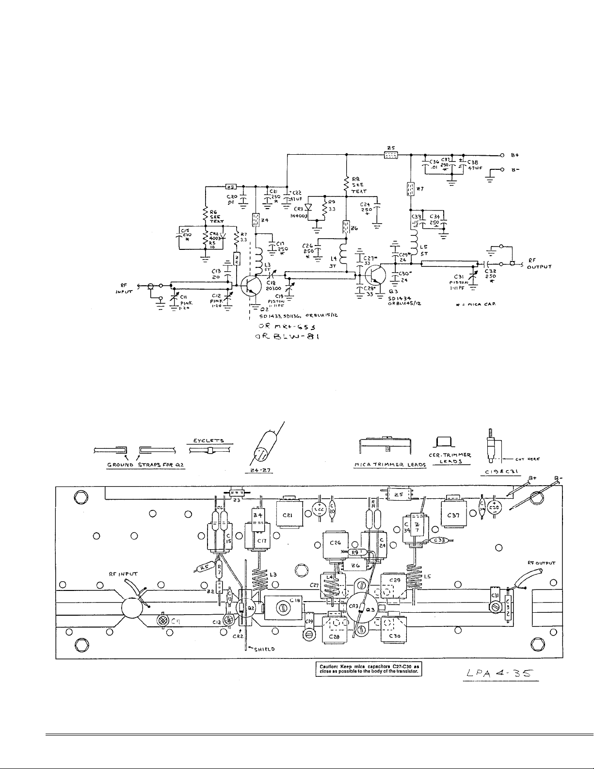
Refer to the schematic diagram.
Amplifier transistors Q2 and Q3 are
the new generation, high gain, emitter
ballasted rf power transistors. They
are operated well below their full
capability to remain in the linear
range. Impedance matching is done
with high efficiency printed
transmission lines (strip lines).
Note that what used to be a predriver stage on the pc board is no
longer needed with the premium high
gain transistors available now.
Therefore, only two stages are used,
providing better stability and linearity
as well as reduced complexity and
cost.
The transistors are normally
biased slightly above class-B for
linearity. However, when the unit is
to be used only for fm or cw, greater
efficiency and power output is
obtained by running the driver stage
just on the edge of conduction in
class-B and the output stage in classC (no bias).
Silicon diodes CR2 and CR3 are
thermally coupled to the transistor
cases to regulate the base bias
according to the transistor
temperature for a stable idle current
over a wide temperature range to
prevent thermal runaway. As the
transistors warm up, they tend to
conduct more; but the diodes reduce
the bias accordingly to counteract the
drift in idle current.
CONSTRUCTION.
Most of the pertinent construction
details are given on the component location and schematic diagrams and in
the parts list. Following are details of
special procedures and techniques
and a general construction sequence
to be used. Note that all parts are
tack soldered to the pc board; so it is
necessary to cut and form leads so
that they seat properly on the board.
a. Lay the pc board on a box or
hold in a vise horizontally with the
etched side of the board up. Using a
sharp pick or any other convenient
tool, pick up eyelets and place in the
small holes. The heads of the eyelets
must rest flat against the foil on the
etched side of the board. then, using
a small amount of solder, solder the
heads of the eyelets to the foil. The
eyelets connect the pc board front and
rear foils together at critical locations.
Be sure to solder all around the heads
of the eyelets to provide low
impedance.
b. Turn the pc board over, and
solder the other side of the eyelets to
the ground plane. Be sure all are
soldered, and check to make sure
none have slipped back through the
other side. If so, heat eyelet flange on
top side of board until solder on both
sides melts, and push eyelet gently
back in place. Note that it is
especially important that the 8 eyelets
under the emitter leads of Q3 (see
diagram) are properly seated and that
no solder blobs protrude above eyelet
heads. This is to prevent stress on
the transistor leads when it is installed later.
c. Locate the thin brass strip
stock. Use scissors to cut two pieces
each 5/8 inch long. Form them with
pliers to fit pc board as shown in the
detail above the component location
diagram. The purpose of these straps
is to provide a low inductance
connection between the emitter leads
of Q2 and the bottom side ground
plane foil. The strap should be bent
so that it fits tightly, with about 1/4
inch on the top and bottom of the
board. Refer to component location
diagram to determine positions of the
emitter leads of Q2; these are the
leads under the shield shown on the
diagram. Tack solder the straps in
place on the bottom of the board only.
The straps will not be soldered to the
top of the board until after Q2 is
installed.
d. Position the heat sink on the
bench, oriented so holes align with the
pc board as shown in the diagram.
Note that the heatsink is used for
several products; so there will be extra
holes on the pc board which are not
used in this model. Place five #6 x
1/16 inch thick flat washers over the
mounting holes. Carefully set the pc
board over the washers, positioning as
shown in the diagram. Secure the
board to the heatsink with five 6-32 x
3/8 inch thread cutting screws,
making sure that the washers stay in
place and that transistor holes are
aligned over heatsink holes.
Note: If you are building the pa for
class-C operation (fm or cw) instead of
linear mode, refer to separate
paragraph on differences later in this
text before beginning construction.
e. Next, mount the transistors as
follows. Make sure you know which
lead is the collector. Carefully open
the package of heatsink compound
with scissors. Apply it sparingly with
a small piece of wire or a toothpick,
etc. It is necessary only to use
enough compound to make a smooth
thermal surface between the heatsink
and transistor. Using too much only
makes a mess. Be sure not to over
tighten the nut on the transistor stud;
the gold-plated brass stud could
break.
f. Unpack the stud-mount
transistor used for Q2. Use scissors
to trim each lead to about 1/4 inch.
Be careful to note which lead is the
collector; it has a notch at the end.
Cut a similar notch in the corner of
the lead after trimming. Apply a light
©1992 Hamtronics, Inc.; Hilton NY; USA. All rights reserved. Hamtronics is a registered trademark. Manual revised: 05/03/04 2:51:00 PM- Page 1
Page 2

-
coat of heatsink compound to the
shoulder of the transistor, which is
the part that contacts the heatsink
surface. Install the transistor in the
heatsink, orienting it with the notched
collector lead to the right side as
shown. Secure the transistor with an
8-32 nut. Do not over torque; tighten
nut only to the point where snug.
Check first to see that grounding
straps are oriented correctly under
emitter leads and that no stress is put
on the leads. Hold leads from rotating
with fingers; if leads still rotate, you a
applying too much torque to the stud.
g. Unpack flange-mount transistor
used for Q3. Check to be sure eyelets
under emitter leads are down flat and
solder does not protrude above heads.
You don't want the leads stressed
when the transistor screws are
tightened. Apply heatsink compound
to the bottom of the flange base. Set
the transistor in place with the narrow
collector lead toward the right.
Double check this orientation before
going further. Fasten with 2 each 440 screws, lockwashers, and nuts.
Make sure no stress is applied to
transistor leads as screws are tightened.
h. Form the leads of both
transistors down against the pc
board. Solder them to the foil, using
sufficient solder to bond the entire
surface of the leads to the board and
any straps or eyelets under the leads.
i. Locate the sheet metal shield,
and observe how it is positioned in the
diagram. Hold it above Q2 where it
goes, and note the type of notch which
must be cut in the edge of the shield
to clear the transistor case. Use a
scissors to cut a notch as required,
and then tack solder the shield in
place. (It doesn't have to be a work of
art, just functional.)
j. Form the leads of the two small
pink ceramic trimmer capacitors as
shown in the detail above the component location diagram. Tack solder
them to the pc board along the
stripline exactly as shown in the
diagram. The position and which end
of the capacitor is used are both
important. One of the capacitors is
soldered over the base lead of Q2, not
adjacent to the lead. (Remember that
the striplines are tuned circuits, not
just conductors; so positioning of
parts along the striplines is important.)
k. Install seven 250 pF metal clad
mica capacitors in the exact positions
shown for the following: C15, C17,
C21, C26, C24, C34, and C37. The
flat side with the part number should
face up. For C21 and C37, the tab
contact should be bent down enough
to touch the pc board, and the tab
should be soldered to the board. In
the other cases, the tab is used as a
free standing terminal; so the tabs
should be bent up on a 45° angle. In
each case, position the body of the
capacitor as shown, and tack solder to
the ground plane with generous
amounts of solder on the left and right
sides of the capacitor case. In many
cases, the capacitor will be installed
next to or between eyelets, which
serve the purpose of carrying the
capacitor ground current to the
ground plane under the board.
l. In similar fashion, install the
two 33 pf and two 24 pf metal clad
mica capacitors at the base and
collector of Q3. Bend tabs down to
touch base and collector leads, and
solder the capacitors at first the tab
and then the case as done before. Be
sure that the capacitors are as close as
possible to the transistor before
soldering. The capacitors should be
installed as neatly as possible over the
emitter leads, but since the surface is
uneven, don't expect a flat fit.
m. Install two silicon diodes as
shown in diagram. In each case, position the body of the diode directly
resting on the case of the transistor.
Be sure to observe polarity. Place a
small amount of heatsink compound
between the transistor case and the
diode body. Form the cathode lead
down to the ground plane foil next to
the transistor, and tack solder in
place. Reseat the diode in its proper
position, and connect the anode lead
to the tab on the mica capacitor as
shown.
n. Install all other parts in the Q2
stage as shown, except do not install
resistors called R6 until so directed
later in the text. All parts are tacksoldered in place, with ground leads
tack soldered to the ground plane.
Use the shortest practical leads in all
cases and observe polarity on
electrolytic capacitors. Z2 is a ferrite
bead over R7 lead. The bead is
supplied with a wire attached; this
wire should be cut off and removed.
Z3 is a ferrite bead which uses the
wire lead which is already attached.
Merely trim the length of the lead and
form it down flat on the board before
soldering.
Note: L3 and L5 are each five turns
of #20 tinned bus wire, spaced one
wire diameter between turns, and
wound on a 1/8 inch inside diameter.
A drill bit makes a good tool for forming
coils. L4 is similar, but only 3 turns.
(The parts location diagram shows one
more turn for each than is actually
used.)
o. Z4-Z7 are ferrite chokes wound
(threaded actually) with 2-1/2 turns
of #22 (fine) bus wire. Refer to detail
above component location diagram.
Feed the wire through opposite holes
and pull tight. One hole will not be
used. Be sure to wind the wire as
shown, not in a zig-zag fashion.
p. Bend the leads of the compression mica capacitor as shown in the
detail above the component location
diagram, and tack solder it exactly in
the position shown.
q. On piston capacitors C19 and
C31, cut off the narrowest part of the
three lugs on the bottom of the
capacitors. Tack solder each
capacitor in place as shown (2 body
lugs and 1 rotor lug each).
r. C32 is the remaining 250 pf
metal cased mica capacitor. Tack
solder it in the position shown at the
end of the stripline next to C31. It
should be setting on its side with the
center lug facing the top of the pa. (It
is not mounted flat on the board as
are the others.) C32 acts as a dc
blocking capacitor in series with the
output to the antenna. The coax
cable center conductor will eventually
be connected to the center lug on the
capacitor.
s. Install the remaining parts in
the output stage except bias resistors
called R8.
t. Check to make sure all parts
are installed except bias resistors R6
and R8. Several 1/4 and 1/2 Watt
resistors will be left for this purpose.
u. Check all connections against
diagrams and check all solder connections.
CONNECTIONS FOR
CLASS-C OPERATION.
If the unit is to be used exclusively
on fm or cw, you may wish to change
the bias circuit for class-C operation
for slightly higher efficiency and rf
output and near zero idling current.
The next section of the manual describes how to adjust the bias on each
stage. For optimum operation on fm
and cw, it is best to bias the output
stage for class-C, that is, no bias
other than that provided by the rf
drive. So rather than connect the bias
resistors shown as R8, merely connect
©1992 Hamtronics, Inc.; Hilton NY; USA. All rights reserved. Hamtronics is a registered trademark. Manual revised: 05/03/04 2:51:00 PM- Page 2
Page 3

-
a wire from the tab of C24 to the
ground plane, thereby grounding the
right-hand lead of Z6.
The Q2 driver stage has been
found to give the best gain if it has
enough bias to get it just a the edge of
conduction (class-B rather than classC). For fm or cw service, then, it is
best to adjust the values used for R6
so that the collector of Q2 just starts
drawing current or is just below the
point of conduction with only bias and
no signal. Normally, for linear service,
Q2 is biased to draw about 15 to 40
mA of collector current. For fm or cw,
the desired idling collector current
should be less than 15 mA (ideally
right at the point where conduction
just begins, but it is difficult to set it
precisely, and it changes with
temperature).
BIAS RESISTOR
INSTALLATION.
For linear operation, values must
be chosen and installed for R6 and R8
to provide the proper nominal idling
current for the two stages. Each
"resistor" actually is a parallel
combination of several resistors to
arrive at the right amount of bias to
just begin to turn on the transistor
(biased slightly beyond class-B). To
install the resistors, proceed as
follows. (If you will be operating only
in fm or cw service, modify the bias
resistor connection procedure as
described above.)
a. Temporarily unsolder the lead
of Z4 from the B+ bus, and connect a
100 mA meter in series between Z4
and the B+ bus to measure the
collector current of Q2. Apply
regulated +13.6 Vdc and ground from
power supply to points indicated on
diagram at right side of pc board. As
a check, there should be no current
drawn from the power supply yet.
Remember to turn off the power supply
whenever you make a connection in the
following steps.
b. Tack solder a 330Ω, 1/2W
resistor in one position indicated for
R6. Check Q2 collector current on
ammeter. 20-60 mA is the desired
current. If you have obtained this
current with the first resistor, then
stop at this point. If current is too
high, a higher value resistor must be
used instead. If current is too low,
which it probably will be at this point,
add another resistor and try again:
first a 1.2K 1/4W resistor, if
necessary, a 680Ω resistor, and if still
necessary, both the 1.2K and 680Ω
resistors. If this still doesn't do it,
remove the 1/4W resistors, and try
another 330Ω, 1/2W resistor.
Some combination of resistors will
be found to bias the transistor for the
desired collector current. Note that as
the base voltage increases beyond the
voltage required to turn on the
transistor, the collector current will
rise rapidly. At lower voltages,
though, no collector current will be
drawn. An extra 2.2K resistor has
been provided for fine adjustment
should the 1.2K resistor make too
coarse a change in collector current.
c. When the proper resistor values
have been determined, dress the leads
neatly and solder the resistors in
permanently. Double check the idling
current, and then remove the
ammeter and resolder Z4 to the pc
board bus.
d. For Q3 stage, lift the lead of Z7
from the B+ bus on the pc board, and
connect ammeter in series. Start by
tacking three each 330Ω 1/2W
resistors in place for R8. Apply B+,
and look for 50-100 mA idling current
for the collector of Q3. Add or
subtract resistance, as done before, to
arrive at the correct idling current as
done in step (c). When done,
disconnect ammeter, and solder
everything neatly.
e. Connect ammeter in series with
B+ line to pc board to check overall
idling current and bias current of both
stages. This value should be in the
range of 150-400 mA. Remember that
the bias circuits draw a considerable
amount of current too; this measurement won't just be the sum of the two
collector currents.
INPUT AND OUTPUT
CONNECTIONS.
The rf input and output
connections are made by soldering 50
Ω coax cables directly to the pc board
as shown in the parts location
diagram. This is done to minimize the
number of connectors in your system
in order to avoid unnecessary losses.
The center conductor of the input
cable should be soldered to the left
end of the strip line next to C11. The
shield should be soldered to the
adjacent ground plane. The center
conductor of the output cable should
be soldered to the center tab on dc
blocking capacitor C32 as shown, and
its shield should be soldered to the
adjacent ground plane.
Keep stripped leads as short as
possible for best efficiency. The
importance of using good quality, low
loss cable cannot be over stressed.
Teflon cables are ideal for short runs
with small diameter cables. If an
antenna relay must be used, a highquality coax relay should be used to
avoid losses.
Caution:
The input circuit in the LPA 4-35 is
such that bias voltage will be present
on the input coax. Check to be sure
that the output circuit of the exciter or
transmitting converter is dc blocked by
a capacitor so the bias voltage is not
grounded. Hamtronics
configured; but if you have another
type, check it out.
units are so
POWER CONNECTIONS.
+13.6 Vdc should be connected to
the B+ pad at the top of the pc board.
A ground return cable should be connected from the power supply to the
ground plane of the pc board as
shown in the component location
diagram. The cable should be #16 or
larger wire to minimize voltage drop.
A 10 Amp, quick-acting fuse should
be connected in the positive supply
line for protection.
A well regulated power supply
should be used for any radio
equipment, including this PA.
Current drain of the PA at full output
is 8-9 Amp. Idle current is about
150-400 mA in linear service or less
than 50 mA in fm/cw service,
depending on how you set up the
bias. Note that the output capability
of the PA drops rapidly as the voltage
is reduced below 13.6 Vdc; therefore,
you should try to use a power source
of sufficient voltage and minimize
cable losses so that you have full B+
available at the PA.
ALIGNMENT.
Caution:
Because it is easy to damage rf
power transistors in the field due to
abuse, transistor manufacturers do not
provide any warranty to cover replacement in such cases. They do not honor
claims that "the transistor must have
been bad from the factory". They are
careful to fully check each transistor
before it is shipped so you can be sure
that they are good when received. The
following precautions should be
observed.
➊ Transistors are made to operate
in specific circuits. Do not try to check
©1992 Hamtronics, Inc.; Hilton NY; USA. All rights reserved. Hamtronics is a registered trademark. Manual revised: 05/03/04 2:51:00 PM- Page 3
Page 4

-
with ohmmeter, etc. Sometimes, you
can blow a transistor when you reverse
polarity of meter.
➋ Observe power and duty cycle
ratings in the specifications published
in our catalog. Keep heatsink fins in
free air, not closed in, and not upsidedown on solid surface. When tuning
on bench, allow for cooling periods to
avoid overheating while mis-tuned.
➌ Sometimes, transistors may be
destroyed by parasitic oscillations
occurring during tuning because of the
extremes of capacitors settings, etc. or
due to accidental shorting of
components. To protect against such
damage, turn power supply voltage
down to 9 or 10 Vdc when you first
apply rf until the unit is tuned. Of
course, bias adjustments and final
tuning should be done with full voltage
applied.
➍ Never exceed 13.6 Vdc. Be sure
you have a low-impedance connection
to power supply, i.e., short, heavy
cable.
➎ Any relay coil connected to the
same B+ line as solid state equipment
should have a reverse diode connected
across it to absorb the inductive
kickback which occurs when the coil is
de-energized.
➏ Be sure that your power supply
does not have an inductive surge when
you turn it on or off. If in doubt, borrow
an oscilloscope and watch the B+ line
when you turn the switch on and off.
Alignment is very simple. Connect
the input to a uhf exciter or
transmitting converter which has
previously been tuned into a 50Ω load
of sufficient power rating through a
power meter.
Preset variable capacitors as
follows:
• Small red ceramic trimmers, mid-
range (1/4 turn from factory setting).
• Mica compression capacitor, mid
range
• Piston trimmers, 3/8 inch of
piston exposed at top.
Apply moderate drive and B+.
Tune all trimmers alternately for
maximum output. Be careful not to
bottom out the tuning screw on the
piston capacitors.
Continue increasing drive slightly
and repeaking capacitors until
maximum output is achieved. At this
point, the current drain should not
exceed 8-9 Amp. Of course, during
ssb operation, you would not drive the
PA to its limit such as this, you would
stay in the linear region. However, for
alignment, you want to tune for
absolute maximum output to
establish the proper load for the pa
transistors for best linearity on ssb.
The exception is that the input circuit
of the first stage, C11 and C12,
should be repeaked with drive
reduced to just under full output
(25W output or so) to avoid saturation
effects from masking the peak when
tuning.
Mica compression trimmer C18 is
a loading capacitor, which normally
peaks near or at fully tight position.
Do not be concerned if it is all the way
tight when you are done tuning.
Full power output normally is 3035W in linear service for 1-1/2W of
drive, which is the normal full output
level of the XV4 Transmitting Converter. In fm or cw mode, full output
should be about 35-40W with 2W of
drive from an exciter, such as the
TA451.
Notes:
➊ Do not retune exciter or transmitting converter with PA connected. Once
Ω
it is tuned into a 50
never be tuned again. Tuning the input
of the PA takes care of matching the PA
to the exciter.
➋ A small plastic tuning tool with a
metal bit is required to adjust the miniature ceramic variable capacitors and
the piston capacitors. See the A2 Tool
in the catalog. A larger plastic tool with
a screwdriver bit should be used to
adjust the mica variable capacitor, but
the A2 Tool can be used if you are
caref ul not to apply too much torque.
➌ Never leave the B+ applied to the
PA if you suspect it is oscillating or if
an arc occurs somewhere. An audio or
low-frequency rf oscillation could
destroy a transistor or a capacitor if
sustained for any length of time. If the
unit draws excessive current, or there
is an output indication with no input, or
if you hear a high frequency frying
sound, turn off the power until you
discover the problem.
load, it should
MOUNTING.
If desired, the PA can be mounted
to a panel or enclosure with angle
brackets at the left and right hand
edges of the heatsink. However the
unit is mounted, the fins should be in
free air to allow for good convection
cooling. Do not mount the PA with
the fins inside a cabinet. If the exciter
or transmitting converter is adjacent
to the PA, some shielding should be
provided between them to avoid
feedback.
OPERATION.
Operation is quite simple. B+ can
be applied either just during transmit
or all the time if desired. Merely apply
a signal to the PA when you want to
transmit.
It is necessary to avoid overdriving
the PA. Moderate overdrive will not
damage the unit, but it will cause
excessive intermodulation distortion of
ssb signals. About 1-1/2W of drive
should be sufficient to obtain the
rated 30-35W p.e.p. ssb output. Do
not drive the PA to the saturation
point on ssb to avoid flat-topping.
For cw or fm operation, 2W of drive
can be used for 35-40W output. Drive
levels over 2W should be avoided, as
severe overdrive might cause
transistor damage from overheating.
Note that exciters and power
amplifiers both run cleanest when
operated at full output. That is, if
drive is reduced considerably,
spurious levels may increase due to
under driving the unit. This is
especially true of class-C devices.
When the drive is reduced to the point
where the transistor is not fully
conducting, spurious outputs may
result. It is a common error to think
that running a PA at reduced drive
levels improves problems of this
nature.
TROUBLESHOOTING.
Since the unit has only two stages,
there isn't much which can go wrong.
It is helpful to know that the base
voltage in linear service should be
about +0.6 to +0.7 Vdc. Idle current
to each stage can be checked by
connecting an ammeter in series with
the choke for each stage as done in
the bias setup procedure earlier in the
manual. The rest of the circuitry is
straightforward, with shorted coax
cables or incorrect or shorted pc
board component connections being
the first things to suspect should
there be no output.
REPAIR.
Should it be necessary to replace
an rf power transistor, be sure to use
an exact replacement. See parts list
for types we have tested. There are all
sorts of transistors available on the
market which cost less or may be
easier to obtain, but they may not
operate properly in a uhf circuit,
©1992 Hamtronics, Inc.; Hilton NY; USA. All rights reserved. Hamtronics is a registered trademark. Manual revised: 05/03/04 2:51:00 PM- Page 4
Page 5

-
especially in linear operation.
When replacing a transistor,
remove any parts that are on top of
the leads, and then carefully peel each
lead away from the pc board while
melting the solder. Then remove the
mounting hardware and gently push
the old transistor out of the heatsink.
Clean all the old solder off the pc
board to avoid stressing the leads
when the new transistor is mounted.
Add new heatsink compound, and
install new transistor with collector
lead (has notch) oriented properly.
Tighten mounting hardware carefully;
avoid over-torquing the brass stud of
Q2. Then, flatten leads against the
board, and sweat solder them to the
foil. Remember to resolder any parts
removed for access to the transistor
leads.
PARTS LIST.
Ref Desig Description (marking)
C1-C10 n/a
C11-C12 1-20 pF ceramic variable
cap. (pink)
C13 20 pF disc ceramic
C14 n/a
C15 250 pF metal-cased mica
C16 n/a
C17 250 pF metal-cased mica
C18 compression mica
cap. #703
C19 1-11 pF piston trimmer
C20 .01 uF disc cap (103)
C21 250 pF metal-cased mica
C22 47 uF electrolytic
C23 n/a
C24 250 pF metal-cased mica
C25 n/a
C26 250 pF metal-cased mica
C27-C28 33 pF metal-cased mica
C29-C30 24 pF metal-cased mica
C31 1-11 pF piston trimmer
C32 250 pF metal-cased mica
C33 0.15 uF polyester (red)
C34 250 pF metal-cased mica
C35 n/a
C36 .01 uF disc cap (103)
C37 250 pF metal-cased mica
C38 47 uF electrolytic
CR1 n/a
CR2-CR3 1N4003 silicon diode
L1-L2 n/a
L3-L5 Air wound coils, see text
Q1 n/a
Q2 Motorola MRF653 or
Thomson SD-1433 or
SD-1136
Q3 Philips BLU45/12 or
Thomson SD-1434
R1-R4 n/a
R5 10Ω, 1/4W
R6 Combination of several
resistors, see text for
bias adjustment
R7 3.3Ω, 1/4W
R8 Combination of several
resistors, see text for
bias adjustment
R9 3.3Ω, 1/4W
Z1 n/a
Z2 Ferrite bead on lead of R7
Z3 Ferrite bead on bus wire
Z4-Z7 6-hole ferrite core with
2-1/2 T #22 bus wire
©1992 Hamtronics, Inc.; Hilton NY; USA. All rights reserved. Hamtronics is a registered trademark. Manual revised: 05/03/04 2:51:00 PM- Page 5
Page 6
-
©1992 Hamtronics, Inc.; Hilton NY; USA. All rights reserved. Hamtronics is a registered trademark. Manual revised: 05/03/04 2:51:00 PM- Page 6
 Loading...