

Page 1
HAMTRONICS® LNW-28, LNW-50, LNW-75, LNW-100 RECEIVER PREAMP:
ASSEMBLY, INSTALLATION, & MAINTENANCE
FUNCTIONAL DESCRIPTION.
The LNW Preamp was designed as a
miniature low noise receiver preamp.
Being only 5/8" x 1-5/8", the LNW conveniently mounts inside many radios.
Models are offered for various vhf
& uhf bands. This manual covers models shown in table 1.
The LNW uses a dual-gate mosfet for
low noise figure and good stability under
a wide range of load conditions. Typical
noise figure is 1.2 dB, and output 1 dB
compression point typically is +5dBm.
Table 1. Preamps Covered By This Manual
Model Tuning Range Gain 3dB BW
LNW-28 25-35 MHz 28dB ±2 MHz
LNW-50 35-55 MHz 24dB ±3 MHz
LNW-75 55-90 MHz 22dB ±3 MHz
LNW-100 90-120 MHz 22dB ±5 MHz
ASSEMBLY.
The following instructions will help
you build your preamp with a minimum
of effort. It is a miniature unit, though,
so precise construction is necessary to
get all the parts in the proper positions.
The steps which follow are meant to
serve as a general guide as to the construction sequence and critical operations. It is assumed that you are an experienced vhf/uhf kit builder and do not
need basic kit building instructions. If
this is not the case, consider having
someone more experienced help you.
During construction, refer to the diagrams and parts list for details.
Note that not all the holes in the
board are used for this model. Other
frequency ranges use slightly different
circuitry. The illustrations clearly show
the locations of the parts to be installed
and the empty holes.
a. The side of the pc board which has
mostly ground plane is the top of the
board. The bottom of the board has several conductor patterns for circuit connections.
b. Install feedthrough capacitors C5
and C8 as shown in figures 1 & 3. Insert them from the BOTTOM of the
board with the tapered part toward the
board. Hold the soldering iron at the
base of the capacitor until the solder on
the capacitor melts. Once the solder
melts at one point, it is easy to get all the
solder to be molten at one time by run-
ning the iron around the edge of the capacitor. Then, the ft capacitor will settle
onto the board. If necessary to seat it,
you can press lightly on the metal base of
the capacitor with the soldering iron
once the solder is melted; but do not
press on the ceramic center of the
capacitor.
Note that there may be a third 1/8
inch hole on the board, which is not used
in this model. The source of the fet is
connected directly to ground; so the hole
next to the source is not used. An extra
feedthrough capacitor is supplied in case
you damage one.
CAUTION: The small geometry and
high impedances make FET's heat and
static sensitive; so be careful. It is good
to wear a grounded wrist strap, or at
least discharge your hand to a grounded
metal object just before picking up the
transistor, and the use of a grounded soldering iron is mandatory. A heat sink is
not necessary while soldering, but be
careful not to apply any more heat than
necessary. You should not be overly
anxious about blowing out the fet if you
observe the precautions above. The
transistors are all factory tested and
wrapped in anti-static bags to ensure that
they arrive in good condition. There is
no warranty coverage for damage which
occurs in construction or handling; but
replacement transistors are moderately
priced.
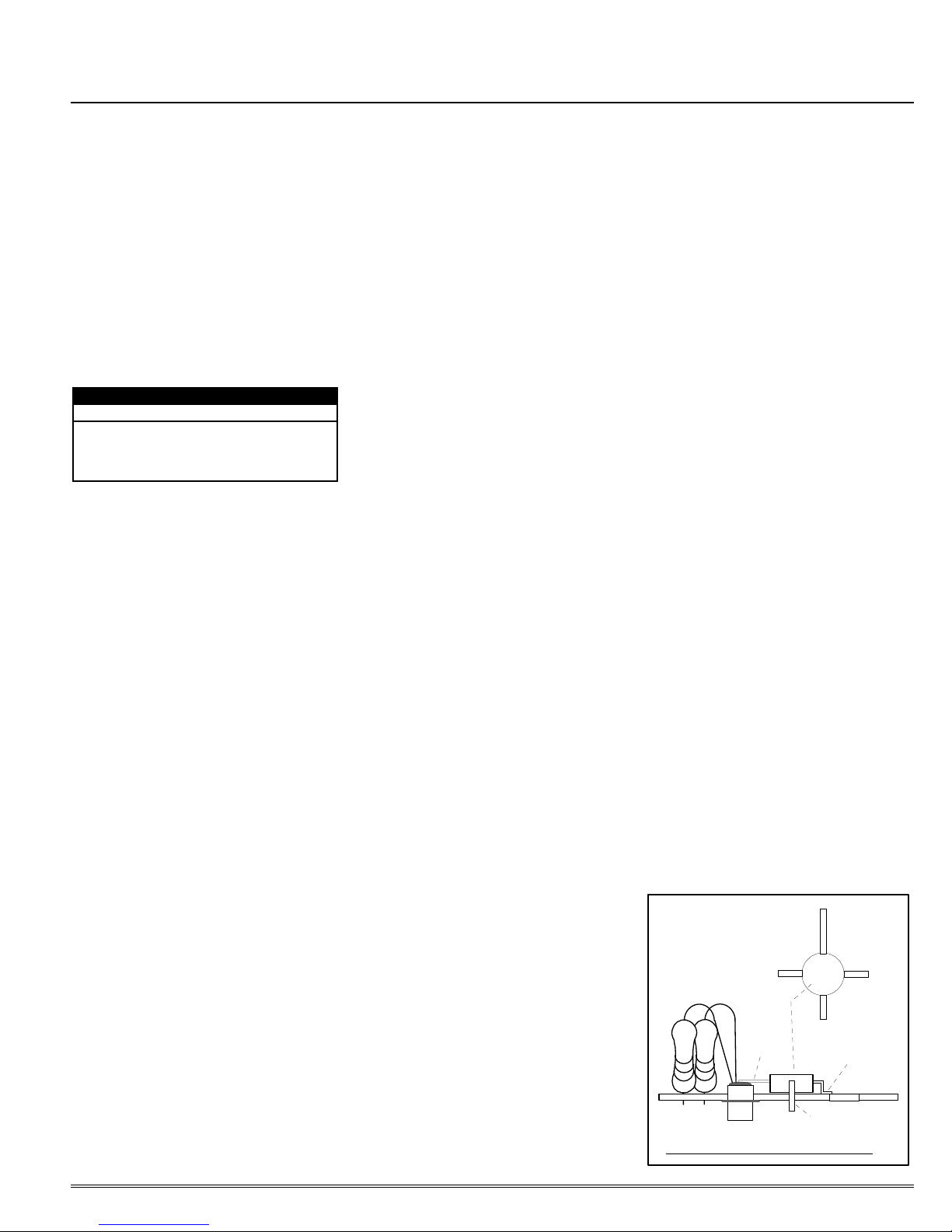
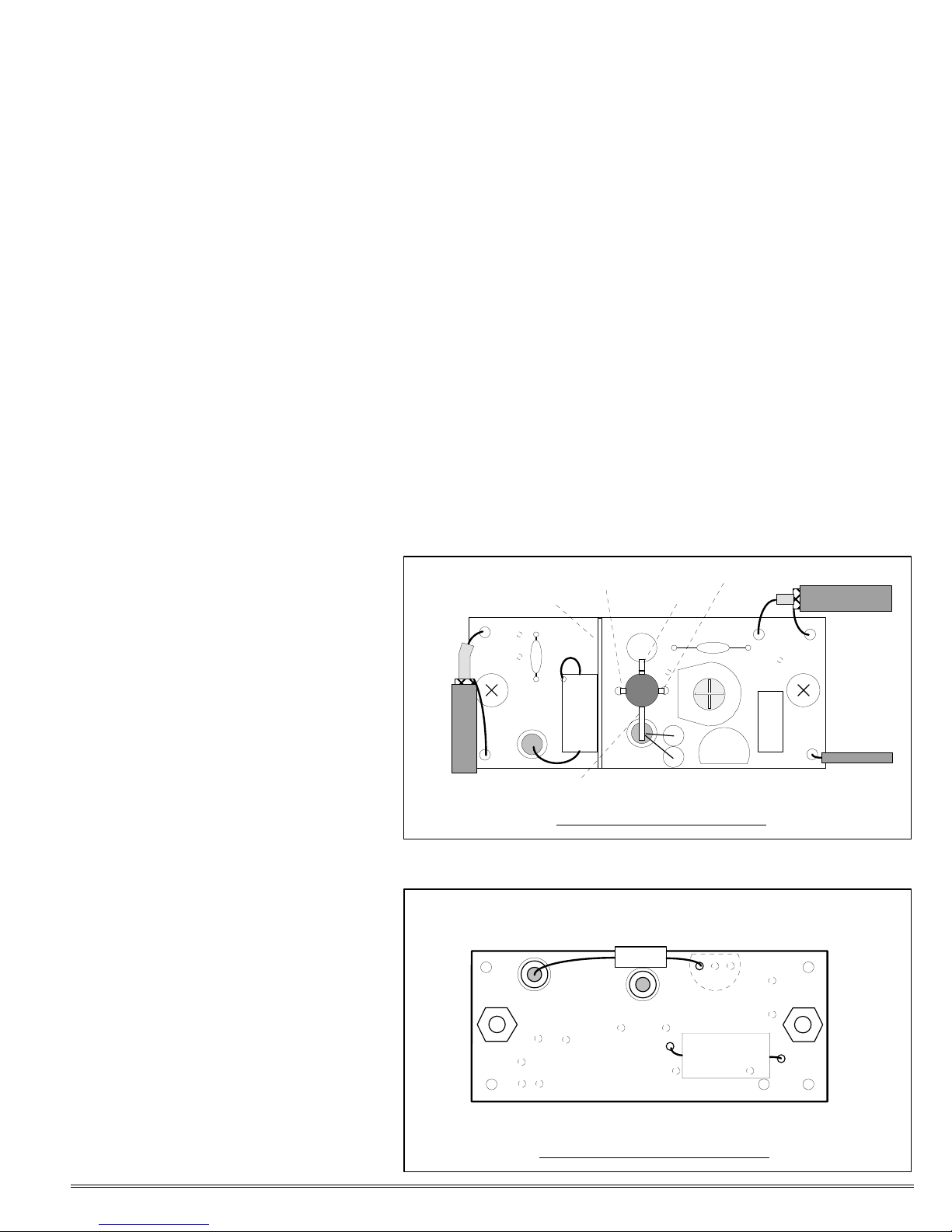
c. Figure 2 shows the placement of
Q1 on the board. The drain is the long
lead. Figure 1 shows how to form the
leads.
Pick up the transistor and orient it as
shown in figure 2 with lettering up.
Make sure you know which lead is
which. Gently bend the source, gate 1,
and drain leads down at a 90° angle as
shown in figure 1. Then, bend the bottom of the source lead out away from the
transistor to form an "L" shaped foot.
When formed properly, the transistor
will sit flush with the board as shown.
(The gate 2 lead is not bent.)
Insert the drain and gate 1 leads
through the holes in the board. The foot
formed in the source lead should rest on
the top of the board as shown in figures
1 and 2. Tack solder the foot of the
source lead to the board. Check that the
transistor is down against the board as
shown in figure 1. Check again that the
transistor is oriented properly with the
lettering up and the long lead in the hole
for the drain. Then, solder the gate 1
and drain leads to their pads under the
board. Trim off end of drain lead below
board.
Note: The feedthrough capacitors
have a hollow center which is metalized
through from end to end. Therefore, in
order to make a connection to the feedthru capacitor, simply insert a short
length of the lead into the hollow center
of the feedthru and solder to the metalization. It is not necessary for the lead to
go all the way to the other end because
there is metalization to conduct from one
end to the other.
Also note that the feedthru capacitor
by the transistor is not used as a feedthru
cap in the normal sense; it is merely used
as a very good vhf/uhf bypass capacitor
and tie point.
d. Install vertical resistors R1 and
R2 in the holes shown in figure 2. Solder their bottom leads. Then, refer to
figure 1 and bend the top leads over, inserting them into the center of ft capacitor C5. Trim these leads off at the
bottom. Bend the fet gate 2 lead over to
touch the top of the ft capacitor, and then
solder all three leads to the metalization
in the center of the capacitor. It is not
necessary to completely fill the capacitor
with solder as long as the three leads are
all soldered at the top.
e. Solder metal shield to ground
plane on top of pc board in position
shown in figure 2. Keep the shield as
close as possible to the transistor to leave
room for output coil L2. First, tack solder the shield to the board at each end.
DRAIN
IS LONG
LEAD
819
819
819819
ϖαλκ
ϖαλκ
ϖαλκϖαλκ
GATE 2
LETTERING
MUST BE UP
GATE 2
Figure 1. Transistor Lead Formation
SOURCE
GATE 1
SOURCE
GATE 1
©1995 Hamtronics, Inc.; Hilton NY; USA. All rights reserved. Hamtronics is a registered trademark. Revised: 12/14/02 - Page 1 -
Page 2
Once the shield is aligned properly, run
a bead of solder the whole length of the
shield. Then, run a second bead of solder on the other side of the shield. Soldering on both sides of the shield
provides maximum mechanical support
for the shield.
f. Install output coil L2 in the position shown. Form the lead to be soldered to the pc board so the coil fits
within the edges of the board. Insert the
other lead in the center of ft cap C8.
Solder both leads of L2.
g. Install C1, C2, and C3, keeping
leads short as possible. C2 should have
the rounded end to ground.
h. Install C7 and U1 in the holes
shown. The leads of C7 must be formed
to the narrower spacing of the pads on
the board.
i. Turn the preamp over, and orient
it as shown in figure 3. Position ferrite
bead Z1 as shown. Note that positioning
the body of the bead against the feedthrough capacitor prevents its leads from
shorting to anything. Solder one lead to
the inside metalization of ft cap C8, and
tack solder the other lead to the pad for
the left-hand lead of U1 as shown. If
there already is solder on the bottom of
C8, melt it and slide the lead in.
j. Install input coil L1 in the holes
shown. Form the leads so the coil fits
the holes and the coil rests about 1/16
inch away from the board.
Be sure that the coil leads are installed in the correct holes: the one on
the left should connect to the junction of
C1, C2, and gate 1 of the transistor; the
one on the right should connect to the
ground plane. Then, solder both leads.
After soldering on the bottom of the
board, trim the excess leads off on the
top of the board.
k. This completes construction.
Look over all components and solder
connections. Check for shorts or parts
in the wrong places.
INSTALLATION.
The preamp can be mounted to any
flat surface. Simply drill two 1/8 inch
holes 1-7/16 inch apart, and attach the
preamp with 4-40 screws and standoffs
or spacers as desired.
Complete shielding of the preamp is
not required. However, some care
should be given to selection of the
mounting location with regard to feedback from adjacent receiver circuits or rf
pickup if mounted very close to a transmitter circuit. Because the unit is small,
make sure that it isn't installed tight
against the rf amplifier or first mixer of
the receiver to minimize feedback effects.
Connect the input and output terminals in the receive signal path with
miniature coax, such as RG-174/u, as
shown in figure 2. Be sure to keep the
stripped pigtails as short as possible to
maintain a 50Ω path. Connections are
made by inserting the stripped ends of
the pigtails into the pads on the board
and soldering. Normally, the preamp is
mounted in some sort of enclosure with
UHF or similar connectors on the enclosure and miniature coax installed between the preamp and the large coax
connectors. In some cases, the output of
the preamp can go directly to the receiver with the miniature coax.
/ Caution: Don't connect the pre-
amp in the transmit signal path.
Connect power supply lead to E5.
The LNW requires filtered +10 to 15
Vdc. Current drain is about 10 mA.
LONG DRAIN LEAD
SHIELD
RF OUTPUT
COAX
E2
E1
C8
C3
L2
Q1
GATE 2
Figure 2. Top View of LNW Board
Caution is advised in selecting a
power source. Solid state amplifiers can
C8
Figure 3. Bottom View of LNW Board
be damaged by large voltage transients
and reverse polarity. Although protection is provided in the LNW in the form
of a voltage regulator ic, avoid such conditions as a matter of principle. Care
should be taken especially to install
a reverse diode across any inductive devices, such as relays, on the same B+
line to absorb transients.
ALIGNMENT.
Factory assembled preamps are tuned
at the center of the band. The bandwidth
is wide enough so that retuning normally
is not necessary because of frequency.
However, you may want to retune the
input circuitry to optimize noise figure
with the unit connected to your antenna.
Simply retune the input variable capacitor for best reception of weak signals.
No test equipment is necessary. If you
happen to have access to a signal generator and sinadder, they may be used; otherwise, just do it by ear.
TROUBLESHOOTING.
Since the unit is fairly simple, troubleshooting usually is limited to checking
GATE 1
SOURCE
RF INPUT
COAX
POWER
C5
C1
C2
R2
R1
U1
E3
E4
C7
E5
the dc voltages on the transistor. These
will vary somewhat; however, in gen-
Z1
C5
U1
L1
©1995 Hamtronics, Inc.; Hilton NY; USA. All rights reserved. Hamtronics is a registered trademark. Revised: 12/14/02 - Page 2 -
Page 3
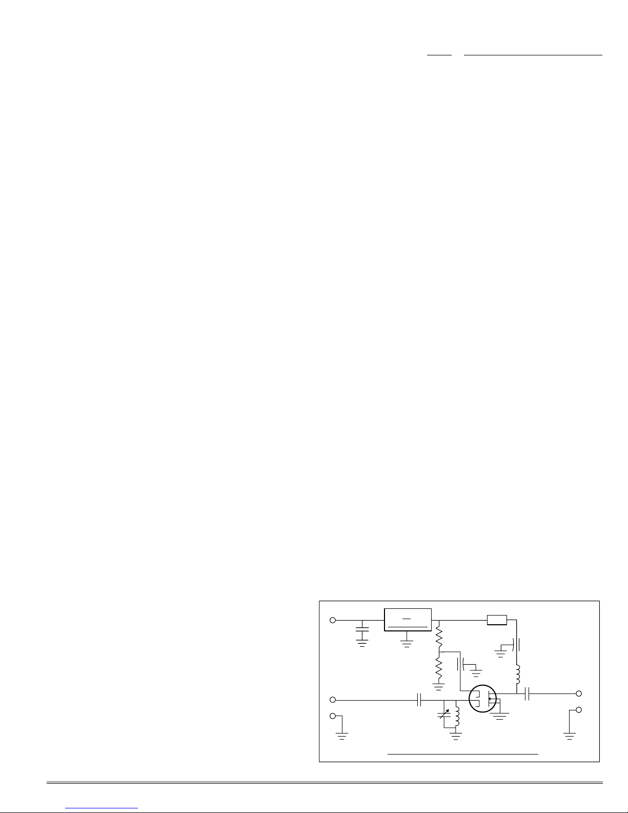
eral, the gate-2 voltage should be about 4
Vdc, and the drain should be at about 8
Vdc. The source and gate 1 should be at
ground potential.
If the dc voltages are OK but the unit
is no longer amplifying, assuming there
are no problems in the coax cabling, the
transistor may have been damaged by
transmitter rf or lightning discharge at
the antenna. Such damage often does
not cause a change in the dc characteristics of the transistor.
If the drain voltage is much lower
than 8 Vdc, first disconnect ferrite bead
Z1 to see if the transistor is shorting the
output of the voltage regulator. In the
case of a severe voltage transient or reverse B+ voltage, it is possible to also
damage the voltage regulator.
If the unit is amplifying OK but you
are experiencing intermod, you may be
overloading your receiver by adding gain
ahead of the rf stage. Low noise preamps are effective in improving sensitivity of receiver systems in weak signal
areas. However, it is normally considered inadvisable to use a preamp, even
with a well designed receiver, in very
strong signal areas, such as the center of
a city or other locations with high powered transmitters in the area.
Adding gain ahead of a receiver degrades the selectivity of a receiver by an
equivalent amount by boosting undesirable signals as well as desirable ones. In
severe cases, strong signals which do not
cause intermod by themselves will create
intermod in the rf stage or mixer of your
receiver after being amplified an additional 20 dB.
If you use a preamp with a repeater
receiver, you will need to have additional rejection in your duplexer to attenuate your transmit signal that much
more to prevent desense.
static sensitive; so be careful. It is
good to discharge your hand to a
grounded metal object just before picking
up the transistor, and the use of a
grounded soldering iron is mandatory.
A heat sink is not necessary while soldering, but be careful not to apply any more
heat than necessary.
You should not be overly anxious
about blowing out the transistor if you
observe the precautions above. The
transistors are all factory tested and
wrapped in foil to ensure that they arrive
in good condition. There is no warranty
coverage for damage which occurs in
handling.
Refer to ASSEMBLY section of
manual for details of how to install a
transistor.
REMOVING OTHER PARTS.
Because the pc board uses plated
through holes, all of the solder within the
holes must be removed before a lead can
be removed from the board. This can be
done with solder-wick or a vacuum
desoldering tool, as long as you remove
all the solder within the holes.
PARTS LIST.
Ref # Description
C1 10 pf disc (LNW-28 & LNW-50)
6 pf disc (LNW-75 & LNW-100)
C2 50 pf cer. variable (28 & 50)
20 pf cer. variable (LNW-75)
10 pf cer. variable (LNW-100)
C3 .001 µf disc (1nK or 1nM)
C4 not used
C5 .001µf feedthrough capacitor
C6 not used
C7 0.15µf mylar capacitor
C8 .001µf feedthrough capacitor
L1-L2 3µH coil [exposed wires]
(LNW-28)
0.33µH coil [orn-orn-sil-red]
(LNW-50)
0.22µH coil [red-red-sil-red]
(LNW-75 & LNW-100)
Q1 N.E.C. 3SK122 mosfet
R1-R2 100K
U1 78L08 Voltage Regulator IC
Z1 Ferrite Bead
TRANSISTOR
REPLACEMENT.
Transistor replacement is complicated
a little by the fact that the pc board has
plated-through holes. You must remove
all the solder from the drain and gate-1
leads before trying to pull the transistor
off the board. This can be done with
solder-wick or a vacuum desoldering
tool, as long as you remove all the solder
within the holes. Then, melt the solder
on the top of ft cap C5, and lift the gate2 lead of the transistor.
/ CAUTION: The small geometry
and high impedances make fet's heat and
©1995 Hamtronics, Inc.; Hilton NY; USA. All rights reserved. Hamtronics is a registered trademark. Revised: 12/14/02 - Page 3 -
E5
B+
(10-15V)
RF
INPUT
E3
E4
C7
U1
8-VOLT REG.
R1
R2
C1
C2
L1
Figure 4. LNW Preamp, Schematic Diagram
Z1
C8
C5
L2
Q1
C3
RF
OUTPUT
E2
E1
 Loading...