


ISSUE
4-
OCTOBER
1952
,

GENERAL PURPOSE
COMMUNICATIONS
MODEL
MODEL
INSTRUCTIONS
The
Model SP-600-J Receiver does
Frequency
Book
Receiver, all indications
and
diagrams,
trol
Unit,
With
Control
is used in connection
with
shouldbeignored as
this exception
SP-600-JX
AND
SP-600-J
MODEL
SP-600-J
Unit.
referencetothe
the
When
with
the
in
the
theydonot
two
models are identical.
this Instruction
Model SP-600-J
text,
Frequency
RECEIVER
not
have
photographs
Con.
apply.
the
460
West
THE
34th
ISSUE
Manufactured
4
by
HAMMARLUND MFG. CO. INC.
St.
Prinl~d
New York
inU.S.
A.
1,
New York,
U.S.A.

FRONT
Sp-
F\G.
VIEW
eOO-JX
OF
IN
CA81N
RECEIVER
ET

TABLE
OF
CONTENTS
Title
Technical
I
II
III
IV
V
VI
VII
Table
Table
Table
Table
Table
Summary
General
Circuit
Installation 7
Operation
Maintenance
Alignment.
ConversionofTable
I-Tube
2-Tube
3-RF
4-Approx.
5-Parts
Description 5
Description 6
. . . . . . . . . . . . . . . . . . . . . . . . . . . . . . . . . . . . . . . . . . . . . . . . . . . . . . . . . . . . . . . . . . . . . . . . . . . . . 16
Model
Socket
Socket
and
List
HF
Signal
Voltages..
Terminal
Oscillator
InputsatIF
Receiver for
.
..
Resistances.........
Alignment
and
Rack
Mounting
..
.
..
.
Frequencies ; . . . .
AF
Stages. . . . . . . . . . . . . . . . . . . . . . . . . . . . . . . . . . . . . . . . . . . . . . . 17
Page
, 20
..
4
8
10
14
15
17
21
Figure
Figure 2
Figure
Figure
Figure 5
Figure
Figure
Figure
Figure 9
Figure 10
Figure
11
Figure
12
Figure
13
Figure 14
ILLUSTRATIONS
Front
ViewofReceiver SP-600'
Block Diagram 7
Location
3
Audio
4
Selectivity
Rear
6
Top
7
Top
8
Bottom
Bottom
Bottom
Bottom
Circuit
Connection
of
Tubes
and
Overall Fidelity
Curves
ViewofReceiver. . . . . . . . . . . . . . . . . . . . . . . . . . . .... . . . . . . . . . . . . . .... . . . . . . . . . . . . .
ViewofReceiver. . . . . . . . . . . . . . . . . . . . . . . . . . . . . . . . . . . . . . . . . . . . . . . . . . . . . . . . . . . . . . . . 26
ViewofReceiver-Capacitor
ViewofReceiver-Tuning
ViewofReceiver
ViewofRF
ViewofFrequency
DiagramofReceiver. . . . . . . . . . . . . . . . . . . . . . . . . . . . . . . . . . . . . . . . . . . . . . . . . . . . . . . . .
Diagram-Receiver
and
Adjustments
Tube
]X,incabinet.
Curves.
SP·600·]X,
Platform.
Control
. . . . . . . . . . . . . . . . . . . . . . . . . . . . . . . . . . . . . . . . . . . . . . . . . .
Shield and Spare Fuse
Unit
. . . . . . . . . . .... . . . . . . . . . . . . . . .... . .... . . . . . . . . . . . .
. . . . . . . . . . . . . . . . . . . . . . . . . . . . . . . . . . . . . . . . . . . . . . . . . .
Unit.
Chassis. . . . . . . . . . . . . . . . . . . . . . . . . . . . . . . . . . . . . . . . . . . . . . .
. . . . . . . . . . . . . . . . . . . . . . . . . . . . . . . . . . . . . . . . . . . 2
'.
. . . . . . . . . . . . . . . . . . . . . . . . . . . .
Cover
Removed.
Shield
Removed.
. . . . . . . . . . . . . . . . . . . . . . . . . . . . . . . . . . . . . . . . . . . . .
. . . . . . . . . . . . . . . . . . . . . . . . . . . . . . . . . 28
. . . . . . . . . . . . . . . . .
..
18
..
18
19
..
25
..
27
..
29
..
30
..
31
..
33
..
35
Figure
Figure
Connection
15
Connection
16
Diagram-Tuning
Diagram-Frequency
Unit.
Control
Unit..........................................
[ 3 ]
, " .
37
39

GENERAL PURPOSE
MODEL SP-600-JX
COMMUNICATIONS
RECEIVER
TECHNICAL
SUMMARY
Electrical Characteristics
Frequency
Power
Output
Range-total
Band
1 .
Band
2 .
Band
3 : .
Band4.........................•..........••.................................
Band
5 .
Band
6 : .
Output-2.0
Impedance-6OO
Phone
600
jack-winding;
ohm
power
6
bands
watts,
with
less
than10percent
ohms-balanced split windings.
delivers15milliwattstoan
load is
adjustedto500 milliwatts.
distortion.
8000
ohm
resistive load,
when
the
Power Supply Requirements
Lil"
.~lting...........................
Power
Tube
RF,IFand
HF,
Crystal
Mixers
Detector,
AF
Power
Rectifier 1Voltage
Consumption.
. . . . . . . . . . . . . . . . . . . . . . . . . . . . . . .
Complement-total
BFO
Amplifiers 7 -
2nd
Conversion
Controlled
and
HF
BFO
Oscillator.
"c" Bias Rectifier
Amplifier
Output
andIFOutput.
Regulator.
. . . . . . . . . . . . . . . . . . . . . . . . . . . . . . . . . . . . . . . . . . . . . . . . . . . . . . . . . . . . . . . ...1 -
20
Oscillators 3 - 6C4
. . . . . . . . . . . . . . . . . . . . . . . . . . . . . . . . . . . . . . . . . . . . . . . . . . ...1 -
and
Noise
. . . . . . . . . . . . . . . . . . . . . . . . . . . . . . . . . . . . . . . . . . . . . . . . . . . . . ...1-
95, 105, 117, DO,
Limiter&'Meter
190,210,234
..
130
watts,
Rectifier 3 - 6AL5
and
260 volt taps, 50·60 cycles.
1.25 amps.at117
.
.54to54.0
.54to1.35 me
to
1.35
to
3.45
to
7.40
to
14.80
to
29.70
audio
output
volts--maximum.
2 - 6BE6
1-
mc
3.45 mc
7.40 mc
14.8 me
29.7 me
54.0 mc
to
the
6BA6
6AC7
12AU7
6V6GT
5R4GY
OA2
Mechanical Specifications
Rack
Modelsurface.
Table
Weight
Model-Dimensions;
Performance
Sensitivity is 2.3 microvolts,
10
db,at20
Image
rejection ratios are
TheIFrejection ratio at 600 kc is 2700 to
TheAVC
200,000 microvolts.
Dimensions; 19
66 lbs.
21%
Data-
milliwatts
action will maintain
(approximate
or
output
better
inches
inches wide,
better,
and
with
than
the
wide,
IOYz
inches
12~
values-takenona sample receiver)
throughout
the
RF
74
db
1.
output
the
Gain
throughout
constant
high
inches
high
entire
frequency
Control
at maximum.
the
frequency
within12db
and
16]/z inches deep from rack mounting
and
when
[ 4 )
171'8 inches deep.
range, for a signaltonoise ratio
range.
the
input
Weight
is increased from 2
87]/z Ibs.
of
to

GENERAL PURPOSE
COMMUNICATIONS
GENERAL DESCRIPTION
The
SP-600-]X is a20tube
with
self
Receiver
suffix in
is made using
are
insofar
steel, table model cabinet finished in dark grey
complement
ingina
operation
ing
primaryisprovided
range
is 130 watts.
loudspeaker receptionofAM
telegraph,
diversity applications.
over
in six bands.
control knob,
frequency
a small
band
indicator
hasanarbitrary
vernier
each frequency
and
design
exceptional
and
extremely close calibration accuracy
accurate resetability. A
locking action
main dial is 50to1
to
provided on all bands. Single conversion is used
signal frequenciesupto
employing a crystal controlled oscillator,
frequencies above 7.4 me.
tion,
meter
the
model
the
equivalentofmilitary
as is practicable.
The
receiver is suppliedineither
the
standard19inch
The
self
contained
from
current
The
The
a frequency
in use.
In
additiontothe
resetability.
The
vernier
The
the
Two
power
from90to
receiver is suitable
AM
standard
band
front
This
with
dial provides
single
to
permit
operating
dials.
tuning
main dial is 6to1.
stages
detector
rectifier,
contained
number
components
lighter
a single phase, 50to60 cycle alternat-
The
on
panel
the
tuning
without
ratio
of
andAVC
beat
grey
power
source.
with
270
volts.
MCW
model provides continuous coverage
range
large easily operated
the
front
andaband
window
control also aligns
proper
frequency
scale
whichinconjunction
continuous
band
for
control
maximum
ease.Itcontrols
An
anti-backlash gear
affecting
from
and
radio
frequency
Radio Communications
power
denotes
having
component
front
relay rack.
supply is designed
The
taps covering a line voltage
The
for
telegraph
from 0.54to54.0 megacycles
panel, selects
indicator
indicates
dial scale.
extremely accurate logging
is large
traverse
tuning
the
the
ratio
frequency
7.4 mc
and
Four
rectifier, noise limiter
supply.
that
characteristics
a well ventilated
panelorfor
power
power
either
headphone
radio telephone,
signals
visible
the
the
dial frequency
scales,
expanded
andofspecial
speed as well as
both
and
lock provides positive
the
frequency setting.
tuning
controltothe
from
the
amplification are
double conversion,
stagesofIF
oscillator
The
this
receiver
which
specifications
meunt-
transformer
consumption
and
band
change
the
desired
through
frequency
the
main dial
with
scales
the
train
provides
completely
vernier dial
for
amplifica-
and
buffer
to
fo~
or
CW
for
the
over
main
for
signal
and
I
amplifier,IFoutput,
]
stage are provided.
The
frequency control
channel
quencies
panel controls
stability continuously variable
six selected fixed frequency signals.
trolled fixed channel
set
crystal frequency desired
frequency control.
with
order
the
ference from ignition systemsorother
type
of
a balanced line.
95 ohms.
conventional single wire antenna.
loadorline
winding
output
circuit
signals
ohm
but
tion
ments
installations.
ranges between .001
quency depending on
very unusual degree of frequency stability
tuned
stability.
crystal
ranging
crystal filter embodies
have
Super
mechanical design.
crystal controlled operation
within
the
dial to
the
from
signal frequency
The
noise limiter circuit effectively limits
noise.
the
limiter.
The
antenna
The
audio
for
is approximately 2.0 watts.
when
attenuated
power
The
send receive switch desensitizes
leaves
between transmission periods.
Radiation is negligible
for
Frequency
HF
The
selectivity control provides
and
from
provedsoeffective
Pro
the
range from .75to54 mc.
permit
operationitis
the
signal frequency, switchtothe
These
receiver,
HAMMARLUND
The
output.
the
shipboard operation
oscillators
but
for
The
limiter switch permits optional use
input
The
receiver may alsobeoperated
output
and
balanced load operation.
three
Receivers, incorporated in an improved
circuit is designed
is provided
referredtoan 8000
approximately15db
poweronto
drift
aftera15
degrees
sharp
(.2 kc)tobroad
RECEIVER
AF
amplifier
the
selectionofthe
and
crystals are
may be purchased
which
circuit is designed
input
provide
and
percent
the
frequency used.
and
closely approaches crystal
of
the
same circuit features
and
and
output
unit
provides
on
tuningoreitherofthe
For
only
tune
with
MFG.
CO.
each istofunction.
sourcesofpulse
impedance is nominally
for
withafour
Maximum
The
ohm
below
for
complies
and
for
minute
desirable in
warmupperiod,
and
.01
percentoffre-
three
non-crystal selectivity
(13.0
power
for
fixed
any
six fre-
Front
normal
necessary to
not
for
terminal split
load provides
the
instant
with
multi-receiver
Hammarlund
high
crystal con-
the
delta
supplied
on
special
specifying
the
inter-
use
with
with
a 600
ohm
power
headphone
the
600
receiver
recep-
require-
This
is a
for
variable
degrees
kc).
The
that
of
a
[ 5 ]

CIRCUIT DESCRIPTION
GeneralFigure 13. A block diagram, Figure 2, is provided
more
clearly
the
various circuit sections.
tubesisshowninFigure
conversion, used
consists
V-2, First
four
stagesofIF
Vll,
Detector
V-IS,
AF
amplifier
V-17
and
Power
B
Voltage
In
the
frequencies above 7.4 me,
Second
the
Gate
Input
to
provide
mission line. A
antenna
RF
turretisemployedtochange
coil assembliesoftheRFamplifier
V-5
and
rectly
gang
tuning
assures maximum sensitivityathigh
ratio.
First
The
rotary
signofthe
capacitor
vide
frequency
to
a previously
First
V-3)-For
frequency
quency
variable
of
six crystal positions, is effectedbya
control. A second
mentofthe
or
minus .005
Intermediate
sionto455 kc is employed
7.4 me.
incorporating
circuit. Six positions
widthsof.2, .5, 1.3, 3, 8,
narrower
operation.
treme selectivity
adjacent
The
circuit is
show
the
for
signal frequencies
of
two
stagesofRF
Mixer
V-5,
First
amplification V-7, V-9, YolO
and
AVe
Beat
Frequency
V-16-A
the
Rectifier
Regulator
circuit
Heterodyne
tube
Coupling-The
optimum
maybeused.
Amplifier -
First
adjacenttotheir
capacitor
Heterodyne
turret
four
and
Heterodyne
services
operation, a crystal controlled
oscillator is provided.
to
crystal controlled oscillator
crystal oscillator frequency
There
bandwidth
The
interfering
and
Power
V-19,
V-18.
for
double
Oscillator
V-7.
coupling from a
balanced
An
Heterodyne
and
Oscillator-
band
gang,
rugged
stability
unattained
Oscillator-
requiring
front
percent
Frequency
are
four
the
Hammarlund
of
positions,
crystal
for
the
signals.
shown
arrangement
The
3.
Heterodyne
rectifier V-14, Noise Limiter
Oscillator
V-16-B,
Supply
C Bias Rectifier V-20
conversion, used
the
antenna
doublet
ingeniously designed
bands
Oscillator
respective sectionsofthe
their
change
twin
section, variable
construction
and
dial calibration accuracy
degree.
Instant
panel control permits adjust-
range.
Amplifier - Single conver-
for
signal frequencies below
stages
selectivity provide 6dbband-
and
phasing
high
schematically in
and
functions
locationofthe
The
circuit,
amplification
Oscillator V-4,
V-l3,IFoutput
Output
system
Second
V-8
which
Mixer
are
substituted
coupling is designed
95
or
andtoplace
V-I
and
V-4
respective tubes.
signaltonoise
(Variable
switch, advanced de-
throughout,
(Crystal
extremely stable, fixed
changeover from
of
IF
patented
13
kc.
the
crystal filter is in
control provides ex-
attenuation
various
for
single
upto7.4 me
V-I
Power
stage
includes
for
signal
V-6
ohm
trans-
straight
rotary
V-2,
Mixer
stages di-
V-4)-
tuning
Controlled
high
with
a choice
front
panel
over
a plus
amplification
crystal filter
On
the
of
closely
to
of
and
and
and
and
and
for
wire
the
four
This
pro-
fre-
three
II
for
Double conversion is employed
cies above 7.4 me.
by
the
me
V-4orV-3
signal is
Mixer
Oscillator
Detector
high level
circuit is provided
for
output
applications.
Beat Frequency Oscillator oscillator employs a
which
minimizes oscillator harmonics.
Oscillator
through
lator lock-in
injection
the
beat
Noise Limiter -
limits
other
switch
modeofoperation
present.
Audio
amplifier triode
signal from
Audio
transformer
to
deliver 2.0
load.
of
the
teletypeorsimilar service. A separate secondary winding provides attenuated audio signal
phone
of15milliwatts into an 8000
the
wattstoa 600
IF
a 70
(455 kc)
chassis. A PL-259 plug
plied,
Power
partofthe
and
low pass filters
power
primary taps, covering a power line source range
90to270 volts, 50to60 cycles.
former
the
in
First
then
V-6
and
V-8,
andAVC-The
Detector
CW
and
terminals provide
gives a
von,
Buffer Amplifier V-12,
by
chassis. A
frequency, from zero
the
noise interference from ignition systems
sourcesofpulse
5-6, permits optional useofthe
Frequency Amplifier - A resistance coupled
Output-The
The
split balanced winding permits balancing
direct
operation.
600
ohm
Output
ohm
impedance source of intermediate frequency
to
are
used
Supply-The
the
e rectifierV-20,
transformerisprovided
and
primary
The
signalisheterodynedto3.955
Mixer
V-5
and
for
high
image rejection.
heterodynedto455 kcbythe
the
3.5 me Fixed
for
selectivity.
V-14
and
Ave
with
separate time constants
MCW
high
and
meansofa control locatedonthe
front
V-16-B, amplifies
the
detector.
coupled
watts un
currentinthe
power
ohm
- A cathode follower
socket,
for
receiver.Itincludes
and
filter components are protectedbyfuses
and
operation.
for
connections in diversity
high
capacity Colpitts circuit
orderoffrequency stability
is coupled into
which
permits variationofthe
Panel
control
beattoplusorminus 3 kc.
The
noise limiter circuit
type
noise. A separate control
when
pulse
audio
through
This
secondary is delivering 500 milli-
resistive load.
SO-
this
the
plate supply circuits.
a split, balanced
distorted
output
winding will deliver an
ohm
239,onthe
and
RG-ll/U
connection.
power
together
Voltage
signal frequen-
Heterodyne
The
Crystal
tube
is used as a
Rectifier.
Ave
The
beat
The
beat
the
detector
eliminates oscil-
beat
varies
limiteronany
type
interference is
the
audio frequency
output
outputtoa 600
supplyisan integral
Regulator
tube
circuit, as used
output
resistive load
V-16-A
rear
skirtofthe
cable,
the
B rectifier V -19
with
their
with
screw terminal
The
power trans-
Oscillator
3.955 me
Second
Controlled
TheAVC
and
Diode
frequency
and
frequency
circuit
oscillator
rear
the
audio
V-IS,
V-17, is
winding
ohm
for
for
head-
output
when
provides
not
sup-
respective
V-18.
The
of
or
of
[ 6 ]

Tuning
Meter-The
operationtoindicate
relative
the
tionofoutput
control is
to
erating
"MANUAL"
when
Power
clockwise
strengthofreceived signals. Depression
Meter
Switch
converts
level indbfrom 6 milliwatts.
RF
Gain
Control
provided
prevent
overloading
with
the
position.
the
switch is in
"ON-OFF"
extremityofthe
tuning
the
and
Power
for
AYC-MANUAL
switch is
meter is usedonA
accuracyoftuning
the
meter circuit
Switch -
The
manual controlofsensitivity
on
strong signals
switch in
This
control also operates
the"AYC"
position.
operatedatthe
RF
gain control.
3.5mc
CRYSTAL CONTROLLED
and
for
indica-
RF
when
counter-
YC
the
of
gain
opthe
The
Send-Receive
sensitizes
provide
for
the
receiver
instant
Switch-The
but
leaves
reception
send-receive switch de-
the
power
between
"on"
transmission
periods.
Convenience
is provided
tionofan accessory
Radiation high
frequency, second conversion crystal
frequency oscillators
negligible
on
point
Outlet
- A convenience power outlet
the
rearofthe
such
Advanced
so
that
chassis
for
the
as a lamporelectric clock.
design
has
and
shieldingofthe
reduced radiation
interferenceofthis
connec-
and
nature,
commoninmulti-receiver installations, is reduced
a minimum.
beat
to
to
a
to
VI
RF
6BA6
•BLOCK DIAGRAM'
Tubes
and
Packing-After
that
all
see
any
packing
Power
leadatthe
nectedtothe
tubes
material is removed from
Supply-Make
bottomofthe
tap
50to60 cycle
Antenna-The
socket,
UG-103/U,
transmission line.
and
connector
ceiver, are
be
used
desired
antenna
terminal
should
plug,
for
with
a balanced
to
operate
lead-in wire should
of
the
be
connected from
V2
RF
6BA6
V3
FFO
6Ar;r
CRYSTAL CONTROLLED
unpacking
are
firmly in
sure
their
that
power
which
most nearly agrees
power
source voltage.
input
impedanceatthe
is designedtomatch a 95
The
angle plug adapter,
use
UG-102/U,
with
RG-22/U
supplied
antenna
with
a single wire
be
connector
plug
the
other
andaground
FIG.
INSTALLATION
the
receiver
sockets
the
transformer
cable
installation.Ifit is
connected
and
that
the
receiver.
primary
tap
is con-
with
the
antenna
ohm
UG-I04/U,
with
the
re-
which
should
antenna,
to
the
one
lead
terminalofthe
IF
OUTPUT
2
III
connector plug
to
peak
the
of
the
to
to
of
the
adjacent
ing
unit.
Speaker-The
magnet dynamic
voice coil
connectiontothe
the
receiver.
not
used, connect a 600
terminals
transient
insertion
voltages,
sections
the
insertion circuit, such as a low resistance balancing
potentiometer, connected
Headphones-Either
---
••••••••••••
-----
antenna
to
Signal
Signal
•
the
ground
socketatthe
speaker shouldbeof
type
and
600
ohm
line matching
600
ohm
Caution:
When
ohm,2watt
avoid
voltages.
direct
jumper
600
ohm
component
For
current
connecting
output
in
highorlow impedance head-
V16B
AFAMP
12AU7
V15A
LIMITER
6AL5
path
path
".
cammon 10
tor
V17
OUTPUT
6V6GT
V15B
METER
6AL5
TO
OUTPUT
LEVEL
METER
01/
frequencies above 7.4 mc
terminal,
frequencies
• below 7.4 me
which
rearofthe
the
permanent
tun-
should include a speaker
audio
the
transformer
output
600
ohm
terminals
for
of
output
resistortothese
damage from
applications requiring
control
the
or
two
high
the
indicating
balanced
may be reMoved and
its place.
is
is
[ 7 ]
phones
jack, locatedatthe
The
table
in
protective·
bottom
standard19inch
See Section
position
Y6, are
supplied
in
order
operation, crystal units may be ordered from
MARLUND
specify
be
loosen
quency
spring
crystalsinthe
retainer
press
thumb
each crystal
chart
maybeusedbyplug
high
impedance
Mounting-The
or
rack mounting.
a well
Crystals
the
used. See
ventilated
rubber
cover
plates are supplied
VII.
which
permits
for
Frequency
not
supplied
on
special
rangeofthe
to
insure correct crystal controlled frequency
MFG.
the
signal
noteatendofTable5.To
the
knurled
Control
assembly
sockets,
spring
on
screw.
provided
assembly
topofthe
Mark
was
selected, in megacyclesonthe
for
connectiontothe
lower
left sideofthe
type
is recommended.
receiver is designed
Table
models are supplied
steel cabinet
feet.
Rack
rack.
The
panel is
The
receiver should be placed in a
the
free accessofair.
Control
with
the
order
for
receiver above .75 megacycle.
CO.
INC.
frequency,
thumb
Unit,
to
this
screw
T34,
the
rear.
numbered1to6.Bring
forwardsothat
crystal
the
signal frequency
purpose
with
models,
for
lOYz
- Crystals, Y 1
receiver,
any
signal frequency
and
the
for
which
on
and
push
Insert
holders
alongside
handles
with
mountingina
inches high.
order
each
install crystals,
topofthe
the
the
and
front
but
the
tighten
for
the
phone
panel.
for
either
top
will be
HAM-
should
unitisto
retainer
crystal
springs
which
plastic
crystal
and
and
In
Fre-
or
the
the
to
switch, S2. Pencil
erased
time.
that
positions, which are also indicated
selector switch.
the
be
terminalsofthe
S9 is left in
A
load are provided
versity applications.
are
these terminals are
rearofthe
teletype
kc, intermediate frequency
and
an
resistive load,
microvolts signal.
at
an
ifitis
The
numeralsonthe
they
agree with
Relay Connections -
send-receive function is desired, connection may
madebysoldering a
the
VC
and
A
VC
provided
IF
Output-TheIFOutput
RG-lljU
outputofapproximately 200 millivoltstoa 70
Convenience
the
accessory, such asanelectric clockorlamp.
Diode
bus
and
chassis provides
or
other
rearofthe
or
ink may be used
desiredtochange
the
numeralsonthe
If
twin
Send-Receive switch, S9.
Sendoropen
Output-Shunt
series connectiontothe
at
the
rearofthe
The
with
a wire
not
used for external connection.
applications
is
cable should be used.
with
a normal sensitivity
Outlet-The
chassis may be used
these figures at
chart
external relay operation
conductor
position.
Diode
jumper
socket, SO-239, at
for
connection in diversity,
where
required. A PL-259 plug
power
and
should be used so
crystal socket
by
cabletothe
connection to
detector diode
receiver for di-
Output
connection
a sourceof455
This
will provide
input
outlet receptacle
for
can be
the
crystal
In
this case
terminals
operating
any
for
the
when
the
ohm
of
2
GeneralSP-600 receiver,
familiarize himself
various controls.
this
description,
the
partofthe
front
paneloron
example,
trol,
the
legend
to
photographs,
ing
this
are
shown
are
shown
Selectivity
is a 6-position switch
three
non-crystal degreesofselectivity, ranging from
extremely
fidelity
dial indicates
Phasing
control
It
permits
acteristic
channel
frequency.
RF
Before
When
the
name
when
referringtothe
word
SELECTIVITY
appearing
description.
in Fig.
sharp
mcw
is a differential
adjustmentofthe
for
interference
Gain
adjacenttothe
Figs. 1
in Fig. 1
6.
Control-The
for
operation.
the6db
Control-
high
Control-
attempting
the
operator
with
the
referringtothe
words
in capital letters represent
adjacenttothe
the
rear
and
6, is suggested while read-
Front
and
rear
which
cw receptiontobroad for good
The
bandwidthateach setting.
The
type,
attenuation
on
either
The
operation
should
functions
skirtofthe
in capitals indicates
panel controls
SELECTIVITY
selects
SELECTIVITY
CRYSTAL
crystal selectivity char-
RF
and
controlonthe
SELECTIVITY
control. Reference
controls
three
variable air capacitor.
of
closely adjacent
side
GAIN
IV
OPERATION
of
the
thoroughly
usesofthe
controls in
chassis.
and
crystal and
PHASING
of
control varies
For
con-
the
and
dials
terminals
control
control
the signal
the
overall gainofthe
either
tive in
Power
combined
counter-clockwise rotation
throws
catedonthe
Audio
varies
the
controlisalso operative in either positionofthe A
MAN
Phones
operating
jack
to
receive
isinthe
separate secondary winding
former, which provides an
phones. See Section
Audio
ableatthe
chassis for connection to a 600
III
installation.
Noise Limiter-
the
noise peak limiter inoroutofthe
control is operative independentlyofany
any
other
positionofthe
Switch -
with
the
power switch to
RF
Gain
Control-
input
switch.
Jack -
with
any
standard single circuit
circuitatall times
Output-The
four
control. See SectionIICircuit Description.
receiver.
The
power,
the
RF
GAIN
of
GAIN
voltage to
The
screw terminal
PHONES
the
sleeve
III
The
control dial.
The
the
of
attenuated
installation.
AUDIO
LIMITER
This
control is opera-
AVC-MAN
or
control. Complete
the
RF
the
off position,asindi-
AUDIO
audio amplifier.
jack is a single circuit
grounded
and
the
audio
OUTPUTisavail-
boardatthe
ohm
switch.
on-off switch is
GAIN
GAIN
andissuitable
phone
is connectedtoa
output
signal
rearofthe
load. See Section
control switches
circuit.
position
control
control
plug.
for
This
VC-
It
trans-
head-
This
of
[ 8 ]
A
VC-Manual
AVC-MAN
to
the
controlled
holding
wide
minimizes
received signal
when
strength
A
indication
received signals.
on
tionally
meter
below
A
and
by
in
lator
theAVC
keying.
lator
for
reception.
trol varies
oscillator
3 kilocycles.
cathode
fier,
detector
pole, single
tionitdesensitizes
and
rotates
and
quency
arbitrary
o
pointerofthe
plete
dial
scaleofthe
the
this
vernier
over
vernier
points. Since
on
into
mits
of
the
the
variation in
tuning
while traversing a
VC
position
AVC
operation,
strong
is less effective
maximum setting.
VC
potential is removed from
the
gainofthe
the
RF
CW-Modulation
the
CW
and
In
is inoperative
either
Beat
Frequency
over
BFO
Injection -
self biasofthe
thereby
tube.
Send-Receive -
3.5
me oscillator tubes
Tuning
the
vernier
band
outer
to
100 scale.
revolutions
at
any
vernier
setting is read, 487.6.
system divides
each
divisions,
the
vernier
approximately 6000 readable settings.
extreme
stations.
Tuning
rightofthe
Switch-In
switch applies
RF
audio
output
the
strengthofreceived signals.
the
variationofoutput
and
prevents
through
the
RF
of
tuning
GAIN
position energizes
connects an additional
circuittoaccommodate
the
voice modulatedortone
the
throw
Control
main
tuning
setting.
main dial indicates
dial indicates 87.6,
frequency
Lock -
resonance
The
when
signalsorto
control.
Switch-The
MOD
position
and
Oscillator -
tuningofthe
a range from zero
The
determining
The
toggle switch.Inthe
theRFamplifier, gate, second mixer
and
tuning
dials.
scales, calibrated in megacycles,
scale.
The
The
numeral
main dial indicates
that
Thus,ifthe
with
itiseasytoestimate
scale,
this
accuracyinthe
The
TUNING
automatic
andIFamplifier tubes, therel-y
relatively
blasting
signals
frequency
Meter
RF
GAIN
necessarytocontrol excep-
reduce
when
the
In
the
receiver is manually controlled
the
the
the
conditions are established
BFO
beat
frequency
the
injection voltagetothe
SEND-
during
Dials -
capacitor as well as
The
vernier
under
have
been
This
the
rotationofthe
band
into approximately 600
one-half division calibration
divides each frequency
TUNING
control, provides a positive
theAVC
duetofadingofthe
of
circuit is operative for
and
control is operative
RF
MAN
the
beat
timing
beat
The
455 kc
beattoplusorminus
IN]
REC
transmission periods.
The
main dial has six fre-
dial has an
the
madebythe
pointer
over
the
logging
pOSItIon
bIas
constant
and
overloading
greatly different
band.
relative
CW-MOD
theAVC
control adjusts
precise mechanical
one-tenth
LOCK,
strength
noise,
but
GAIN
position
controlled
frequency oscil-
capacitor
frequency
modulated signal
BEAT
beat
buffer ampli-
controlisa single
SEND
TUNING
the
upperorfixed
numberofcom-
for
the
figure 4
readingtolog for
and
the
potenti1',
over a
This
In
the
the
RF
control
the
tubes
control
to slow
oscil-
OSC
con-
frequency
the
posi-
control
the
main
and
arbitrary
vernier
the
outer
and
main dial
divisions
band
This
per-
resetting
located
of
to
an
to
lock
for
the
tuning
frequency setting
dental
shiftingofthe
Band
Change-Each
CHANGE
RF
and
assemblies, from one frequency
turret
tion desired. A positive
correct location
CHANGE
MEGACYCLES
centerofthe
is
cator
Crystal
control selects
operation
which
the
in
tion.
small frequency tolerancetowhich
made.
Meter
pole, double
to
theRFposition. See SectionIICircuit Description,
Tuning
Tuning
control is usedtoadjust
meter
RF
position.
plus 20dbon
microvolt
switch in
METER
circuit
db
from 6 milliwatts.
the
RF
pressed
been adjusted
headphonesorspeaker. Failuretoobserve
tion
may
AD]
when
adjusted
the
meter
from
justed
resistive load.
Preliminary to
"on"byturning
advance this control
lIght. Place
the
BAND
in
whichitis desiredtooperate.
at
least15minutes before using
to
permit
pluginthe
See Installation, Section III.
MCW
its extreme counter-clockwise position and
SELECTIVITY
control
HF
Oscillator coil,
hasnostops
control simultaneously operates
panel
with
the
Controlled
either
or
anyone
similarly numbered crystal sockets
Crystal
The
DELTA
Switch-The
throw
Meter.
Meter
when
the
It
RF
input
theAVC
switchtothe
for
indicationofthe
position
for
the
result in damagetothe
AF
control is usedtoregulate
operating
to
obtain a 0dbreading on
and
the
600
ohm
to
6 milliwatts,
the
CHANGE
the
tubestowarm
PHONES
Reception -
mechanism
whenitis desiredtoprevent
tuning.
turns
and
may be
of
the
various bands.
band
indicating dial, located at
and
aligns
proper
Control
scaleofthe
HF
variable
of
Unit.
FREQ
METER
toggle switch
Controls-
METER
is adjustedtoproduce a reading
the
RF
scaleofthe
signal
position. Depression
AF
This
when
released
AF
scale unless
for
low
power
on
the
is made
SEND-REC
switch to 3 kc.
with
AUDIO
or
Operation-Turn
the
RF
GAIN
to
10.
controltothe
jackoruse speaker as desired.
Turn
without
revolution
the
turret,
trimmer
bandtothe
turnedineither
detent
the
Oscillator -
high
the
six crystal positions,
See Section
control compensates
The
the
resistance
switch isinthe
and
with
position
AF
power
switch is
and
the
output,
meter.
AF
scale.
the
audio
OUTPUT
1.9 volts across a 600
control clockwise
Note
switchonREC
This
the
up.
Insert
the
TUNING
affecting
of
the
containing
and
switch contact
next.
mechanism assures
The
dial
frequency
main dial.
The
frequency
are
III
the
crystals
switch is a double
with
spring
METER
shunting
normal,
meter,
converts
should
the
the
that
receiver, in
Put
the
AVC-MAN
output
spring
notbede-
audio
output
by
this
The
meter
This
the
AF
power
terminals ad-
power
the
dial lamps
frequency
should be
the
headphones
the
CW-MOD
with
control is
LOCK
the
acci-
BAND
the
The
direc-
BAND
the
small
indi-
XT
ALS
oscillator
provided
Installa-
for
return
AD]
a
of
the
meter
level in
return
means
precau-
METER
current
scale
output
ohm
switch
and
and
turn
band
done
order
turn
the
for
the
are
RF
the
or
of
10
the
to
has
of
of
to
the
[ 9 ]

switchonMOD,
AVC-MAN
controlatits
switchtoVFO.
the
proper
in
as indicated
AUDIO
the
quencyonthe
mum responseorindication
.resonance
quarterofone
just
level
fully
wise,ifdesired.
turnedtothe
frequency
ciently high.
TIVITY
which
LIMITER
SELECTIVITY
positions,
justedtoeither
an
may be
stand-by
the
The
GAIN
AVC-MAN
very
throwntoCW
Locate
then
fixed
which
Installation.
correspondingtothatonthe
GAIN
TUNING
the
the
AUDIO
andasrequiredtoprevent
tighten
responseifthe
switch
provides
switch
theXTAL
adjacent
turned
periods in
tuning
The
range,orduring
RF
Meter
control
weak
and
throw
Crystal
frequency
crystals
the
LIMITER
switchonAVC,
center
position
by
main dial reading should be
the
8 kcor13kcposition
If
interfering
down
switchisonAVC.
signals
tune
the
Turn
position
With
the
for
the
MEGACYCLES
control until some noise is heard.
control
main dial
percentofthe
GAIN
TUNING
The
the
should
the
switchisused on
sideofits
scale calibrationisfor
operation
and
CW-MOD
Frequency
operationatany
have
to
and
control for
SELECTIVITY
noise level is high,
be
most intelligible reception
should be
PHASING
signal.
somewhat
the
transmission,
and
the
CW-MOD
the
BEAT
the
signaltoobtain
been
theXTALS
switchtoOFF,
the
XTAL
and
BAND
the
indicate
signaltonoise ratio is suffi-
center
switch backtoMOD.
Control
provided. See Section
CHANGE
frequency
tune
the
on
the
signal frequency. Read-
overloading. Care-
LOCKbyturning
turnedtothe
thrown
eitheroftheXTAL
control may be ad-
positiontoattenuate
The
to reduce noise,
deep fadesofthe
indicates only
When
OSC
signal
switchtothe
panel
PHASING
turn
theXTALS
band
dial, advance
the
desired fresignal for maxiRF
Meter.
within
the
desired
switch may
for
improved
the
bandwidth
"on."
RF
GAIN
when
maximum
searching for
switch may be
control set
zero
may be used
frequency
chart
for
the
control
desired,
the
Turn
one-
output
clock-
high
SELEC-
and
the
If
the
control
during
traversing
signal.
when
at
beat
and
numeral
the
At
be
RF
the
for
for
III,
de-
O.
sired signal frequency.
signal frequency
obtain zero
and
the
MOD
trol for maximum
mum response.
CW
CW
above. Place
the
BEAT
for
zero beat.
either direction,
AVC-MAN
gives
level
andbythe
RF
Meter
SELECTIVITY
positions, as
provide rejection
PHASING
ence from an adjacent, interfering signal.
ence
tween
realizedbyslightly
opposite sideofresonance from
undesired signalislocated
PHASING
the desired signal.
may be used as described
above.
If
short time intervals,
and
for such operation
throwntoSEND
be
keeps
When
the power
of
the
beat
BEAT
switchtoMOD
Reception -
reception is
the
OSC
Adjust
to
switch may be used in
the
best reception.
by
the
AUDIO
RF
GAIN
does not
found
control is adjusted
of
this kind persists,
the
desired
control
reception is to
the
receiver
operationofthe
"off"byextreme counter-clockwise
RF
GAIN
Set
the
main
tuning
and
adjust
the
DELTA
with
the
CW-MOD
OSC
control
and
RF
Meter
The
the
same as
CW-MOD
controlat0,
obtain
GAIN
operateonthe
switch may be used in
desirable,toreduce noise
of
an interfering signal.
and
detuning
and
The
be
the
between
warm
control.
atO.Throw
adjust
the
indicationorfor maxi-
preliminary procedure
for
MCW
switchonCW
tune
the
the
BEAT
the
audio pitch desired.
Adjust
control
further
the
undesired signals may be
the
and
the
BEAT
Crystal Frequency Control
under
suspended
power
the
SEND-REC
and
ready
receiveriscompleted,
OSC
the
the
control
whenonMAN.
MAN
for
minimum interfer-
discrimination be-
desired signaltothe
that
readjusting
OSC
MCW
and
should be left
reception periods.
for
switchonCW
TUNING
when
dialtothe
C control
the
CW-
Con-
reception
and
with
desired signal
control, in
The
position
desired
on
switch should
instant
which
output
on A
position.
the
XTAL
or
TheXTAL
If
interfer-
which
theXTAL
control
Reception
resumed
"on"
use.
rotation
VC
The
The
This
turn
to
for
to
the
for
at
General-
duty
and
yond
the
of
the
preventaheavy
cause calibration
gears.
brush,
different
be used
the
receiver will be greatly facilitatedifthe
of
this
Some sectionalizing
not
is
operationofthe
normal
indicates
This
receiver is designed
should
replacementoftubes.
gear
This
turning
portionsofthe
on
instruction
existant
operationonthe
that
normally require little
teethinthe
accumulation
error
and
may
be
done
the
controls to obtain access
the
gears.
Operation
book
of
on
allofthe
three
the
fault is associated
An
gear train is recommended
of
improper
with
gears.
No
are
thoroughly
faults is possible,ifthe
frequency bands.
lower frequency bands,
three
higher
MAINTENANCE
for
continuous
attention
occasional cleaning
dust
which
operationofthe
a small stiff bristle
greaseoroil should
and
maintenance
digested.
frequency bands,
with
the
be-
to
may
to
the
of
contents
fault
Non-
with
circuits
V
of
tube
V7.Ifonly
are
affE;cted,
ofV6or
HF
to
section.
Visual evidence
darkened resistor,
excessive
tube
elementatthe
a case,
should be replaced as indicated.
to
16 and
ponents.
inspection fail to disclose
voltages
checked against
Any
appreciable
the
V8.Ifonly one single
Oscillator
current
both
Table
If
and
[10]
the
fault is associated
and
of
whichiffoundislikely caused
duetoa
load sideofthe
the
capacitorortube
5 for location
the
checks
resistances should be measured
the
departure
three
higher
frequency
with
the
band
is affected, refer
RF Coil Assemblies
trouble is usually a
short
circuited capacitor
RefertoFigures 10
and
on
tubes, fuses and visual
the
fault,
values given in Tables 1
beyond a normal variation
burned
resistor.Insuch
and
the
valuesofcom-
the
tube socket
bands
circuits
in
this
or
by
or
resistor
and
and
2.
of
approximately15percent
tables will generally indicate
at
fault.
If
the
foregoing does
then
a stage by stage checkofamplification should
madeasshowninTable4.Any
the
valuesofinput
stageatfault.Ifa
IF
transformer,
found
defective
need
be realigned. Follow
Section
Oscillator
assemblies
dentlyoftheir
semblies
units,
replacing
springs
before
are
faulty
ceiver.
and
tube
for
Figures 2
tubeata time in
detected
formancebythe
when
line fuse,
from
or
the
ceptacleonthe
light
or
blown,
make
line fuse
insertedinthe
fusebeblown,
operation,
cabinet
trouble.
by
four
the
with
removed
variable coupledIFTransformers,
whether
tivity
If
position, check
associated
soldered connections
and
VI,
TheIFTransformers,
and
are
are
without
these shields, make sure
are
in placeonthe
the
shield is installed.
Vacuum
the
check
each
Locating
plug
speaker, check
two
IF
the
tion
Tubes-Weakordefective
most
performance
In
caseofsuch faults, first remove
them
testerisnot
tube
and3.Such
by
the
power
Fl
the
spare fuses.
maybecheckedbyplugging
power
but
thereisno
replaceitwith
sure
that
holder
or
The
screws
screws
front
panel.
bottom
for
Transformers
the
switch S5,oronlyonone positionofthis
faulty
check
the
localizedatone
showninthe
tuned
RForHF
and
replaced
for
the
unit
the
3.5
each
mounted
respective shields.
easily removed
disturbing
common causeofdecrease in sensitivity,
or
in a
tube
available, substitutionofa
type
and
order
the
improvementorrestorationofper-
new
Faults -
switch is
and
replaceitat
source receptacle
rearofthe
forablown
onlya1.6A
and
minus
nor
replacementofthe
the
receiver should
rack
and
table model receiver is
through
through
The
and
top
purposesofinspection
-
fault existsonall positionsofthe
operation
for
with
that
switch contact involved.Iffaulty opera-
from
the
the
componentorcircuit
not
reveal
great difference from
table will indicate
circuit component, such as
oscillator coil assembly, is
only
the
the
alignment
involved.
Crystal
mc Crystal
failureofoperation
position
substitution is best made, one
tube.
If
An
soundatall in
a spare fuse.Inreplacing fuses,
that
B fuse holder.
inspected
the
the
rack model receiver is provided
cover plates
If
continuity
position, check
at
transformer
Filter,
Controlled
on
the
The
for
inspectionofthese
the
soldered connections.
that
inductance
testerofreliable design.Ifa
should
that
the
faulty
the
dial lamps
turned
a fault is tracedtooneofthe
the
on, check
the
rearofthe
open
circuit in
and
theninthe
receiver.Ifthe
minus B fuse, F2
Fusetron is inserted in
only
a
o/s
be
removed from its
for
heldinthe
cabinet
slotted holesateach side
occurs
bottom
and
T4
on
of
the
coil
and
existsonall positions
values in these
the
fault,
the
replaced unit
procedure
Beat
Frequency
Oscillator
chassis indepen-
shield can as-
the
grounding
adjuster
a lamp first
the
ampere fuse is
Should
visual signs
which
only
switch terminals
screws
vacuum
be tried. See
tube
do
repair.
or
coupling coil
for
tubes
in a re-
the
tubes
new
tube
may
not
light
for
a blown
receiver
the
line cord
ac re-
dial lamps
headphones
and
neither
fuses restore
cabinet
andbythe
should be
T5,
check
selec-
switch.
one
switch
imperfect
be
an
in
In
be
the
in
if
of
of
of
the
selectivity switch, make
the
plate coils,onthe
associated
and
assemblies
on
the
the
turning
ment
screw
ing
method
prevent
Beat
frequency
with
be necessary
its
in
the
shaft
necessarytoremove burrs, caused
from
through
the
coupling
panel.
taking
Unsolder
unitatthe
not
wireisinsulated
agedbyheat.
to
inputtothe
oscillator is
shielded lead disconnected from the lugofthe
unit, check
tion
from
BFO
14.
shield
undersideofthe
When
Before
to
bearing bracket, adjust
obtain
Make
with
tension
switchonA
the.2kc position,
maximum
switchtoCW
adjust
Turn
check
audio frequency source such as a good audio oscillator.
If
is not
the
with
Crystal
adjusting screws
and
these shields
the
number
the
disconthe
forward
flexible couplingonthe
overheat
its shield,
of
Now
the
Adjustment
the
set screwsofthe
Filter
that
adjusting screws.
the
screws
loosen
driver
engaging oneofthe
and
tighten
the
adjusting screws from
Frequency
oscillator
Crystal
to
3 position
rigid
shaft
through
the
switch
the
disc.
forwardonthe
Remove
out
the
the
leads from
undersideofthe
the
there
buffer
functioning
withacontinuityorohmeter
this wiretothe
the
chassis.
unit
for
remove
cantothe
replacing
tightening
chassis
alignmentofthe
sure
that
the
bow
nut,
before replacing
VC,
tuning
the
top
the
BEAT
the
output
beat
frequencies
within
main grid coil
these coils.
T3
are held in placebythe
with
and
the
tension nuts, using
and
tension nuts, employ
the
Oscillator -
T6,ifthe
Frequency
set
the
coupling
selector switch shaft. Slide
shaft
Now
the
BFO
two
screws
wireofthe
with
Note
thatifthis
will benobeat
tube
Carefully
correct replacement. SeeT6on
the
chassis
chassis
the
unit, follow
the
and
the
the
shield
of
the
of
BF0-
and
tune
meter
and
with
screwofthe
OSC
beat
the
range between 3
BFO
the
continuity
andonthe
Transformers
have additional
To
remove these shields, hold
a screw
losing
tension
Control
crystal selector switch S2,
and
loosen
and
the
coupling
in
order
loosen
BFO
shaft
holdingitto
the
polystyrene
V12
properly.
buffer
two
and
and
two
two
the
two
grounding
spring
the
SELECTIVITY
in an unmodulated signal
reading. Set
the
dialtoeach:;
frequency against a
cbtainedateach 3kcposition
shaft
drivertoprevent
the
alignment
slots.
nuts
working
To
remove
receiver is
Unit
the
the
two
and
by
to
the
four
BFO
shafts
drive
shaftinthe
bearing
six terminalsofthe
chassis,
shielded cable since
and
cable
frequency voltage
even
Therefore,
tube
V12
observe
screws
screws
screws
unit
With
the
holding
the
two
remove
the
reverse procedure.
holding
holding
and
shaftsatthe
spring is in place,
downward
the
shield can assembly.
the
BEAT
BFO
unit
and
coupling
check
wiring
T4
and
inner
shield
tension
adjust-
another
When
just
four
set screws in
disc.Itmay
the
slide
set screws
and
being
is easily dam-
wireisgrounded
though
and
wiringofthe
screwsatthe
the
shaft
the
OSC
for
kc position
3.5
small
replac-
the
same
enough
loose.
the
equipped
T34,
it will
set screws
the
switch
set screws,
the
slide
bracket
the
chassis.
careful
the
with
the
connec-
its freedom
Figure
the
BFO
the
the
bracket
coupling.
against
AVC-MAN
control
CW-MOD
dial at 0,
zero beat.
known
kc, loosen
and
turn
nuts
shaft
front
BFO
on
T5
to
beat
on
be
of
the
by
to
this
beat
the
BFO
BFO
unit.
unit
shaft
to
the
on
for
and
the
[11]
shaftofthe
repeat
screwofthe
is realized.
enoughtoallow
shaft
screws.
Crystal
driveofthe
it
should
switch
coupling
tighten
the
knob
originally set
set
the
holding
that
the
pin,
lightly fasten
this
disc is
switchinthe
between
should
with
tighten
Crystal
that
the
necessarytoremove
RefertoFigures15and16and
capacitor
solder
leads
13
underneath
E
of
the
XT
ALS
quency
delta
at
the
transformer
chokes.
engages a grooveina
control unit.
filter assembly paneltothe
cornerofthis
cientlytopermit
the
crystal control
screws
receiver.
handling
shaft,orthe
C
move
the
cover
enoughtomake
Hold
damaging
cover
replaced, follow
Follow
menttoproperly
HF
operation
receiver,
four
BFO
with
respecttothe
the
above, resetting
BFO
unit
One
set
the
until
the
range
Switch
crystal control switch
be adjusted as follows:
shaft
through
and
being careful
the
four
set screwsinthe
indicator
under
crystal switchonthe
the
disc in a counter-clockwise direction, so
endofthe
the
properly
number
the
two
discs
exhibit
the
the
the
of
unit
Oscillator. Loosen set screws
C control knob.
topofthe
are
the
these flanges
off
the
Oscillator
coil assemblies
a slight
thumb
Control
Crystal
C60
the
switch
The
In
it, be carefultoavoid
the
the
and
set
screws.
Control
from switchS3on
black, black-white, blue-red
crystal control
the
from
filter capacitor C161. Remove
shaft,
bracket
and
remove
front
Remove
panel
removalofthe
removed,
removing
delta C capacitor may be damaged. Re-
four
screws
and
spring
the
therfchokesinthe
crystal
the
procedure
reinl\tall
and
occurs in only
trouble
the0adjustmentbythe
each time
screw shouldbeused just tightly
drive
shafttooperate
is correct
Adjustment
the
disc
not
on
the
Beat
Frequency
slotinthe
set screwsofthe
adjusted
1 position,
should
Unit
the
chassis
endofthis
and
unittothe
the
flanges clear
aparttoprevent
unit
reverseofthe
for
notbeunder
amount
forefinger.
-
If
Unit
unit
for
unit
and
as described
Remove
post
the
mounting
the
four
move
unit
the
unit
holding
the
two
box.
under
the
RF
Coil Assemblies one
should be
that
drive
shaft
until
the
above range
the
and
then
tighten
-
If
the
mechanical
has
been
disturbed,
Carefully
and
to
tum
rigid coupling,
number
Oscillator.
number
disc is against
on
the
the
of
play
When
it
has
been determined
is defective, it will
repairorreplacement.
unsolder
the
from
unsolder
under
the
nut
adjacenttothe
bracket
bracket
postofthe
screws
mounting
the
filter assembly
four
chassis.
maybetaken from
and
any
strainonthe
eachofthree
top
endsofthe
the
their
unit
while sliding
When
above procedure.
Crystal
switch
mechanism.
slide
into
the
the
switch,
3 position as
1 position
the
disc.
shaft,
with
connecting
tension
when
so adjusted,
the
gear plate.
and
red-white
terminal strip
the
red lead
Beat Fre-
and
remove
and
lockwasher
over
the
is slotted
that
secure
postsateach
screws holding
When
in subsequently
sides
topofthe
edges from
the
unitisto
Switch
If
frequency
found
bandinthe
bandofthe
in oneofthe
tuning
and
top
BFO
both
the
rigid
with
Now
and
drive
When
the
bar
and
tried
be
lead
of
Un-
the
the
power
filter
and
crystal
the
suffi-
these
the
delta
of
cover
box.
the
be
Adjust-
faulty
unit
turret.
31
does
assemblies
and
unit.
question in its normal operating position
the
counter-clockwise.
semblies parallel
Now
in
towards
besttoremove
inspectitfor
semblyifavailable. Caution:
base
before
change
switch
cedure until
these assemblies, first check
particularly
assemblies,
receiver is operated in
transmitter
be
coil is
Plate Coil Assembly
quiredatpin 7ofV5isfoundtobe greatly different
than
pin7of
ponentsofthe
assembly as described
replacement
For
example: Coil assemblies
should be examinedifband
not
perform normally.
stand
the
receiveronits
remove
Turn
band
remove
the
is firmly seated
careful
Mixer
to
sary
cover plate
assembly is to be replaced, it will be necessary
solder allofthe
terminal boardsofthe
components
RF
form normallyonanyofthe
the
previous tests indicate
and
audio frequency amplifiersisnormal, including the
gain check in accordance
pin 7ofV5,
Platformorin
moving
move
capacitor connections.
Observe
erly
when
ture
modulated
andV2and
of
the
setting
orderof5or6 should be indicated for each stage
lossofsignal will indicate
gated
signal is appliedtopin 7ofV5,
the
in
the
bottom cover plate from
the
band
change control to place
change control
This
andatthe
the
two springs holding one coil assembly
turret
and
carefully remove it
you
and
off
the
only
one coil assembly at a time
defectsorsubstitute a replacement as-
and
goingtothe
control. Failuretodo
spring
the
the
where
signals.
that
toward
Plate Coil Assembly -
the
values shown in
V6
remove
and
and
Tube
the
the
top
that
the
tube
adapter, see Section
rf
to pin 7ofV5.
adapter
for
the
for the fault.
HF
oscillator sectionofthe
next
contacts beyond repair. Repeat
faulty assembly is found.Inchecking
small primary coils as in
they
In
replacing these coil assemblies
the
endofthe
the
frontofthe
Tl,
is normal.
mixer plate coil assemblies it is neces-
the
crystal control
under
shieldofTl
of
a defective component.Ifthe
leadsatboth
wiringofTl.
Platfornl -
the
faultisindicatedtobe in
the
main
RF
Tube
Platform, it is advisabletore-
shield cover
the
tuning
tuning
control is rotated. Using a minia-
test signal successivelytopin 1ofVI
and
signal,
signal frequency used. Gainofthe
No
two
and
will place
bottomofthe
tonguesofthe
Make
securedbyits retaining springs
assemblyorturning
for
are liable to damageifthe
the
presenceofvery
is indicatedifthe
Table4,and
To
obtain accesstothe
Crystal
may
unit.
If
the
six frequency
that
with
tuning
and
Refer
capacitor is operating prop-
For
tune
the
signal
T13,
19, 25
7.4 to 14.8 me only,
To
remove these coil
rightorleft side
the
tuning
the
band
and
then
one-half revolutions
the
band
coil as-
tuning
by
sliding
shields.Itis
sure
that
the
the
this
may damage
this
continuityofthe
the
RF
assembly nearest
receiver.
Troubleinthe
input
the
gain
unit
and
the
Control
then
the
RefertoFigure15for
receiver failstoper-
performanceofthe
Table
4 for
capacitor. Before re-
inspect
to
Figures 8
VI
alignment, apply a
eachofthese positions
through
sectiontobe investi-
output,
will indicate trouble
Unit.
be removed for
bottom
the
unit.
and
bands
the
input
theRFTube
main
and
the
proper dial
when
the
With
and
turn
unit.
and
coil
band
the
pro-
coils,
Input
strong
the
Mixer
from
com-
filter
The
entire
to
untop
and
tuning
and
input
in
it
re-
IF
to
15.
the
[12]

covers removed from
refer
to Figure15and
red-white, red-green, yellow-black
that
come from
Unsolder
stators
the
Change
ordertohave
in
and
tube
age to
screwsatthe
four
platform.Inhandlingbecareful to prevent damage
the
readytobe
procedure.
the
leads from
and
ground
lead from
leave
platform is replaced, otherwise irreparable dam-
the
screwsatthe
switch contactsofthis assembly.
the
control one-half
the
band
switch contacts will occur. Remove
cornersofthe
replaced, follow
the
tuning
unsolder
the
tube
platformatthe
the
strapsateach section.
tube
platform
turn
the
band
switch contacts disengaged
switchinthis position until
topofthe
side flange
capacitor
the
blue, white-black,
and
tuning
from
and
the
capacitor rotors,
at
53.
Turn
any
platform
carefully remove
When
reverseofthe
and
blue-red leads
topofTl.
Unsolder
the
Band
band
position
the
the
and
the
unit
above
Tl,
RF
four
the
the
to
Main
Tuning
place
the
main
follows: Remove
of
the
capacitor as described
the
Bring
control. Carefully remove
at
the
that
gear
spacing washer between
The
tionbytwo
front
its frame
is
ing screw
moved to
lifted from
in
capacitor to full meshbymeansofthe
frontofthe
secures
plate, looping a pieceofsmall
front
screw is taken out.
with
reverse
Capacitor-
tuning
the
top
capacitor. Remove
the
capacitor frame
capacitor plate is located
dowel pins
one
hand
and
spacer.
the
rear,todisengage
the
receiver. Follow
when
replacing
If
it
capacitor,
cover
and
under
the
spring
the
capacitor
and
will
Now
hold
and
remove
The
capacitor may now be
the
capacitor.
is necessary to re-
the
procedure is as
unsolder
RF
front
wire
and
not
the
the
the
dowel pins,
the
above procedure
the
tube
Platform.
and
drive link
the
single screw
plate
around
and
gear plate.
heldinposi-
move
when
capacitor
rear
support-
tuning
to
leads
the
the
the
by
and
[
13
J

TUBE
SOCKET VOLTAGES-TABLE 1
Voltagetochassis. Measurements made
asterisk
above 10 volts
control
TUBE
V·l
V·l
V·2
V·2
V·3
V·3
V·3
V·3
V·4
V·5
V·6
V·6
V·6
V·6
V·7
V·7
V·7
V·7
V·8
V·8
V·9
V·9
V·10
V·lO
V·ll
V·ll
V·12
V·l2
V·13
V·14
V·15
V·16
V·16
V·17
V·17
V·18
V·19
V·19
V·20
V·20
were
at
minimum
1 2
*-1
*-54
*-1
*-54
-
-
-
-
130
-
-
-
-
-
30
*-1
*-54
*-1
*-54
*-7.8
*-7.8
-
-
25
-
-
-
-
150
-
-
-
-
made
0
0
0
0
0
50
52
with
Measurements Corp. Model 62
and
the
10 volt scale for voltages below10volts. Line voltage 117,nosignal input.
and
CW·MOD
3
-
-
-
-
-
-
--
-
-
1.2
-
-
-
-
-
-
-
-
-
- *6.3ac - 30
-
300
320
*-96
*-97
*6.3ac *6.3ac
*6.3ac. - 210
*6.3ac -
- - -
-
- - - 0
-
*6.3ac
*6.oac
*6.3ac
*6.3ac
*6.3ac
*6.3ac
*6.3ac
*6.3ac
*6.3ac
*6.3ac
*6.3ac
-
-
- *6.3ac -
- *6.3ac
-
-
- *6.3ac
-
- *6.3ac
-
-
-
-
-
-
*6.3ac
*6.3ac
*6.3ac
*6.3ac
*6.3ac - 210
~6.3ac
*6.3ac
1.5
1.6
260
280 265
-
-
-
*6.3ac
*6.3ac
switch on
4
-
- -
- -
-
-
-
-
- 225
-
- 215
-
-
-
-
-
-
-
-
-
.
-
-
-
-
-
-
228
-
-
-
-
-
with
Weston
"CW"
SOCKET
5
200 95
260
260
130
140
225
260
260
Uv
215 0 0
240
0
205
260 235
205
260
210
235
240
25
*22
-
-
-
-
-
150
-
-
-
-
PIN
6
- - -
148
148
150
150
-
95
- - -
*6.3ac
0
*6.3ac
*6.3ac
*6.3ac
- - -
110
-
-
-
90
105
125 3.4
140
235
140
140
210
240
3.8
0
-
-
90
90
40
45
-
-
-
*6.3ac
-
- *6.3ac
-
-
-
-
-
Model 663
VTVM.
NUMBERS
7 8
265 265
290
280 -
*-1
*-1
*-1
*-1
The
- -
-
-
-
-
-
-
-
Volt·
500 volt scale was used for all voltages
9
-
-
-
-
-
-
-
-
-
-
- -
- -
0
- - -
- -
-
-
- -
- -
-
- -
-
-
-
-
-
- 6.4 *6.3ac
- 7.4
-
-
-
*-96
*-97
300
-
-
- -
-
-
-
-
-
-
12
13
-
320
-
-
-
-
-
-
-
-
-
--
---
-
-
-
*6.3ac
-
-
-
-
-
-
-
Ohmmeter, except those indicated
Audio
MODE
RF
Gain
RF
Gain min.
RF
Gain
RF
Gain min.
RF
Gain
RF
Gain
RF
Gain
RF
Gain
RF
Gain
RF
Gain
RF
Gain
RF
Gain
RF
Gain
RF
Gain
RF
Gain
RF
Gain
RF
Gain
RF
Gain
Frequencies below 7.4mc
Frequencies above 7.4mc
RF
Gain
RF
Gain min.
RF
Gain
RF
Gain
RF
Gain max.
RF
Gain
RF
Gain
RF
Gain
RF
Gain max.ormin.
RF
Gain max.ormin.
RF
Gain max.ormin.
RF
Gain max.
RF
Gain min.
RF
Gain
RFGain
RF
Gain max.ormin.
RF
Gain
RF
Gain
RF
Gain
RF
Gain
OF
OPERATION
max.
max.
max.-VFO
max.-Crystal
min.-VFO
min.-Crystal
max.ormin.
max.ormin.
max.-Freqs.
min.-Freqs.
max.-Freqs.
min.-Freqs.
max.-Freqs.
min.-Freqs.
max.-Freqs.
min.-Freqs.
max.
max.
min.
min.
max.-BFO
min.-BFO
max.
min.
max.-*
5 V ac
min.-*5
max.
min.
operation
Freq.
operation
Freq.
below
below 7.4mc
above
above
below 7.4mc
below 7.4mc
above
above
Injection
Injection
Pin2to
V ac
Pin
Control
Control
7.4mc
7.4mc
7.4mc
7.4mc
7.4mc
max.
max.
2 to
Pin
Gain
Pin
by
8
8
[ 14 ]

TUBE
SOCKET
TERMINAL RESISTANCE-TABLE
2
Resistance to chassis.
Tube
removed from socket
mum. Limiter Switch
Socket
PinNo.
Tube
Socket
V-I
V-2
V-3
V-4
V-4
V-S
V-6
V-6
V,7
l.8M
l.8M
0 0
Inf. Inf. 0 Inf.
16.2K
47K
12K
12K
380 0 0
Measurements made
under
"OFF".
1
0
0 0
Inf.
ISO
0 0
0
CW-MOD
with
Weston
measurement.
Switch on
4
0 16.7K 13.6K 0
47K
0 Inf.
0 17.4K
0
S 6 7
16.7K
0 IS.2K
17.4K
17.4K
17.4K Inf.
Audio
"CW".
13.6K
47K
47K
22K
Inf.
37.4K
Model 663 Volt-Ohmmeter.
Gain Controlatmaximum,RFGain Controlatmini-
AVC-MAN
8
0
15.6K
0
0
26K
lOOK
lOOK
390
Switch on
9
"AVC".
MODEOFOPERATION
Crystal Freq. control pos.
Crystal Freq. control pos.
VFO
Operation
Freq. Band l.3S-3.4Smc
Freq. Bands below 7.4me
Freq. Bands above 7.4mc
Freq. Bands above 704mc
1-6
1-6
V-7
V-8
V-8
V-9
V-lO
V-ll
V-12
V-13
V-14
V-IS
V-16
V,17
V-18 118K
V-19
380
1.3M 0 0
I.3M 0 0 17.SK
93K 0 u
0
0 816K
69 K
12sK
0
0
0
Inf.
SOOK
0
15.8K
lK
IS.6K
0
0
0
0
0
0
0
0 Inf.
0 0
IS.2K
55
1704K
Inf.
117K
17.SK
17.5K
17.5K
162K
15.6K 0
17.4K
470K
20K
48K 390
22K
22K
28
SK
28 sK
17.4K
IISK
lOOK
196K
0
470K
In£.
55
0
0
0
0
0
'"
0
196K
0
680
360
15.8K
Freq. Bands below 7Amc
Freq. Bands below
Freq. Bands above 704mc
*0 toIK(BFO
7.4mc
Injection control)
V,20
49K
65K
49K
0
6sK
0
[15]

VI
ALIGNMENT
The
alignment
ceiver requires precision instruments
knowledgeofthe
Ing a double super-heterodyne,
dure
is even more involved
Under
ment
normal service
for
extremely long periodsoftime, consequently
ofamodern
circuits involved.
the
than
the
receiver will stay in align-
communications re-
is usual.
ALIGNMENT OF THE
The
low
frequencyIFshould be aligned first.
recommended
IF
involves
erator
and
not available
method
nate
erator
The
alignment
Co., 117N.Main
and
additional information required
The
signal
of
the
proximately .01
requiredtomake
be
able. A suitable
available as
meter
shouldbeconnected
of
the
receiverorthe
controls
Control
Selectivity
Send
CW-Mod
Phasing
AYC-Man
Audio
RF
Gain
Band
Dial
The
centat400 cycles.
3 kc position
maximum.
and
kc
on
the
of
the
lA1,
L39,
ducing
control as
output.
method
the
an oscilloscope. Since these instruments are
at
using an
an
method
generator
mixer
tube
Part
should
- Receive
Gain
Switch
signal
generator
Set
adjust
its
output
meter.
various alignment adjustments.
U8,
the
signal
requiredtoprevent
Now
turn
for
aligning
useofa sweep frequency signal gen-
the
average service station
amplitude
output
nowbeset
and
L36
meter
will be covered in a
should
Y5
through
mfd.
A miniature
the
adapter,
No.
977 from
Street, Brockton, Mass.
speaker
See
Receive
Mod
Arrow
Man
Set
See
2.5 mc
shouldbemodulated 30 perTurn
advance
the
signal
output
Refer
and
L32
generator
the
selectivitv switchtothe
modulated signal gen-
will be described first.
be coupledtothe
a capacitanceofap-
mixer grid connection avail-
A/N
Alden
across
the
voice coil.
as follows:
Position
text
for
approx.20volts
text
1.35 - 3.45 mc
the
selectivity switchtothe
the
RF
generator
until
some deflectionisnoted
to figure 3 for
for
maximum
output
overloadorexcessive
andathorough
This
receiver, be-
alignment proce-
the
low frequency
the
for
the
visual
later
paragraph.
tube
adapter
No.
CY-49519, is
Manufacturing
An
output
output
terminals
The
receiver
Gain control
frequency to 455
the
location
Adjust
output.
and
the
RF
.narrow-
The
alter-
grid
will
L42,
Gain
realignment should
possible causesofa particular trouble have been eliminated.
ment should be attempted, a great deal
should be exercised in making
required readjustment should
slight angular motion
When
IF
cst position,
quency
correct signal frequencybythe
IF
amplifier
.should
frequency
this establishment
that
during
turnedtothe3kc
L36
and
Now
and
adjust L37
ing
this
ing
the
beat
necessary L44 should be adjusted
check
the
signal generator carrier unmodulated.
The
low frequencyIFshould be
cept
amplitude
The
across
junctionofR64
The
band
the
lectivity switch should be in
the
signal generator frequencyto3.955 me
L31, L33
The
oscillator circuit is held to a very close frequency
to
re-
erance
multiplesof3.5 me from 10.5 mc upwards. In
todothis, in viewofthe
radiation from this oscillator, it will be necessary
temporarily
wire
of
this lead
oscillator
be removed except while
standard.
.2
for
the
and
not
be disturbed for
IF
the
signal generator frequency has
the
alignment.
L32 are again adjusted
turn
the
set-up
CW-Mod
with
the
and
adjustmentofthe
procedure
that
the
and
oscilloscope vertical
the
diode detector load resistance, from
high frequencyIFshould be aligned next. Set
switchtothe
and
3.5
me crystal used in
and
to
the
tube
notbeattempted
it has been determined
the
not
of
the
adjusting screw.
STAGES
kc,
and
adjust
the
maximum
the
alignment, unlessitshould be to recheck
selectivity switchtothe
for
the
BFO
for
adjustments are made
coincidence
and
LH
may be usedasa frequency
connect
antenna
around
Y8.
output.
frequencyofthe
the
of
crystal frequencytomake sure
The
selectivity switch is now
position
maximum
BFO
switchtoCW
knob dialatits zero reading.
the
R65 to chassis.
for maximum
This
and
should be
BFO
visual
the
of.
the
input
7.4 - 14.8 me band.
the
complete shielding against
a two foot length of insulated
terminal
the
tube
test lead should,ofcourse,
in
unless all
that
adjustments, as any
entail more
signal generator fre-
This
455kccrystal
signal generator
remainderofthe
L42, L41,
for
maximum output.
output.
turnedonby
and
checked for zero
for
zero
should be
methodofaligning
same as
for
oscilloscope images.
should be connected
3 kc position.
output.
the
second conversion
and
dress
shield on the
use as a frequency
other
any
realign-
of
caution
than
establishes
not
1.3kcpos;tion
Before chang-
output.
the
both
the
for
drifted
LW,
L38,
throw-
This
done
above exmaximum
The
Adjust
and
adjust
standard
order
free end
3.5
the
the
low
with
a
If
the
the
se-
tol-
at
to
me
[ 16 ]

ALIGNMENT OF THE
To
adequately align
cillator
an
quired
justments
and
the
frequency
followed
is
100
an
accurately calibrated signal generator and
output
meter
are
shown in table3.The
is shown in Figure3.The
Figure 3 shouldbemadeinfollowing this
alignment which will
band.
for
the
To
align
the
.54-1.35 mc
coupledtothe
ohm
carbon resistor.
modulated 30 percentat400 cycles
meter connected across
The
receiver controls shouldbeset as follows:
Control
Selectivity
Send-Receive
CW-Mod
AVC-Man
Audio
RF
Band
Gain
Gain
Switch
Limiter
the
are required.
now
The
same
other
frequency
antenna
the
3kc
Receive
Mod
See
Set
See
set for
off
RF
Amplifier
The
locationofthe
be
described for one
procedure
bands.
band
the
input
terminal
The
generator
receiver
Position
Text
for
approx. 20 volts
text
bandtobe aligned
RF
and
HF
frequencies re-
useofTable
part,of
should
signal generator
and
output
then
through
should
the
output
terminals.
AMPLIFIER &
Set
the
Os-
ad-
be
be
The
theAVC-Man
adjustment
maximum output.
3
L adjustments shouldbeset for maximum
receiver
mc and
be adjusted
beginning
ing
a
RF.
tilnoincrease in
Man
generator should be set
volts.
checked for maximum
control as
approximately 20 volts.
Following
the
above.
receiver
RF
Gain control should be setatmaximum and
shown
and
signal
the
C adjustments, showninFigure 3, should
for
with
the
C adjustments for
This
procedure should be carefully repeated un-
switch should
The
Land
found
the
remaining
HF
OSCILLATOR
and
signal generator dials to .56 mc.
switch set on A
VC.
The
in Figure3,should now be
Then
the
Ant.,
1stRFand
generator
maximum
the
Osc C adjustment
output
then
dials are now set to
outputinthe
and
the
Ant,
1st
can be realized.
be settoMan
for
approximately 3 micro
RF
TheAVC
and
C adjustments should now be
output,
necessary to maintain
frequencies,
bands
using
adjusting
the
the
showninTable3,align
the
same procedure as
HF
Osc. L
set
for
2nd
RF
output.
The
1.3
same order,
then
mak-
and
2nd
the
signal
RF
Gain
output
-
at
TABLE
RF
AND
HF
FREQ.
IN
RF&1HF
ADJUST
RF&1HF
ADJUST
BAND
MC
OSCILLATOR
OSC
LAT.
OSC
CAT.
.54-1.35
.56
1.3
ALIGNMENT
0
1.35-3.45
1.4
3.4
TABLE
APPROXIMATE
Output
30
percentat400 cycles. Signals appliedtotube grids
AVC-MAN
measured across a 600
switch
BAND
SWITCH
Any
Any
1.35-3.45
1.35--3.45
1.35-3.45
1.35-3.45
1.35-3.45
7.40-·14.8
7.40-14.8
mc
me
mc
me
mc
mc
mc
on
MAN.
SIGNAL
INPUT
ohm
resistive loadatoutput
CW-MOD
FREQUENCY
Audio 400 cycles
Audio 400 cycles
ModRf455 kc
ModRF455 kc Pin I,
ModRF455 ke PinI,V9
ModRF455 kc
ModRF455 kc
Mod
RF 3.955
Mod RF 3.955
No.3
FREQUENCIES
3.45-7.4
3.75
7.15 14.5 29.0
No.4
AT
IFBeAF
througha.01
switch on
mc
mc
AND
ADJUSTMENT
7.4-14.8
7.5 15.0
STAGES
terminals
MOD,
RF
INPUT
Pin5,V17 5.5 volts
Pin 2, V16B
Pin I,
I,
Pin
Pin
7,
Pin 7, V5
Pin 7,
FOR20VOLTS
of
mfd
capacitor. Selectivity switchat3
Gain
and
TO
VII
VlO
V7
V5 90
V6
14.8-29.7
receiver.
Audio
DESIGNATIONS
29.7-54.0
30.0
52.0
OUTPUT
RF
signals modulated
Gainatmaximum.
APPROX.
15000 microvolts
300 microvolts
70 microvolts
180 microvolts
.5
volts
.6 volts
75
microvolts
microvolts
INPUT
kc
[17]

L41
OT5Q
L38
OT40
L37
OT30
ee
88
L42
L39
L36
L34
L33
OT2Q
r--------,
I
T9
I I
leel
L..:
(\
T8
o
o
le}c
ANT
Gc
1RF
@c
2RF
V5
e
Hl:lJ
8?
o
o
L
o
o
L
~
o L32
0
o
T1
L
0
L31
r--
8
(
0
0 0 0 0 0 0
o 0 0
o 0 0 0 0 0
1
1 2
o~
S
-
L52
-
V3
o
345
rn
)
T34
000
6
T6
L~
GND
I
.J
!Ii
o
z a
z
o
~
::::>
~
10
.....
~
.....
15
::::>
a..
.....
::::>
20
o
TOP
VIEW
SHOWING ALIGNMENT ADJUSTMENTS
•AUDIO AND OVERALLFIDELITY CURVES·
CURVE
CURVE
5
~
5
f
- Audio frequency
- Overall
Selectivity
RF Gain
Output
Audio gain
fidelity
measured across a
OF
CHASSIS
FIG.
switch in13kc
set
controlatmaximum
for
3
amplifier.
at
2.5
20
volts
me.
InputtoPin2,V16B.
Modulation
position.
outputat400
600
ohm
for
30
cycles.
resistive load.
both curves.
-
percent.
....
100
CYCLES
FIG.
PER
4
[18]
1000
SECOND
10,000

• SELECTIVITY CURVES
Overall
at
2 Megacycles·
~
:::>
n.
z
w
C>
Z
<t
Z
o
(/)
W
0:::
(/)
W
~
~
1000
100
10
NUMBERS
1,2
1
I'
\
2 3
,
,
,
~
,
\
~
,
~
l
\
\
DENOTE
AND3NON
1\
1\
~
\
,
~
\
\
\
SELECTIVITY
CRYSTAL
45
6 6
I
-
SWITCH
4,5
54
POSITIONS
AND6CRYSTAL
3 2
•
I
•
II
f
I
I
J
V
J
•
I
I
II
1
,
I
j
I
I
I
~
II
~
I
,
I
I
I
~
,
\
,
J
I
I
I
\
I
I
•
I
I
J
I
I
\
,
\
!\~
1
15
10
\
""'"
505
KC
FIG.5
[19]
I
\
~~
OFF
I
i
I)
~
I
~~~
I
if
~~Ioo-
RESONANCE
J
I
J
V
10
i
15

VII
MODEL
The
SP-600
cabinet
ordered,
cover plate since
rack models
a
vent
trainofthe
conversion
been
kit
ing
installing
plate, remove
by removing
of
or
bottom
dirtorloose
A
cover
ordered
number, 31478-G1,should
for
this conversion.
The
following instructions should be followed
the
large side
rack
the
are
plate
receiver.
plate
to
the
Receiver
mounting.
receiver is
the
cabinet
ordered
andatop
hardware
kit is provided,onseparate order, for
rack
mounting
and
where
cover
the
two
the
three
mounting
is designed
When
not
supplied
serves this purpose.
the
receiver is supplied
cover
from falling
where
the
covers
be specified
kit;
To
install
rear
corner
screwsatthe
brackets
CONVERSION OF
RECEIVER
for
either table
table models are
withabottom
plate assembly to pre-
into
the
table models have
are
desired.
when
the
bottom cover
Qut plate brackets
lower
rear
and
replace these
FOR RACK
two
ones from
nut
When
with
gear
The
order-
when
ends
tom edgeofthe
bottom
bracket, from
which
tapped
The
10-32 screws from
that
cabinet.
the
chassis
plate,toslightly compress
the
place
theminthe
clearance holes in
nut
and
bottom
previously held
cover
rearofthe
TABLE
MOUNTING
plate bracket!'
the
kit, using the same screws. Remove the
lockwasher from
chassis, holding capacitor
of
chassis
the
the
nut
and
(smaller
and
with
To
with
the
end)ofthe
cover
install
the
with
front
four
tapped
with
the
two
slightly
the
screw, nearest
photograph).
kit, using
washer
plate is
the
kit
the
hottomofthe
the
top cover plate assembly, place
angles facing
pressure appliedatthe
panel, secure
6-32 screws from
holes in
the
side
Install
the
the
same screw from
were removed.
bracket replacing
now
installed using
and
the
two
receiver to
downward
the
rubber
the
mounting
channel against
the
the
brackets
brackets.
shorter
the
bot-
CISI
(see
short
angle
with
the
the
nut.
the
five
10-32 screws
the
toward
rearofthe
assembly in
kit, engaging
through
the
the
[ 20 ]

TABLE
No.5
Symbol
Designations
CIA
to
H
C3
C5
C6
C8
C9
Cll
C12
C14
CIS
C17
C18
C19to24
C2S
C27
C29
C30
C32
C33
C3S
C37
C39
C40to44
C47
C49
C50
C52
C53
C55
C57
C59
C60
C61
C62
C63
C64
C65
CM
C67
C68
C69
C70to74
C75
C77
C78
C79
C80
C82
C83
C85
C87
C88
C89
C91
C92
C93
C95
C96
C97
C98
C99
CI02to104
CI05
CI06
CI07
CI08-109
CllO
Clll
C1l2-ll3
C1l4
DESCRIPTION
Capacitor,
8
Capacitor,
SameasC3
Capacitor,
Capacitor,
Capacitor,
Capacitor,
Capacitor,7mmf
Capacitor,
Capacitor,
Same
Capacitor,
Same
SameasC18
Same
SameasC3
SameasC6
Same
SameasC9
SameasCll
Same
Capacitor,
SameasC3
SameasC3
Same
SameasC6
SameasC8
Same
SameasCll
SameasCI8
SameasC39
Capacitor,
SameasC3
Capacitor,
Capacitor,
Same
Capacitor,
Same
Capacitor,
Same
Capacitor,
SameasC3
SameasC18
Capacitor,
Capacitor,
Capacitor,S
SameasC79
Capacitor,
Capacitor,
Capacitor,
Capacitor,
SameasC60
Capacitor,
SameasC18
Capacitor,
Capacitor,
SameasC39
Capacitor,
Capacitor,
Capacitor,
SameasC39
SameasC98
SameasC3
SameasC98
SameasC69
SameasC98
SameasC18
Capacitor,
SameasC18
Capacitor,
sections
as
Cll
as
C3
as
C3
as
C8
as
C18
as
C3
as
C9
as
C3
as
C3
as
C3
variable,
.01
20
mmf
2400
33
mmf
1500
1000
15
mmf
100
51
mmf
12
mmf
2200
39
mmf
variable
85
mmf
220
3300
404
mmf
810
10
mmf
1200
120
190
51
mmf
379
610
65
mmf
.022
variable
270
mfd
mmf
mmf
mmf
mmf
mmf
mmf
mmf
mmf
mmf
mmf
mmf
mmf
mmf
mmf
mfd
mmf
'"
....
.....
.....
'"
.....
....
.....
....
.,.
....
....
....
PARTS
Hammarlund
Part
No.
34001-G1
23012-1
23003-41C
230ll-40C
23003-45C
230ll-62C
23061-168F
23011-58C
23061-155J
23003-94C
23003-87C
23023-65UJ
230ll-17C
23003-47C
ll726-G109
23071-59
23003-102C
23011-69C
23071-67
23023-8UJ
23072-53
23003-2B
23011-60C
23071-50
23071-64
23023-45UJ
23071-63
23072-52
23071-58
23013-1
ll776-Gl
23003.104C
LIST
Symbol
Designations
C1l5-ll6
C1l7
C1l8
C1l9
C120
C121-122
C123
C124
C125
CI26
CI27
C128
C129A,
C130
C131
C132
C133
C134
C135
C136
CI37
C138-139
C140
C141-142
C143
C144
C145
C146
C147
C148
C149
C150
C151
C152
C153
C156-157
C158
C161A,B,C
C162
C163
C164
C165-166
C167
C168-169
E2
E3
E4-5
E6
E7
E8
E9
E13-14
E15-16
E17
E18
F1
F2
11to4
Jl
B
to
155
to
160
to
12
DESCRIPTION
SameasC3
SameasC69
Same
as
Can,
Can,
HS
Terminal,
Terminal,
AVC
1.6A
Lamp,
C98
300
mmf
1300
10
mfd,
Electrolytic.
2 x .05
Paper
430
mmf
.25
mfd,
100
mmf
5100
.05
mfd
2500
.01
mfd
3 x 20
Can,
.25
mfd,
Output
Terminal
Terminal
Terminal
Terminal
Terminal
Terminal
Terminal
Fusetron
No.
input
socket,
Capacitor,
Capacitor,
SameasC3
SameasC98
SameasC69
SameasC1l9
SameasC120
SameasC3
Capacitor,
HS
Capacitor,
HS
Capacitor,27mmf
Capacitor,
SameasC8
SameasC131
SameasC39
SameasC3
SameasC98
Capacitor,
SameasC92
SameasC131
Capacitor,
Capacitor,
Capacitor,
SameasCIS
SameasC98
SameasC143
SameasC98
SameasC143
Capacitor,
SOOV
SameasC12S
Capacitor,
SameasC3
SameasC98
SameasC128
Capacitor,
450V,
Electrolytic
SameasC98
Capacitor,
SameasC131
SameasC3
SameasC98
SameasC152
4
Screw
Audio
Screw
4
and
1
Solder
(left)
Solder
1
(right)
2
Solder
SameasE4
SameasE6
6
Solder
8
Solder
15
Solder
3
Solder
(meter)
Fuse,
Fuse,%Amp
Dial
~azda
Antenna
UG-I03/U
....
mmf
.,.
100V
mfd,
.
.
200V
mmf
mmf,
47
.
.
.
500V 23072-11
mfd,
600V
Diode
strip
strip
strip.
strip.
strip.
strip
strip
.
.
.
Hammarlund
Part
23003-105C
23011-61C
15462-1
15461-1
23023-71UJ
23003-109C
23911-79E
23024-24SL
23015-16A
2391l-77E
23070-40
15463-1
I23915-1
31141-1
31480-1
16650-9
16650-11
16650-12
16650-10
3ll63-Gl
3ll62-Gl
31454-Gl
15893-1
15928-13
16004-1
15959-1
No.
[21]

PARTS
LIST
(Continued)
Symbol
Designations
J2
13
J5
L7
L14
L21
L22
L23
L24
L35
L46
L47
L48
L49-50
L51
L52
L53
Ml
PI
P2
P3
P4
Rl
R2
R3
R4
R5
R6
R7-8
R9
RI0-11
R12
R13
R14
R15
R16
R17-18
R19
R20-21
R22-23
R24-25
R26
R27
R28
R29-30
R31
R32
DESCRIPTION
IF
Output
SO-239
Phone
Power
RF
192
SameasL7
RF
Choke,1millihenry.
RF
Choke,
10
RF
25
SameasL7
SameasL7
RF
12
RF
3.0
RF
Choke,2ohms
RF
Choke,
1st
Filter
170
2nd
440
IF
Output
Tuning
Power
Antenna
UG-I02/U
Antenna
Connector
Cable
PL-259
Resistor,
1/3
Resistor,
1/
2
Resistor,
V2
Risistor,
1/
2
Resistor,
1/
2
SameasR4
Resistor,
1/
2
Resistor,
1/
2
Resistor,
V2
SameasR2
SameasRl
SameasR3
SameasR5
SameasR4
SameasR7
SameasR9
SameasRIO
Resistor,
V2
Resistor,
112
SameasRl
Resistor,
1/
2
Resistor,
V2
SameasR4
Resistor,
1/
2
SameasR5
Socket,
Jack,
receptacle
Choke,
microhenries
millihenries
Choke,
millihenries
Choke,
microhenries
Choke,
millihenries
2.7
Choke,
ohms
ohms
Meter
plug
InJ)ut
Adapter
Connector
(for
510K
watt
10K
watt
3300
watt
1000
watt
510
watt
51
watt
24
watt
22
watt
47K
watt
180
150
6800
2200
dc
Choke,20Hy,
dc
transformer.
Filter
watt
watt
watt
watt
JK-34-A
ohms
8.5
and
cord
Plug,
UG-I04/U.
Plug
J2)
ohms
ohms
ohms
ohms
ohms
ohms
ohms
ohms
ohms
ohms
ohms
ohms
ohms
dc
....
....
..
dc.
Hy,
..
.
Hammarlund
Part
.
16111-1
.
5066-1
35013-1
.
15612-Gl
15617-Gl
.
15618-1
15619-1
.
15615-2
.
15616-Gl
15611-1
15613-1
31030-2
.
31031-2
.
31488-1
4903-2
.
6143-1
16016-1.
.
15987-1
.
16071-1
.
19317-76BF
.
19309-278BF
.
19309-273BF
.
19309-49BF
.
19309-170BF
.
19309-193BF
.
19309-189BF
.
19309-9BF
.
19309-89BF
19309-31BF
.
19309-259BF
.
19309-69BF
.
19309-57BF
No.
Symbol
Designations
R33
R35
R36
R37
R38
R39
R40
R41
R42
R43
R44
R45
R46
R47
R48
R49
R50
R51
R52
R53
R54
R55
R56
R57
R58
R59
R60-61
R62
R63
R64
R65
R66
R67-68
R69
R70
R72
R73
R74
R75-76
R77
R78
R79
R80
R81
R82
R83
R84
R85
R86
R87-88
R89
DESCRIPTION
Resistor,
%
Resistor,
V2
Resistor,
112
SameasR31
SameasR35
Resistor,
Resistor,
Sa~::~t
Resistor,
112
SameasR35
SameasR2
Resistor,
I/
Resistor,
I/~
ReSistor,
%
SameasR39
SameasR31
SameasR42
SameasR35
SameasR2
SameasR39
SameasR31
SameasR42
SameasR35
SameasR2
SameasR31
Resistor,
1
Resistor,1megohm
%
SameasR35
Resistor,
112
SameasR22
SameasR36
SameasR47
SameasR35
Resistor,
3300
SameasR2
Resistor,
20
Resistor,
20
Resistor,
1000
SameasR35
SameasR22
Resistor,
%
Resistor,
1/
SameasR31
SameasR35
SameasR2
SameasR4
Resistor,
500K
Resistor,
10
Resistor,
1/
Resistor,
1/
SameasR86
Z
2
2
2
watt
watt
watt
watt
watt
watt
watt
watt
watt
watt
watt
watt
watt
watt
watts
watt
watt
1500
33K
20K
!iii·
10
240
1100
18K
2200
27K
variable
ohms
7500
10K
variable
ohms
470K
680
variable
ohms
2500
82K
120K
ohms
lOOK
22K
ohms
ohms
ohms
ohms
ohms
............•
ohms
ohms
ohms
ohms
ohms
ohms
ohms
ohms
ohms
ohms
ohms
ohms
Hammarlund
19309-53BF
.
19309-97BF
19309-178BF
....
I 19309-282BF
·1
19310-179BF
.
19309-1BF
\
19309-201BF
!
19309-208BF
l
~
19309-79BF
:1
1
I
~
I
!
f
~
'I'
:
I
19310-57BF
I
:
19309-121BF
!.
;
'.
19309-83BF
,
I
I
.
115366-1
I
.
I19397-41
.
I 19397-43
15363-1
19309-113BF
19309-45BF
15342-11
\
19396-1
19309-287BF
19309-181
Part
No.
BF
r22 ]

PARTS
LIST
(Continued)
Symbol
Designations
R90to92
R93
R94
R95
R96
R97
R98
R99
RI00
RI0l
RI03to110
RIll
R112
R113
R1l4
SIA,B,C,D
S2
S3
S4
S5A,B,C
S6
S7
S8
S9
SID
SI1
Tl
T2
T3
T4
T5
T6
T7
T8
T9
TI0
DESCRIPTION
SameasR2
Resistor,
50K
switch
SameasR46
SameasR86
SameasR36
Resistor,
112
SameasR78
Resistor,
1
SameasR35
Resistor,
25K
SameasR63
SameasR35
Resistor,
lfz
Resistor,
lfz
.SameasR4
Switch
assembly
Cry
Crystal
Switch,
Selectivity
Toggle
Toggle
Toggle
SameasS6
Switch
of
Switch,
return
Mixer
assembly,
C67, 69, 70,
R31
IF
assembly,
C97, 98, 99,
R35
Crystal
includes
112, 113, 114,
R41,
IF
assembly,
C117,
L38,
SameasT4,
C 123, 124, 125, 126,
L41,
Beat
assembly,
C130, 131, 132, 133, 134,
L44,
Transformer,
Output
Transformer,
3.5mcOsc.
includes
L35,
RF
includes
switch
SIA
variable
ohms,
S10 .
3.3
watt
360
watt
variable
ohms
390
watt
330K
watt
base
tal
selector
switch
conversion
switch
switch
switch
switch
"ON-OFF"
R93
DPDT,
plate
includes
Transformer
Transformer
Input
includes
Filter
CI07,
Y8
includes
118,119,120,
39, 40,
42, 43,
Frequency
includes
45, 46,
assembly,
CI03,
R38,
40,
assembly,
C2, 3,Lland
contacts
includes
megohms
ohms
ohms
ohms
and
spring
switch.
SPST
DPST
DPDT
spring
coil
L31,
L33,
assembly
110,
L36,
R49
includes
R54
Osc.
R76,77..
Audio
power
104,
Y7
for
part
32,
34
....
....
.....
III
.
.
.
..
.
.
.
.
.
37
.
..
Harnmarlund
Part
15342-21
19309-133BF
.
.
19310-211BF
.
15342-4
.
19309-162BF
.
19309-241BF
31234-Gl
15879-1
31469-1
15862-1
15856-1
15864-1
15866-1
15867-1
15880-1
31183-Gl
31116-Gl
31114-Gl
31102-G2
31102-G2
31106-Gl
.
31086-2
31029-2
31131-Gl
.
31387-GI
No.
Symbol
Designations
Tll
T12
T13
T14
T15
T16
T17
T18
T19
T20
T21
T22
T23
T24
T25
T26
DESCRIPTION
RF
Input
includes
switch
SIA
RF
includes
and
for
RF
includes
and
for
RF
includes
L5
for
RF
includes
L6
for
RF
assembly,
C26, 27,
and
for
RF
assembly,
C28, 29,
and
for
RF
assembly,
C30, 31, 32, LID,
107
contacts
RF
assembly,
C33, 34, 35,
109
contacts
RF
assembly,
C36, 37,
switch
SIB
RF
assembly,
C38, 39,
switch
SIB
SameasT16
C46, 47,
and
for
SameasT17,
C48, 49,
and
for
SameasT18,
C50, 51, 52,
108
contacts
SameasT19,
C53, 54, 55,
110
contacts
SameasT20,
C56, 57,
switch
SIC
assembly,
C4, 5,L2and
contacts
Input
assembly,
C6, 7, 8,
switch
SIA
Input
assembly,
C9,
switch
SIA
Input
assembly,
C12, 13, 14,
and
switch
SIA
Input
assembly,
C15, 16, 17,
and
switch
SIA
Transformer
L8,
switch
SIB
Transformer
Transformer
Transformer
Transformer
Transformer
switch
SIB
and
and
contacts
switch
SIC
switch
SIC
and
and
includes
L9,
switch
for
switch
for
L12
contacts
includes
L13
L15,
L16,
switch
for
switch
for
L19
contacts
contacts
10, 11,
contacts
contacts
contacts
includes
R7,
contacts
R8,
contacts
includes
SIB
includes
Lll,
SIB
includes
and
and
includes
R17, 104
contacts
includes
R18, 106
contacts
includes
L17,
SIC
includes
L18,
SIC
includes
and
for
for
for
for
103
105
R9,
R19,
R20,
L3
L4
....
RIO,
....
....
Hammarlund
Part
.
31390-GI
.
31393-Gl
.
31396-Gl
.
31399-Gl
.
31405-Gl
.
31386-Gl
.
31389-Gl
31392-Gl
31395-Gl
.
31398-Gl
.
31404-Gl
.
31386-Gl
.
31389-Gl
31392-Gl
31395-Gl
.
31398-Gl
No.
[23]

PARTS
LIST
-Continued
Symbol
Designations
T27
T28
T29
T30
T31
T32
T33
T34
XI-2
X3
X4
X5
X6to15
X16
X17
X18
X19
X20
X21
to
Ylto6
26
DESCRIPTION
SameasT21,
C58,
59,
switch
SiC
HF
includes
L25
contacts
HF
includes
and
for
HF
includes
L27
contacts
HF
includes
89,
contacts
HF
includes
93,
contacts
HF
includes
L30
contacts
Crystal
includes
63, 64, 65,
L21,
X3, 21
Tube
Tube
Tube
ceramic,
shield
Tube
ceramic,
shield
SameasXl
Tube
SameasX3
SameasXl
SameasX3
SameasXl
Crystal
for
Crystal,
note
contacts
.................
Osc.
assembly,
and
Osc.
assembly,
switch
SiD
Osc.
assembly,
and
Osc.
assembly,
L28
Osc.
assembly,
L29
and
Osc.
assembly,
and
control
22, 23,
to26.........
socket,
socket,
socket,
..........................
socket,
.......0..........
socket,
socket,
crystals
CR-18/U,
below
includes
L20
and
for
C76, 77, 78,
switch
for
SID
C81, 82,
.............
C83, 84, 85,
switch
for
C86, 87, 88,
and
for
C90, 91, 92,
for
C94, 95, 96,
switch
for
C60, 61, 62,
E7,
less
with
L26
contacts
SID
switch
SID
switch
SID
SID
assembly,
8, 11, 12,
R23,
24, 25,
miniature.
octal
.....
miniature
center
miniature
center
noval
.....
ceramic,
YltoY6.
see
..........
.....
....
.......
........
'0
Hammarlund
Part
31404-Gl
,.
3138S-Gl
31388-Gl
31391-Gl
31394-Gl
31397-Gl
31403-Gl
31409-Gl
15989-4
16082-1
15989-5
15989-3
16100-1
16092-5
31473-spec
No.
Symbol
Designations
Y7
Y8
Miscellaneous
DESCRIPTION
Crystal,
Crystal,
Chart,
Dial,
Dial,
Dial,
Dial,
Fuse
Knob
Knob
Knob
Knob
Knob
Knob
Knob,
Knob,
Knurled
Shaft
Shaft
Shaft
Snap
Spare
Spring,
Spring,
S.pring,
Spring,
Spring,
Spring,
Spring,
Spring,
Window,
Window,
Wrench,
6 11806-2
Wrench,
8 11806-3
Wrench,
3.5
mc
455
kc
frequency
band
indicator
Lamp
assembly
Gain)
Freq.
Phasing)
Gain)
(Selectivity)
soft
stiff
Detent
Switch
grounding
Coils
Coil
10 11806-4
Socket
main
tuning
vernier
Holder
and
Dial
and
Dial
Osc.)
and
Dial
and
Dial
and
Dial
and
Skirt
frequency
tuning
thumb
Coupling,
Coupling,
Coupling,
Button
fuse
Plug
cover
anti-blacklash
Band
Conversion
Crystal
IF
adjuster
Indicator
Retainer
Retainer
assemblies
Band
Tuning
Set
Screw
Set
Screw
Set
Screw
tuning
(Audio
(Beat
(Crystal
(RF
(large).
lock
screw
rigid
flexible
flexible
Change
Retaining
Indicator
control
control
Slide..
for
for
Dials
No.
No.
No.
'"
..
..
RF
RF
.
.
31130-1
.
31471-1
31463-1
31201-Gl
31453-1
.
31438-1
.
31439-1
.
15923-1
.
31227-G2
31227-G4
31227-G3
31227-Gl
.
31227-GS
31215-Gl
31434-Gl
31462-Gl
31495-1
31275-Gl
.
.
.
29619-2
.
31494-1
31239-1
31205-1
31125-1
31417-1
31023-1
31126-1
31004-1
31003-1
31282-1
31281-1
Hammarlund
Part
No
415-G3
415-G2
NOTE:
Hammarlund
Crystal
made
CR-18/U.
plusorminds
ance
00.75000to07.39999
07.40000
07.40000on7.40to14.8
07.40001to12.04499
12.0450
44.0450
NOTE:
which
double
occursatthe
Frequency
in
accordance
with
on
to
tc
the
conversion
Crystals
Specification
The
frequency
.005%.
HC-6/U
Signal
3.45to7.40
44.04499
54.00000
Since
7.40
intermediate
high
supplied
Control
with
or
Frequency
and
frequency
No.
Unit,
Signal
tolerance
The
holder
CR-7.
MC
band
band
mcisthe
frequency
since
endofthe
on
special
31473,
see
Corps
shallbein
signal
this
order,
for
useinthe
page8,shall
Specification
shall
be
frequency
is
changed
signal
frequency
3.45to7.40
per
be
within
accord-
0.455000
0.455000
3.955000
3.955000
3.955000
3.955000
at
for
mc
The
used
shallbestampedonthe
The
given
signal
following:
Add
IF
Frequency
(see
note
(see
and
and
[
2-+
below)
note
below)
divide
divide
band
and
14.8mcband,itis
as
wellasSignal
for
exactly
]
Signal
Frequency
oscillator
frequency
sumby3
sumby4
alsoatthe
7.40mcsignal
for
which
the
topofthe
or
actual
MC
low
necessarytospecify
Frequency
crystal
shall
frequency
operation.
be
determined
ModeofOperation
when
crystalisto
holder.
frequency
from
Fundamental
Fundamental
Fundamental
Fundamental
3rd
Harmonic
4th
Harmonic
endofthe
frequency
ordering
for
the
7.40
band
crystals
be
a
to

VI
o
[
~
C
IV

TOP
VI
F
W 0
G.
7
RECEIVER
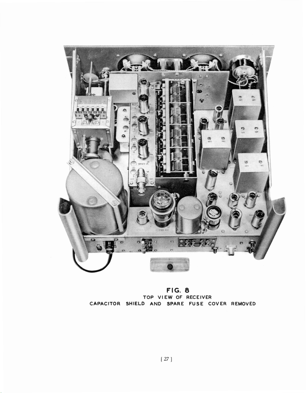
CAPACITOR
SHIELD
TOP
A 0
VI
F
G.
EW
OF RECEIVER
PARE
7 ]
FUSE
COVER
RE
aVED

BOTTOM
TU
leu
FIG
VIEW
IT
9
OF
RECEIVER
SHIELD
[2
]
RE
OVED

R84
RI12
CI44
CI09
R47
R46
R45
SSA
R93
SID
SII
£14
59
r--
m
a::
S8
56
J3
N
ex:
__
e1S8
CI59
R91
,...,-X20
R88
R89
CI60
R92
R86
Xl9
-C151
T7
CI02
S4
£3
£2
CI50
CI69
R70
XI7
CI49
RIOI
R81
CI48
Ra3
XI8
:r~~~~~~lii~~J:i1[~
'.'
~:A~~~~ffi~
C
147
J2
L53
E5
Reo
BOTTOM
VIEW
FIG.
OF
[ 2
10
RECEIVER
SP-600-JX
o
o
u
ex:

SID
C71
C80
C74
C79
R29
R30
SIC
R21
C73
C72
R26
CI54
SIB
RII
C25
RI2
RI14
R6
CI65
15
X2
13--
--L24
R22
C75
L49
R27
C66
CI55
C43
C68
X5
R2
C22
R5
L7
C24
C20
XI
4
SIA
CI9
R2
L48
BOTTO
VIEW
OF
RF
CI53
C21
R3
RI
CI8
R
P
FOR
[ 30 ]

/
BOTTOM
VI
EW
FIG.
Of
fREQUENCY
[31]
12
CONTROL
UNIT

Notes
[ 32 ]
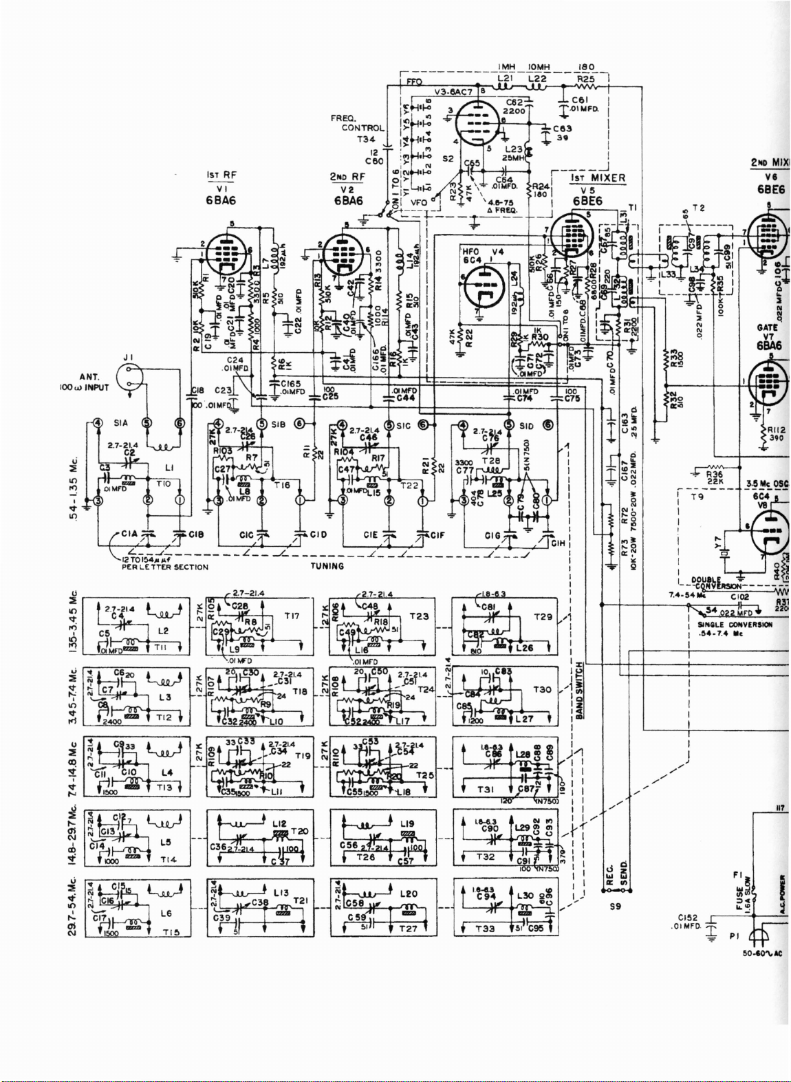
100w
ANT.
INPUT
1ST
RF
VI
6BA6
. R36
22.K
'-;9----
I
I
I
I
...
I >-0
2ND
6BE6
MIXI
VI
CJ
:::E
l()
t·e"lI.4
't"
~
,
C5~
In
Q
...
~
U
:::E
't"
I'-:
I
10
't"
~
u
~
CQ
~
I
v
,..,
~
.....
as
:;;
CI3
~~
C\l
I
Ci4
co
("flOOO
~
U
~
<rf
~
CI6
!~~
In
I
Ci1
.....
as
C\l
n -
I'DIIII
-
~
Til
"-urI
L!5
Tl4
L6
TI!l
~
2 ,
_
Q:
<~
1Z22"
C3~
'--
.CM
I
l_~~,-"
81
T29
""'1
~o
~
TI9
22
_ Q:
~g~
LlI
--
C!5!51
C!5&
T26
~
22
--
T20
'lIS
•
57
L26
T30
L27
..-+-+---_.----":"":"--l~
I
I
1-
....
1~
II
'" J
I~
'4
lID
I
I
I
)/1
I I
I I
I I
I I
I I
I I
I
1....-
....-Vi
I 1
I I
I I
I I
I I
I
.....
1,)
.....
S9
7.4.S4111i
S1NliLE
.S4.?.
I
I
.J
....-"
....-
....-
'"
"
CI02
COHYE"IION
Me
J]
'WV
fiJ
111
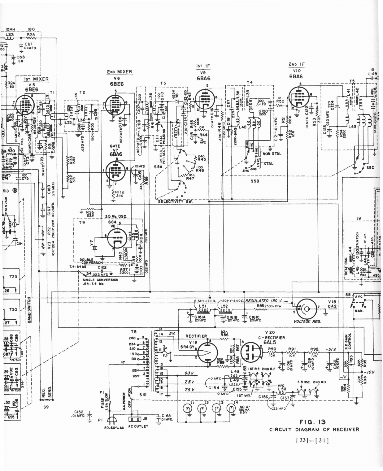
)I~ro
C74
SID
2ND MIXER
V6
68E6
1ST
V9
6BA6
2NO
IF
IF
VIO
6BA6
,-
"
___
-------------
I
I
I
I
I
I
S58
-----
--_/
59
117
50..0,,-AtAC
T8
OUTLET
20HY-440tl.
L52
NEGtlLArEO
R~.2~OO-IOW
+
..,...._CI6IC
~
.20MrO
/50
v.
__
FIG.
13
CIRCUIT OIAGRAM OF RECEIVER
[ 33]-[34-
]

2ND
VIO
SBA6
Vl4
2ND
DEI
a Ave.
IF
51
CI38
~I
CI39
L47
3.0
MH
CI296
.0.!lMFD.
GAL5
VI5
LIMITER a
OUTPUT
METER
GAL5
------------
S58
n
NEGtJLArEO
+
_CI6IC
!
_
20Mro
ISO
R852.!100-IOW
-----
--_/
---
Rill
Cle4
lOOK
430
V
,v.
N£Tt:l'l
ClIO
1D0
ADJ.
11:'"
'"
..,
:
leg
,11:_
I,.."
I
....
,...
11I:"t
I
I"'---r--+I--::"'+::"'::'::'::'::'::'::-:":-:":-:":-:':-:;-;;-:;-:':-:':-:';'::~
11.
__
VOl.TAGE
REG.
vIe
OA2
o F I 0I'l
PHONES
MOD-
u....--<
CW
.......
J
-+-_
57
......
.022
MFO
CI48
-P
~
A.F.
METER
ADJ.
CIRCUIT
FIG.
DIAGRAM
[33]-[
13
OF
34]
ye-,.-"
RECEIVER
~
II:
-/0
V.
ID
m
II:
".F.
AF.
R70
10K
OUTPUT
LEVEL
SW.
RIOI
25K

DIODE
OUTPUT
ANT.
100""
INPUT
.......
t---...,oL-l_-I'-/-/
12~0i~~,-----
P£A
l.£TT£A
ur::~--;:~------,
~
~
I
\()
~
~
'---=~-----'
SECTION
1ST
RF
VI
68A6
__
VI4
2ND
DEI
a Ave.
2NO
1ST
211I0
MIXER
V6
68E6
..,
I
I
I
I
I
I
I
I
I
L
/ / CIG/
__
-L.
-
TUNING
.L
__
.L
.1
../
~I".''''ll
GIH
I
l
I
I
I
I
I
1
. R36
22K
'-;9----
I
I
I
I
V9
68A6
IF
,,;
...
___
I
I
I
J
I
J
S58
e
~
~
m
'1
I
:;I1tt===t=:===--
...
~i
" Jill
Ij
I.
lID
I
I
I
)"1
I I
I I
I I
I I
I 1
I
I
1...-
I
...-r1'
I 1
I I
I I
I I
I I
I
I~)
",'"
"
"
,"
d
0
z
w
w
a::
III
59
I
I
.J
...-"
,
"
FI~
ln~
:;).
"*
'"'~
PI
50.aO,,-AC
CJ52
.0IMfD.
------;-;~~~~~~_+__=~-ill!]S8
T8
117
AC
OUTLET
.511.
7.511.
7..5
+
"'T"_CI6IC
-.!!r
20Mro
V
CIRCUIT
IF
VIO
6BA6
-----
--_/
5/
Cl38
.,
:
leg
I
0:_
,
ro-"
I"",...
I
0:.
r----t---+1f-...:.::..;~::..=...:::..=.::=..:-:.:-:.:-:.:-:.:-~-:.:-:.:-:..::--=-..t::~
.2~..rDC~~O~F~'
..
'
AVe.
MA~
t----.+----I
'-ll---t--"-IOV.
•
PHONES
~
a::
CD
en
It:
FIG.
DIAGRAM
13
OF
vIe
OA2
RECEIVER
I
J
~ON"o-l,......:S:..:7_
"OD-
CW
L.L..-
......
-.+-_4.....J
......
.022
MFO
CI48
~
ft.F.
AF.
"
2
OUTPUT
ft70
10K
LEVEL
sw.
GALS
RIOI
25K
A.F.
METER
VI!!
LIMITER
OUTPUT
METER
GALS
AOJ.
a
[ 33]-[34 ]

MAIN
E3
GREEN-RED
T9
REAR
000
o
()
0 0
OSCILLATOR
TERMINAL
LOCATED
ON
OVER
BOTTOM OF CHASSIS.
13
NOTE:
SWITCHISMOUNTED
ON
TUNING
BY
BANDSWITCH
2-3
CLOSED BELOW 7.4
1-2
CLOSED ABOVE 7.4
BOARD
va
a
V6
BLACK
UNIT
R3B
SOCKETS
[§:H]J:lJ)f"Qj
'-----ll~
OPERATED
MC
MC
T9
FRONT
11'1
II
l.\I
000
o
©
:.
II

'I
~I
MAIN
E3
T9
REAR
000
o
()
0 0
OSCILLATOR
TERMINAL
LOCATED
ON
BOTTOM
BOARD
OVER
V8 a
OF CHASSIS.
NOTE:
SWITCHISMOUNTED
ON
TUNING
BANDSWITCH
BY
2-3
CLOSED BELOW 7.4
1-2
CLOSED ABOVE 7.4
V6
UNIT
SOCKETS
[§"H~~r-lfl
CI28
OPERATED
MC
MC
13
BLACK
CONNECTION
~II
FIGURE
DIAGRAM-REC
NUMB
[3S]
BlA
BlA
BlA
-[
3<:
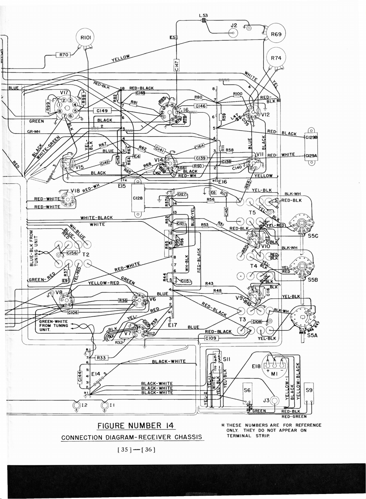
LS3
8
BLACK-WHITE
BLACK-WHITE
BLACK-WHITE
:ll:
I.>
~
:ll:
~
~
~
:r
III
~
II:::
R43
CONNECTION
FIGURE
DIAGRAM-
[3S
NUMBER
RECEIVER
] -
[36]
14
CHASSIS
"*
THESE
ONLY.
TERMINAL
NUMBERS
THEY
DO
STRIP.
ARE
FOR
NOT APPEAR
REFERENCE
ON

MAIN
E3
L53
a
o
CI2
GREEN-RED
T9
REAR
000
o
o 0 0
OSCILLATOR
TERMINAL
LOCATED
ON
BOTTOM
13
NOTE:
ON
BY
2-3
1-2
o
BOARD
OVER
va
OF CHASSIS.
BLACK
SWITCHISMOUNTED
TUNING
BANDSWITCH
CLOSED BELOW 7.4
CLOSED ABOVE 7.4
UNIT
OPERATED
T9
a V6 SOCKETS
~H~h9r-lfl
'----~I~
MC
MC
FRONT
000
o
II II
II
t\I
ll:
I,)
~
:ll:
...J
..J
ID
CD
I
:r
1\
..
~
II::
R43
:.
II
BLACK-WHITE
BLACK-WHITE
BLACK-WHITE
S9
CONNECTION
FIGURE
DIAGRAM-
[ 3S ] - [
NUMBER
RECEIVER
36]
14
CHASSIS
*
THESE
ONLY.
TERMINAL
NUMBERS
THEY
STRIP.
DO
ARE
FOR REFERENCE
NOT
APPEAR
ON

CoN
'l
TO
C60ONFREQUENCY
CONTROL
NOTE:
CLOSEDONPOSITIONS
1-6
SHOWNINVFO
UNIT
THIS
OF
S2.
SWITCH
POSITION.
u
1,1,11,1,1,1,1
YELLOW-BLACK
hl,hhllhl
~u
NOTE:
NUMBERS
SWITCH-BASES
SAMEASTHOSE
ON
SCHEMATIC
GRAM
FOR
AND
SWITCH
COIL
BASES
AND SWITCH
ASSEMBLIES.
ON
ARE
DIA-
BLUE-BLACK
TO
CHASSIS
T2
TERMINAL
18S.
TI
GREEN·WHITE
TO
CHASSIS
EI4
TERMINAL
EI4
TERMINAL
FIGURE
CONNECTION
15
DIAGRAM
TUNING UNIT
TO
R72ONCHASSIS
*
THESE
NUMBERS
8
7
THEYDONOT
ARE
FOR
APPEARONTERMINAL
REFERENCE
ONLY
STRIP

Notes
[
38]
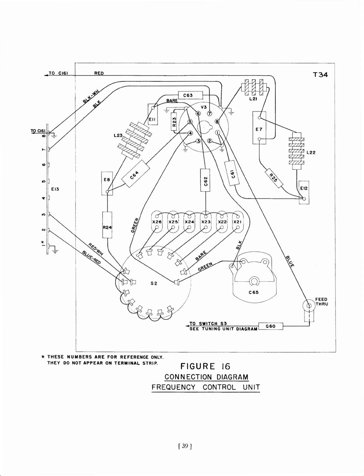
TO CI61
on
EI3
REO
T34
'*
THESE
THEY
NUMBERS
DO
NOT
ARE
APPEARONTERMINAL
FOR REFERENCE ONLY.
TO
SWITCH
SEE
TUNING
STRIP.
FIGURE
CON N ECTION DIAGRAM
FREQUENCY CONTROL
[
39]
S3
UNIT
DIAGRAM,--_C_6_0---,
16
UNIT
C65
FEED
THRU
Notes
October,
lithoinU.S.A. byD.L.
1952-IOM
Terwilliger Co.
SUPPLEMENT A
FOR
INSTRUCTION
MODEL
MODEL
APPLICABLE
TO MODELS
BOOK
ISSUE 4
SP-600-JX
AND
SP-600-J
21
TO
26
460
West
THE
34th
Manufactured
HAMMARLUND
St.
PrintedinU.S.A.
New York
by
MFG.
CO.
1,
INC.
New York,
U.S.A.
FOR
The
modifications
this
signal
signals
supplement
to
noise
up
to
provide
ratios
100-500
The improvement makes
er
satisfactory
direction
Normally
grid
return
connected
terminals
herein).
direction
this
lead
minal
The
of
following
plicable
Book
for
Page 14 -
TABLE
Replace
Page
15 -
finding
to
on
For
finder
to
E13.
to
Models
TUBE
1
TUBE
the
from
the
E13
receiver
the
issue
with
for
equipment.
white-black
Vl
rear
(see
system,
front
changes
4,
SP-600-(21
SOCKEr
page
SOCKEr
RESISTANCE-TABLE
Page
Replace
17 -
INPUT
TABLE
Under
180
100
with
APPROXIMATE
AT
IF&AF
4
APPROX.
microvolts
microvolts.
page
INPUT,
to
USE
WITH
covered
improved
for
microvolts.
the
receiv-
use
with
and V2,
of
tvo
Fig.
use
re-connect
screw
are
Instruction
VOLTAGES
14
herein.
TERMINAL
2
15
herein.
SIGNAL
STAGES
change
read
SUPPLEMENT
MODELS
by
input
lead,
is
screw
15
in
a
ter-
apto
26)
-
-
A
sp-600-
Pages
21
(21
to
TO
24 -
26)
LIST
Replace
with
pages
herein.
Note: T2 -
Gl,
contained
ohms,
This
31116-G2 and
E13.
when making
IF
used
1/2
resistor
This
Transformer
in
earlier
R94,
watt
is
should
replacement
Page 29 - FIG. 10
OF
RECEIVER
Items
Items
Note:
Page 30 - FIG.
RF
Ignore
in
c163,
are
Rl16
c165 and
on
the
Ignore
and R53,
PLATFORM
item
Fig.
R48, R94,
located
front
items
called
11
c165,
II.
Page 33-34 - FIG. 13
GRAM
OF
RECEIVER
Page
Replace
35-36
with
page 33-34
- FIG. 14
DIAGRAM-RECEIVER
Replace
Page
37 - FIG. 15
GRAM-TONING
Replace
Page 39 - FIG.
with
with
page
UNIT
page 37
16
GRAM-FREQUENCY
Replace
vith
page 39
TABLE
21
5 -
PARTS
to
24
- 31116-
models,
Resistor,
1100
- 19309-208BF.
is
omitted
re-located
be
checked
of
BOTl'OM
VIEW
Rl15
on
E13.
R53
are
located
end
of
E17.
c163,
out
BOTrOM
in
VIEW
R48
Fig.
called
CIRCUIT
herein.
CONNECTION
CHASSIS
35-)9
herein.
CONNECTION
herein.
CONNECTION
CONTROL
UNIT
herein.
in
on
T2.
and
10.
OF
out
DIA-
DIA-
DIA-
This
(25
cycles)
Frequency
dications
graphs
erence
Unit,
do
not
and
to
should
apply
The Power
this
model
for
operation
25
cycle
operate
line
frequencies
cycles.
primary
ed.
These
Receiver-Model
does
not
Control
in
the
Unit.
tert,
diagrams,vith
the
Frequency
be
ignored
to
Model
Transformer
is
specially
onasingle
power
line
and
satisfactorily
from 25
Eight
voltage
taps
screw
taps
cover
MODEL
SP-600-J25
have
the
All
photo-
refControl
as
they
sp-600-J.
used
designed
phase
will
on
power
to
terminal
are
provid-
a power
SUPPI.»tENT
FOR
USE
WITH
SP-600-J(25
line
volts.
in-
nected
ped
the
operation
mary
former
former
in
agrees
voltage.
for
60
er,
exceptions
same
respects.
CYCLES)
source
The 117
when
from
the
receiver
make
tap
lead
is
connected
tap
with
The
manufacturer's
the
25
T8,
is
as
Model
range
of
volt
the
receiver
manufacturer.
is
installed
sure
on
the
which
cycle
the
m~st
power
power
31029-3.
this
receiver
sp-600-JX
90
to
tap
that
power
to
the
nearly
source
part
transform-
With
in
270
is
is
for
the
trans-
trans-
number
the
is
all
conship-
When
pri-
above
the

SUPPLEMENT
FOR
USE
WITH
SP-600-JL
Frequency
MODELS
Range--Models SP-600-JL and SP-600-
JLX have a frequency rangeof.100 to .400 me and
1.35 to 29.7mein
Crystal Frequency
not have
in
to
they
Model
the
the
text,
the
Frequency
do not applytoModel SP-600-JL.
SP
Control U nit
In
Position
of
six
bands
.100 to .200
.200to.400
1.35
3.45
7.40 to 14.8
14.80 to 29.7
Control·-
Frequency
photographs
Control
600·
]LX
includes
as described in
as follows:
me
me
to 3.45
me
t07.40mc
me
me
Model SP-600·JL docs
Control
and
Unit. All indications
diagrams, with reference
Unit,
should be ignored as
the
Crystal Frequency
the
text.
DESCRIPTION
AND
SP-600-JLX
Alignmentofthe
With
reference to alignmentofthe
HF
Oscillator, see page 13,
the
for
.100 to .200 me
RF
For the .100 to .200 me
and
adjust Cat.200 me.
For
the
.200 to .400 me
at
and adjust C
Parts List
SP-600-JLX -
23
and
24.
Delete Items
for 54
:0
Delete Items
for 29.7 to 54.0
Add
to Parts List
me
and
.400 me.
Errata
With
TI0,
1.35
me
band).
TIS,
me
band).
.200 to .400mebands:
Amp~r
and
and
Addenda
andHFOscillator -
the
alignment frequencies
.200to.400 me bands are:
band;
AdjustLat
band;
AdjustLat
for SP-600·JL
reference to Table
16,22and
21, 27
the
following, for
and
T28
T33
RF
Amplifier and
.100 me
.200 me
No.5,
(coil assemblies
(coil assemblies
the
.100 to .200
Hammarlund
Part
No.
and
pages
TIO
TI6
T22
T28
TIS
T21
T27
T33
RF
Input
Osc.
Input
Osc.
assembly,
Pt.
shunt
resistor
assembly,
Pt.
assembly,
Pt.
shunt
shunt
resistor
assembly,
Pt.
No.
capacitor
capacitor
Pt.
No.
and
No.
capacitor
capacitor
Pt.
No.
and
capacitor
1stRFTransformer
fixed
2ndRFTransformer
fixed shUht
shunt
HF
capacitor
23071-65, coil
RF
capacitor
1stRFTransformer
fixed
2ndRFTransformer
fixed
shunt
HF
capacitor
23071-66, coil
.100to.200 me,
23063-68C, coil
assembly,
assembly,
No.
.100to.200
23OO3-91C,
switch
.200to.400 me,
23063-68C. coil
assembly,
Pt.
assembly,
No. 19309-182BF
.200to.400 me,
23OO3-90C,
switch
.100to.200
Pt.
No.
23063-68C, coil
.100to.200 me,
Pt.
No.
19309-182BF
me,
102
contacts
.200to.400 me,
No. 23063-68C, coil
.200to.400
Pt.
No.
204
contacts
includesC2trimmer,43mmf
and
switch
contacts
me,
includes
and
2E063-68C, coil, 200,000
and
i!lclu:les C76
mmf
for
includes
and
switch
23063-68C, coil, 200,000
and
includes
mmf
for
SID.
includes
switch
fixed
SID...............................
fixed
trimmer,75mmf
series
CI6
trimmer,43mmf
contacts
includes
and
me,
includes
switch
contacts
C94
trimmer,68mmf
series
. . . . . . . . . . . . . . . . . . . . . . .....
for
C26
switch
C46
contacts
padder
for
C38
switch
C58
padder
[ 3 ]
fixed
SIA.
trimmer,43mmf
contacts
trimmer,43mmf
ohm~watt
for
SIC...........
capJ.citor
SIA.
trimmer,43mmf
contacts
trimmer,43mmf
ohm~watt
for
SIC.
capacitor
shunt
. . . . . . . . . . . 31381-Gl
for
SIB.
fixed
fixed
shunt
Pt.
fixed
shunt
. . . . . . . . . . . . 31334-Gl
for
SIB.
fixed
. . . . . . . . . . 31383-Gl
fixed
shunt
Pt.
No.
. . . . 31382-Gl
. 3138O-G2
3138O-Gl
No.
31379-Gl
. 31383-G2

TUBE
SOCKET VOLTAGES-TABLE 1
Voltagetochassis. Measurements made
were
made
with
asterisk
above 10 volts
and
controlatminimum
TUBE
Y·1
Y·1
Y,2
Y,2
Y·3
Y,3
Y,3
Y·3
Y,4
Y·5
Y,6
Y·6
Y·6
Y,6
Y·7
Y,7
Y·7
Y,7
Y,8
Y,8
Y·9
Y,9
Y,10
Y·10
Y·II
Y·ll
Y,12
Y,12
Y,13
Y,14
Y·15
Y,16
Y,16
Y,17
Y,I7
Y·18
Y,19
Y,19
Y·20
Y,20
1
*-1
*-41
*-1
*-41
-
-
-
- -
130 -
-
-
- -
-
-
*-1
*-54
*-1
*-54
0
30
*-1
*-54
*-1
*-54
*-7.8
*-7.8
-
-
25
-
-
50
57
-
-
150
-
-
-
-
Measurements Corp. Model 62
the
10 volt scale for voltages below 10 volts. Line voltage 117,nosignal input.
and
CW,MOD
2
-
-
-
-
-
-
-
1.2 *6.3ae - 140
-
3
*6.3ae
*6.3ae *6.3ae.
*6.3ae -
-
-
-
- - -
*6.3ae
*6.3ae
*6.3ae
- *6.3ae -
-
-
-
-
-
- *6.3ae
-
-
-
- *6.3ae
-
*6.3ae - 260
*6.3ae
*6.3ae
*6.3ae
*6.3ae
*6.3ae - 30
*6.3ae
*6.3ae -
*6.3ae
- *6.3ae
-
-
-
-
-
-
-
-
*6.3ae
*6.3ae
*6.3ae *6.3ae
*6.3ae
*6.3ae
1.5
1.6
- 260 228
-
-
300
320
*-96
*-97
280
-
-
-
*6.3ae
*6.3ae
with
switchon"CW"
SOCKET
4
5
6
200 95
-
260 245 - -
- 210
260
- -
- -
- -
130 -
-
225 -
-
260 -
-
225
215 125
-
265
-
215
-
265 0
-
-
- 205
260
205
-
- 260 150
-
210
-
235 140
- 210 40
240 45
-
*22
-
-
-
-
265
-
-
-
-
-
25
-
-
-
-
-
150
-
-
-
-
0
95
245
0
150
0
150
110
80
75
245
0
-
- -
90
150
90
140
-
-
-
210
240
-
-
-
-
-
-
-
Weston
Model 663
VTVM.
AVC
PIN
NUMBERS
7 8 9
-
-
*6.3ae
*6.3ae
*6.3ae
*6.3ae
-
-
*-1
*-55
*-1
*-55
304
.4
0
0
- -
-
-
-
-
-
-
-
-
-
-
-
-
-
*6.3ae
*6.3ae
-
-
-
*-96
*-97
The
tap normal.
-
- -
- -
265
265
290
290
-
-
-
-
-
-
-
-
-
-
-
-
-
-
-
-
-
-
-
-
-
-
6
....
7.4 *6.3ae
12
13
-
300
320
-
-
Volt,Ohmmeter,
except those indicated by
500 volt scale was used for all voltages
Audio
-
-
-
-
-
-
-
-
-
-
-
-
-
-
-
-
-
-
--
-
-
-
-
-
-
--
-
-
-
*6.3ae .
-
-
-
-
-
-
-
MODE
RF
Gain max.
RF
Gain min.
RF
Gain max.
RF
Gain min.
RF
Gain
RF
Gain
RF
Gain
RF
Gain
RF
Gain max.ormin.
RF
Gain max.ormin.
RF
Gain
RF
Gain
RF
Gain
RF
Gain
RF
Gain
RF
Gain
RF
Gain
RF
Gain
Frequencies below 704me
Frequencies above
RFGain
RF
Gain min.
RF
Gain max.
RFGain
RFGain
RF
Gain min.
RF
Gain
RF
Gain min.~FO Injection max.
RF
Gain max.ormin.
RF
Gain
RF
Gain max.ormin.
RFGain
RFGain
RFGain
RFGain
RF
Gain max.ormin.
RF
Gain
RF
Gain
RF
Gain max.
RF
Gain min.
OF
OPERATION
max.-YFO
max.-Crystal
min.-YFO
min.-Crystal
max.-Freqs.
min.-Freqs.
max.-Freqs.
min.-Freqs.
max.-Freqs.
min.-Freqs.
max.-Freqs.
min.-Freqs.
7Ame
max.
min.
max.
max.-BFO
max.ormin.
max.
min.
max.
min.
max.-*5
min.-*5YOle
Yae
operation
Freq.
Control
operation
Freq. Control
below
7Ame
below
7Ame
above
7Ame
above
7Ame
below 704me
below 7Arne
above ?o4me
above
7Ame
Injection max.
Pin2to
Pin
2 to
Pin
Pin
Gain
8
8
[ 14 ]

TABLE
No.5
Symbol
Designations
CIA
to
H
C3
C5
C6
C8
C9
Cll
C12
C14
CIS
C17
CIS
C19to24
C25
C27
C29
C30
C32
C33
C35
C37
C39
C40
to
C47
C49
C50
C52
C53
C55
C57
C59
C60
C6l
C62
C63
C64
C65
C66
C67
C68
C69
C70to74
C75
C77
C78
C79
C80
C82
C83
C85
C87
C88
C89
C91
C92
C93
C95
C96
C97
C98
C99
Cl02to104
Cl05
CI06
Cl07
Cl08-l09
ClIO
Clll
C1l2-113
C114
44
DESCRIPTION
Capacitor,
8
Capacitor,
SameasC3
Capacitor,
Capacitor,
Capacitor,
Capacitor,
Capacitor,7mmf
Capacitor,
Capacitor,
SameasCll
Capacitor,
SameasC3
SameasC18
SameasC3
SameasC3
SameasC6
SameasC8
SameasC9
SameasCll
Same
Capacitor,
SameasC3
SameasC3
SameasC3
SameasC6
SameasC8
SameasC9
SameasCll
SameasC18
SameasC39
Capacitor,
SameasC3
Capacitor,
Capacitor,
Same
Capacitor,
SameasC3
Capacitor,
SameasC3
Capacitor,
SameasC3
SameasCIS
Capacitor,
Capacitor,
Capacitor,S
SameasC79
Capacitor,
Ca,pacitor,10mmf
Capacitor,
Capacitor,
SameasC60
Capacitor,
SameasCIS
Capacitor,
Capacitor,
SameasC39
Capacitor,
Capacitor,
Capacitor,
SameasC39
SameasC98
SameasC3
SameasC98
SameasC69
SameasC98
SameasC18
Capacitor,
SameasC18
Capacitor,
sections
as
CIS
as
C3
variable,
.01
mfd
20
mmf
2400
33
mmf
1500
1000
15
mmf.._..23061-l55J
100
mmf
51
mmf
12
mmf
2200
39
mmf
variable
85
:nmf
220
mmf
3300
404
mmf
mmf
810
mmf
1200
120
mmf
190
mmf
51
mmf
379
mmf
610
mmf
65
mmf
.022
mfd
variable
270
mmf
mmf
mmf
mmf
mmf
mmf
mmf
.....
.....
.....
....
.....
....
....
....
....
....
'"
.,.
PARTS
Hammarlund
Part
34001-Gl
_ 23012-1
23003-4lC
23011-40C
23003-45C
230ll-62C
2306l-l68F
230l1-58C
23003-94C
23003-87C
23023-65UJ
23011-17C
23003-47C
ll726-GI09
23071-59
23003-102C
23011-69C
23071-67
23023-8UJ
23072-53
23003-2B
23011-60C
23071-50
23071-64
23023-45UJ
23071-63
23072-52
23071-58
23013-1
11
776-G 1
23003-104C
No.
LIST
Symbol
Designations
C1l5-ll6
C1l7
C1l8
Cll9
C120
C121-122
C123
C124
C125
C126
C127
C128
C129A,
C130
C131
C132
C133
C134
C135
C136
C137
C138-139
C140
C141-142
C143
C144
C145
C146
C147
C148
C149
C150
C151
C152
C153
C156-157
C158
C161A,B,C
C162
C163
C164
C165-166
C167
C168-169
E2
E3
E4-5
E6
E7
E8
E9to12
E13
E14
E15-16
E17
E18
F1
F2
IIto4
J1
B
to
155
to
160
DESCRIPTION
SameasC3
SameasC69
Same
as
Capacitor,
Capacitor,
SameasC3
SameasC98
SameasC69
SameasC1l9
SameasC120
SameasC3
Capacitor,
HS
Capacitor,
HS
Capaci
Capacitor,
SameasC8
SameasC13l
SameasC39
SameasC3
SameasC98
Capacitor,
SameasC92
SameasC131
Capacitor,
Capacitor,
Capacitor,
SameasC15
SameasC98
SameasC143
SameasC98
SameasC143
Capacitor,
800V
SameasC12S
Capacitor,
SameasC3
SameasC98
SameasC128
Capacitor,
450V,
Electrolytic
SameasC98
Capacitor,
SameasC131
SameasC3
SameasC98
SameasC152
4
Screw
Audio
4
Screw
andAVC
1
Solder
(left)
1
Solder
(right)
2
Solder
SameasE4
SameasE6
10
Solder
6
Solder
8
Solder
15
Solder
3
Solder
(meter)
Fuse,
Fuse,
Dial
Mazda
Antenna
UG-103/U
C98
300
1300
10
Can,
Electrolytic.
2 x .05
Can,
Paper
tor,27mmf
430
.25
100
5100
.05
2500
.01
3 x 20
HS
.25
Terminal,
Output
Terminal,
Terminal
Terminal
Terminal
Terminal
Terminal
Terminal
Terminal
Terminal
1.6A
Fusetron
%
Amp
Lamp,
input
Can,
No.
mmf
mmf
mfd,
100V
mfd,
mmf
mfd,
200V
mmf
mmf
mfd
mmf,
mfd
500V 23072-11
mfd,
mfd,
600V
Diode
strip
strip
strip.
Board
strip.
strip.
strip
strip
47
socket,
Hammarlund
Part
23003-105C
23011-61C
15462-1
15461-1
23023-71 U J
23003-109C
2391l-79E
23024-24SL
23015-16A
23911-77E
23070-40
15463-1
23915-1
31141-1
31480-1
16650-9
16650-11
16650-12
33928-G1
16650-10
31163-G1
31162-Gl
31454-G1
15893-1
15928-13
16004-1
_.._ 15959-1
No.
[21]

PARTS
LIST
(Continued)
Symbol
Designations
J2
J3
J5
L7
L14
L21
L22
L23
L24
L35
L46
L47
L48
L49-50
L51
L52
L53
M1
PI
P2
P3
P4
R1
R2
R3
R4
R5
R6
R7-8
R9
R10-11
R12
R13
R14
R15
R16
R17-18
R19
R20-21
R22-23
R24-25
R26
R27
R28
R29-30
R31
R32
DESCRIPTION
IF
Output
SO-239
Phone
Power
RF
192
SameasL7
RF
Choke,1millihenry.
RF
10
RF
25
SameasL7
SameasL7
RF
12
RF
3.0
RF
Choke,2ohms
RF
1st
Filter
170
2nd
440
IF
Output
Tuning
Power
Antenna
UG-102/U
Antenna
Connector
Cable
PL-259
Resistor,
1/3
Resistor,
1/
2
Resistor,
I/
Z
Risistor,
V2
Resistor,
1/
2
SameasR4
Resistor,
1/
2
Resistor,
V2
Resistor,
I/
Z
Same
Same
SameasR3
Same
Same
SameasR7
SameasR9
SameasRIO
Resistor,
1/
2
Resistor,
1/
2
SameasR1
Resistor,
1/
2
Resistor,
112
SameasR4
Resistor,
V2
SameasR5
Socket,
Jack,
receptacle
Choke,
microhenries
Choke,
millihenries
Choke,
millihenries
Choke,
microhenries
Choke,
millihenries
Choke,
Filter
watt
watt
watt
Choke,
ohms
ohms
Meter
plug
Input
Adapter
Connector
(for
510K
watt
10K
watt
33K
watt
1000
watt
510
watt
51
watt
24
watt
22
watt
as
R2
as
Rl
as
R5
as
R4
47K
watt
180
watt
150
6800
2200
2.7
dc
Choke,20Hy,
dc
transformer.
JK-34-A
and
....
dc
ohms
8.5
cord
Plug,
UG-104/U.
Plug
J2)
ohms
ohms
ohms
ohms
ohms
ohms
ohms
ohms
ohms
ohms
ohms
ohms
ohms
.
.
.
....
.
.
dc.
Hy,
.
.
.
..
.
.
.
.
.
.
.
.
.
.
.
.
.
.
.
Hammarlund
Part
No.
16111-1
5066-1
35013-1
15612-G1
15617-G1
15618-1
15619-1
15615-2
15616-G1
15611-1
15613-1
31030-2
31031-2
31488-1
4903-2
6143-1
16016-1
15987-1
16071-1
19317-76BF
19309-278BF
19309-282BF
19309-49BF
19309-170BF
19309-193BF
19309-189BF
19309-9BF
19309-89BF
19309-31BF
19309-259BF
19309-69BF
19309-57BF
Symbol
Designations
R33
R35
R36
R37
R38
R39
R40
R41
R42
R43
R44
R45
R46
R47
R48
R49
R50
R51
R52
R53
R54
R55
R56
R57
R58
R59
R60-61
R62
R63
R64
R65
R66
R67-68
R69
R70
R72
R73
R74
R75-76
R77
R78
R79
R80
R81
R82
R83
R84
R85
R86
R87-88
R89
DESCRIPTION
Resistor,
112
Resistor,
l/
R~i:s~:tt
Same
SameasR35
SameasR3
Resistor,
1
SameasR31 I
Resistor,
l/
SameasR35
SameasR2
Resistor,
l/
Resistor,
V2
Resistor,
112
Resistor,1megohm
1fz
SameasR31
SameasR42
SameasR35
SameasR2
SameasR2
SameasR31
SameasR42
SameasR35
SameasR2
SameasR31
Resistor,
1
SameasR48
SameasR35
Resistor,
l/
SameasR22
SameasR36
SameasR47
SameasR35
Resistor,
3300
SameasR2
Resistor,
R;~s~~~t
20
Resistor,
1000
SameasR35
SameasR22
Resistor,
1/
Resistor,
1/
SameasR31
SameasR35
SameasR2
SameasR4
Resistor,
500K
Resistor,
10
Resistor,
1/
Resistor,
1/
SameasR86
1500
watt
lOOK
watt
Z
2~~
as
R31 I
20K
watt
10
watt
Z
240
watt
Z
1100
watt
18K
watt
watt
2200
watt
27K
watt
Z
variable
ohms.
7500
Hii{
watt
variable
ohms.
470K
watt
2
680
2
watt
variable
ohms
2500
watts
82K
watt
2
120K
watt
2
ohms
ohms
..
~~~.s
ohms
ohms
ohms
ohms
ohms
ohms
ohms
. .... . ...15366-1
ohms
'~h~;'"
. . . . . . ...15363-1
ohms
ohms
ohms
ohms
ohms
Hammarlund
Part
!19309-53BF
I
19309-97BF
·1
19309-178BF
i
1
,
"
19310-179BF
I
i
19309-1BF
II
I 19309-201
I
19309-208BF
i
i
19309-79BF
I
19309-121BF
I
.
I
19310-57BF
.
!
19309-83BF
i
'
.119397-41
19397-43
II
19309-113BF
'I
19309-45BF
!
15342-11
.
19396-1
.
\
19309-287BF
.
I
19309-181BF
No.
BF
I 22 ]
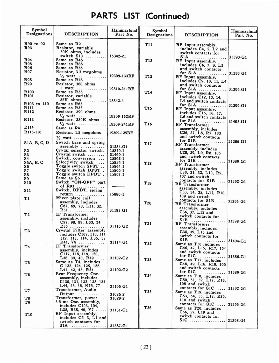
PARTS
LIST
(Continued)
Symbol
Designations
R90to92
R93
R94
R95
R96
R97
R98
R99
RI00
R101
RI03
to
RIll
R112
R113
R114
RI15-116
SIA,
B,C,
S2
S3
S4
S5A,B,C
S6
S7
S8
S9
S10
SI1
Tl
T2
T3
T4
T5
T6
T7
T8
T9
TI0
SameasR2
Resistor,
SameasR46
SameasR86
SameasR36
Resistor,
1/
SameasR78
Resistor,
SameasR35
Resistor, variable
110
25K
SameasR63
SameasR35
Resistor,
1f2
Resistor,
1f2
SameasR4
Resistor.
~
Switch
D
Cry
Crystal
Switch,
Selectivity
Toggle
Toggle
Toggle
SameasS6
Switch
of
Switch,
return
Mixer
assembly,
C67, 69, 70,
R31 .
IF
assembly,
R35
Crystal
R41,
IF
assembly,
C117,
L38,
SameasT4,
C 123, 124, 125, 126,
L41,
Beat
assembly,
C130, 131, 132, 133, 134
L44, 45, 46,
Transformer,
Output
Transformer,
3.5
includes
L35,
RF
includes
switch
SIA
DESCRIPTION
50K
switch
1
assembly
C97, 98, 99,
includes
112, 113, 114,
variable
ohms,
S10 .
3.3
watt
2
360
watt
ohms
390
watt
330K
watt
1.5
watt
base
tal
selector
switch
conver-sion
switch
switch
switch
switch
"ON-OFF"
R93
DPDT,
plate
includes
Transformer
Transformer
Frequency
me
Input
includes
Filter
CI07,
Y8
includes
118,119,120,
39, 40,
42, 43,
includes
Osc.
assembly,
CI03,
R38,
40,
assembly,
C2, 3,Lland
contacts
megohms
megohms
and
coil
includes
Audio
includes
ohms
ohms
ohms
spring
switch.
SPST
DPST
DPDT
spring
L31,
L33,
assembly
110,111
L36,
R49
R54
Osc.
R76,
77
power
104,
Y7
for
.
.
.
.
..
.
.
part
.
.
32,
34
.
37
.
....
....
..
.
..
.....
, .
Hammarlund
Part
15342-21
.
19309-133BF
.
19310-211BF
.
15342-4
.
19309-162BF
.
19309-241BF
19309-125BF
31234-Gl
15879-1
31469-1
15862-1
15856-1
15864-1
15866-1
15867-1
15880-1
31183-Gl
31116-G2
31114-Gl
31102-G2
31102-G2
31106-Gl
31086-2
31029-2
31131-Gl
31387-G1
No.
Symbol
Designations
Tll
T12
T13
T14
TIS
T16
T17
T18
T19
T20
T21
T22
T23
T24
T25
T26
DESCRIPTION
RF
Input
includes
switch
SIA
RF
includes
and
for
RF
includes
and
for
RF
includes
L5
for
RF
includes
L6
for
RF
assembly,
C26, 27,
and
for
RF
assembly,
C28, 29,
and
for
RF
assembly,
C30, 31, 32,
107
contacts
RF
assembly,
C33, 34, 35,
109
contacts
RF
assembly,
C36, 37,
switch
SIB
RF
assembly,
C38, 39,
switch
SIB
SameasT16
C46, 47,
and
for
SameasT17,
C48, 49,
and
for
SameasT18,
C50, 51, 52,
108
contacts
SameasT19,
C53, 54, 55,
110
contacts
SameasT20,
C56, 57,
switch
SIC
assembly,
contacts
Input
assembly,
switch
SlA
Input
assembly,
switch
SIA
Input
assembly,
and
switch
SIA
Input
assembly,
and
switch
SIA
Transformer
switch
SIB
Transformer
L9,
switch
SIB
Transformer
and
switch
Transformer
and
switch
Transformer
L12
contacts
Transformer
L13
contacts
switch
SIC
switch
SIC
and
and
contacts
C4, 5,L2and
for
C6, 7, 8,
C9, 10, 11,
C12, 13, 14,
CIS,
includes
L8,
contacts
includes
contacts
includes
for
includes
for
includes
includes
includes
LIS,
contacts
L16,
contacts
switch
for
switch
for
L19
contacts
contacts
contacts
16, 17,
contacts
R7,
103
R8,
105
LI0,
SIB
Lll,
SIB
and
for
and
for
R17, 104
includes
R18, 106
includes
L17,
SIC
includes
L18,
SIC
includes
and
for
L3
R9,
....
RIO,
....
R19,
....
R20,
....
Hammarlund
31390-G1
31393-Gl
L4
31396-Gl
31399-Gl
31405-Gl
31386-G1
31389-Gl
31392-Gl
31395-G 1
31398-Gl
31404-Gl
31386-Gl
31389-Gl
31392-Gl
31395-Gl
31398-Gl
Part
No.
[23]

PARTS
LIST
-Continued
Symbol
Designations
T27
T28
T29
T30
T31
T32
T33
T34
XI-2
X3
X4
X5
X6to15
X16
X17
X18
X19
X20
X21to26
Ylto6
DESCRIPTION
SameasT21,
C58,
59,
switch
SIC
HF
includes
L25
contacts
HF
includes
and
for
HF
includes
L27
contacts
HF
includes
89,
contacts
HF
includes
93,
contacts
HF
includes
L30
contacts
Crystal
includes
63, 64, 65,
L21,
X3,21to
Tube
Tube
Tube
ceramic,
shield
Tube
ceramic,
shield
SameasXl
Tube
SameasX3
SameasXl
SameasX3
SameasXl
Crystal
for
Crystal,
note
Osc.
and
Osc.
switch
SID
Osc.
and
Osc.
L28
Osc.
L29
Osc.
and
control
22, 23,
socket,
socket,
socket,
socket,
socket,
crystals
below
contacts
assembly,
assembly,
assembly,
assembly,
assembly,
and
assembly,
socket,
CR-18/U,
includes
L20
and
for
C76, 77, 78,
switch
for
SID
C81, 82,
contacts
C83, 84, 85,
switch
for
SID
C86, 87, 88,
and
switch
for
SID
C90, 91, 92,
switch
for
SID
C94, 95, 96,
swi
tch
for
SID
assembly,
C60, 61, 62,
E7.
8, 11, 12,
R23,
24, 25,
26
miniature.
octal
miniature
less
center
miniature
with
center
noval
ceramic,
YltoY6.
see
....
L26
....
....
....
.....
...
" 16100-1
Hammarlund
Part
31404-Gl
31385-Gl
31388-Gl
31391-Gl
31394-Gl
31397-Gl
31403-Gl
31409-Gl
15989-4
16082-1
15989-5
15989-3
16092-5
31473-spec
No.
Symbol
Designations
Y7
Y8
Miscellaneous
DESCRIPTION
Crystal,
Crystal,
Chart,
Dial,
Dial,
Dial,
Dial,
Fuse
Knob
Knob
Knob
Knob
Knob
Knob
Knob,
Knob,
Knurled
Shaft
Shaft
Shaft
Snap
Spare
Spring,
Spring,
Spring,
Spring,
Spring,
Spring,
Spring,
Spring,
Window,
Window,
Wrench,
6 11806-2
Wrench,
8 11806-3
Wrench,
3.5
me
455
kc
frequency
band
indicator
Lamp
assembly
Gain)
Freq.
Phasing)
Gain)
(Selectivity)
soft
stiff
Detent
Switch
grounding
Coils
Coil
10 11806-4
Socket
main
tuning
vernier
Holder
and
and
and
and
and
and
frequency
tuning
Coupling,
Coupling,
Coupling,
Button
fuse
assemblies
tuning
Dial
Dial
Osc.)
Dial
Dial
Dial
Skirt
lock
thumb
Plug
cover
anti-blacklash
Band
Change
Conversion
Crystal
IF
adjuster
Indicator
Retainer
Retainer
Band
Tuning
Set
Screw
Set
Screw
Set
Screw
(Audio
(Beat
(Crystal
(RF
(large).
screw
rigid
flexible
flexible
Retaining
Indicator
control
control
.....
Slide..
for
for
Dials.
No.
No.
No.
...
..
"
..
RF
RF
.
31130-1
.
31471-1
31463-1
31201-Gl
31453-1
.
31438-1
.
.
31439-1
15923-1
.
31227-G2
31227-G4
31227-G3
31227-Gl
.
31227-G5
31215-Gl
31434-Gl
31462-Gl
31495-1
31275-Gl
.
.
.
29619-2
.
31494-1
31239-1
31205-1
31125-1
31417-1
31023-1
31126-1
31004-1
.
31003-1
31282-1
31281-1
Hammarlund
Part
No
415-G3
415-G2
NOTE:
Hammarlund
Crystal
made
CR-18/U.
plusorminus
ance
00.75000to07.39999
07.40000on3.45to7.40
07.40000on7.40to14.8
07.40001to12.04499
12.0450
44.0450
NOTE:
which
double
occursatthe
Frequency
in
accordance
with
to
tc
the
conversion
Crystals
Specification
The
frequency
.005%.
HC-6/U
Signal
44.04499
54.00000
Since
intermediate
high
supplied
Control
with
or
Fuquency
7.40
and
frequency
No.
Unit,
Signal
tolerance
The
holder
CR-7.
band
band
meISthe
frequency
since
endofthe
on
31473,
see
MC
signal
this
soecial
for
page8,shall
Corps
Specification
shall
shallbein
frequency
is
changed
signal
3.45to7.40
order,
useinthe
be
within
accord-
0.455000
0.455000
3.955000
3.955000
3.955000
3.955000
frequency
per
for
mc
[ 24 ]
be
The
Signil]
used
shallbestampedonthe
The
~iven
signal
following:
Add
IF
Frequency
(see
note
(see
and
and
at
below)
note
below)
divide
divide
band
and
14.8mcband,itis
as
wellasSignal
for
exactly
Frequency
oscillator
frequency
sumby3
sumby4
alsoatthe
7.40mcsignal
for
which
topofthe
or
actual
MC
low
necessarytospecify
Frequency
crystal
shall
frequency
operation.
be
determined
ModeofOperation
when
the
crystalisto
holder.
frequency
Fundamental
Fundamental
Fundamental
Fundamental
3rd
Harmonic
4th
Harmonic
endofthe
frequency
ordering
for
from
7.40
crystals
be
a
the
to
band

1ST
RF
VI
6BA6
2-
68£6
MIXER
va
L--J--------L
~£W~t'f,.~
~r-----,
SECTION
__
-L
TUNING
~
__
J J J
ZIO
1M
110
T8
.to
130
"7

1ST
v.
68A6
2ND
IF
IF
VIO
6BA6
elG~
;'
._J
• I
W
Lt'
/ic
•
elM
J
T29
'1
:
m:111
~:il
ltl
T31
---::.;....,
......
l!-..f:"d-:
l&oU
c.c
T32
Lt-U.. I I
Gf4
T33
I
I
I...,
1 I
I I
.1
:
I
I I
I
I"
A'r
I t
...
\ 1
I I
I 1
....'
....
'
CIIl6
-
.0IM"D
I
I
",,'
,,/
,...
,...
....
" r----'I"-'IT
d
~
"
~
.01
CJ52
liFO.
F~!
~~
r-:---=-t";===t=l----,
..,..=!::.
PI
...L
!lO.ecn.1C&COUTLET
RII2
390
~
II
.....
~.DIMF1l.
I
I
t
I
I
__
-I
MEG
RII!I
1.!>MtG
A48
1.0
NORMAL
~------...,,'--'V'IWI,....~
CIS8
-----
1'118
I.5MtG
OF
FIG.
CIRCUIT
DIAGRAM
--_/
13
OF RECEIVER
[33]-[
34}
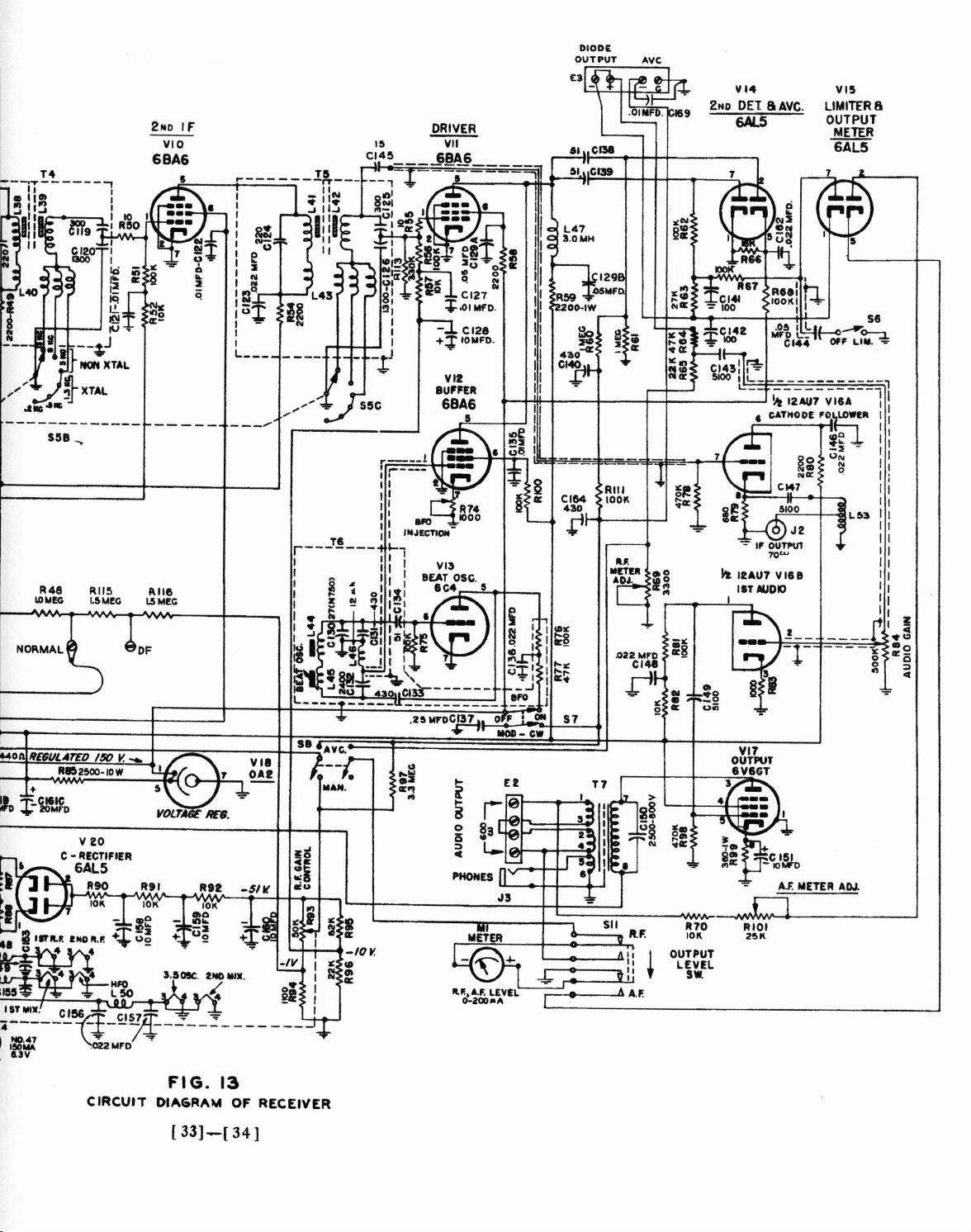
DIDDlE
OUTPUT
'we
\/14
2"0 DEl a
6Al5
Ave.
VI!!
LIMITER
OUTPUT
METER
6AL5
6
R48
LOMEG
NORMAd~
MOll fI£6ULATED
_-t-_<y"\l\.!'M2_$OO.....;-10.;..w;.;....
~C:6":E~fIEII
:a,
..
~Il
]
i.,[~7
~
!')
111'11.
;.ltiii·,.,..U
-..
~
,15'~
liT
••.
' C
t-l:L
J-.Jl
1!16.~'--'
V
1190
RII!!
1.!IMtG
/50
20
10K
~:
V.
_ l,
__
I
-4-;e
+~
MFO
L.~
Dn
~
'"""
i.l.H-t'
.,/'
n'
!I\\.'-'
1191
10K
2 + U
2
•
~
J
VOI.T11r
10.
11.2
.~K
jll:~~
o
_
5,llOSC, ZItDIlII..
58
V
II
"
~
~
-51"
~~
.;r.
~
/ • I .
~4
_
""e.
I)
l--r;-
1I"1f.
~I
c,.
'"
~!
..
,-+_1;-"_101'.~'"
:!!...
2_.
- "
'--t===::~J~'
~
!
:-1" -
II
~
ell!
N;
_ +
......
.,2
a::",
...
i
[2
~
B r
o
83
U
is
•
~~
u..._++--+--J
"E!!!IlT'EII
-
~
"'''.'''.
LE"EL
0-200."
-e~.-....'
_.-
-e.oo~D=:::jF=;;':::
~
~
+ .,J;..r---_---..
A------;Y-l-~~-~--~-------
.':.:1
1.3"
\:022
MFD
VI7
OUTPUT
IVIGT
T7l
::
~
=t!:~·~~~-~~.--,j~.&n---L-
---
....
,---------------
:
'-~
*~~:
,i
"
Sit
....
v
1lF.
:,:
v
•
•.
> 4 -
S§
'---t--~
u
OUTPUT
I LEVEL
F.
lr;~
".I-,\to+-r'.
-
"_
.:-Jt.
~
i!
1170 RIO'
10K
sw.
--.
I
yCJaJo
-
AF.
2!1K
IIIlETER
AD./.
-.J
--1
CIRCUIT
FIG.
OIAGRAU
[33]-[
la
OF
34]
RECEIVER
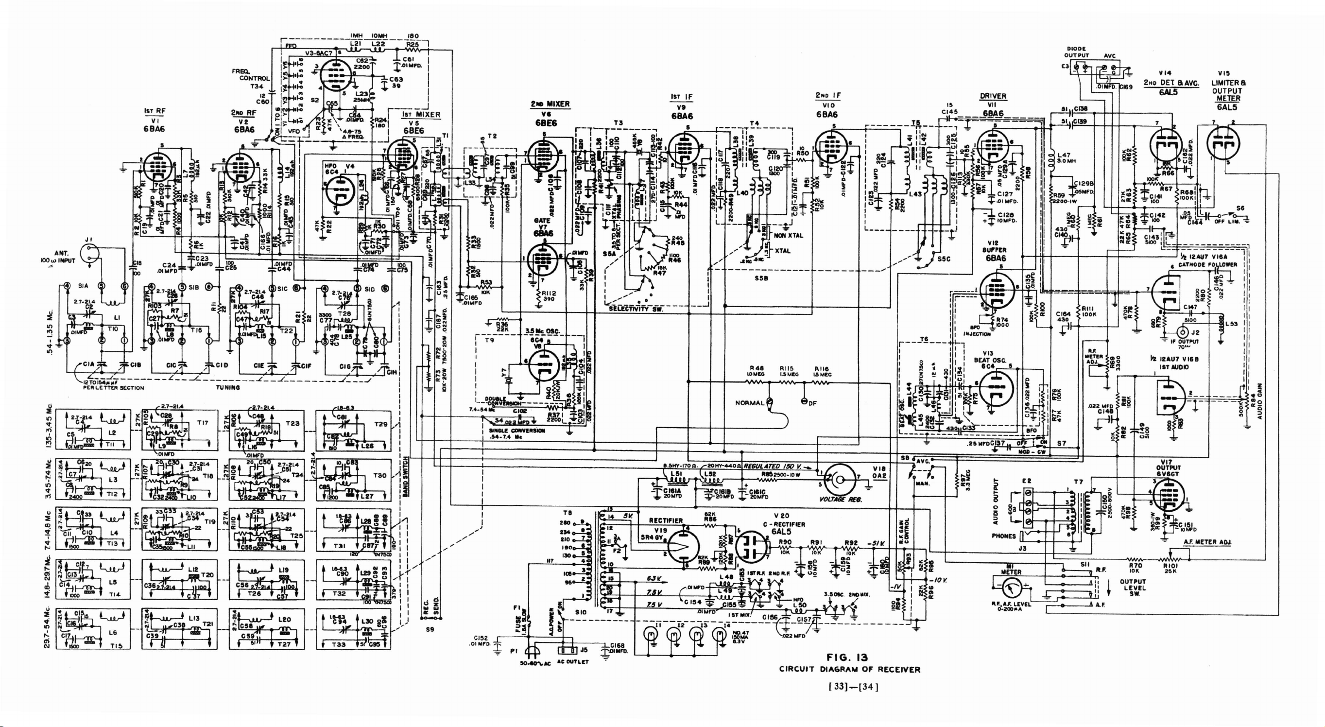
1ST
RF
VI
6BA6
FAB4
CONTROl.
T34
lIT
VI
6SA6
\/14
2ND
DEl8Ave.
2ND
IF
\/10
6BA6
IF
1$
.1
CI3lI
$1
CI3I
6AlS
VIS
LIMITER
OUTPUT
METER
6AL5
8
ANT.
IOOwlMPuT
~~I~~7---
PtllLtTTDlStCTION
~,..------,
L-_-L
TUNING
12
- -
en
T20
~
~
I~~
6 C3
c
n
Ll3
121
---
C5.
~
__~__
•
T21
L..._
J J J I
..........._ ......
...JcIHI
12.
'
110
~
L-:.=:..---!....::.::;~....:...J
L...-_-
~;!j~EHA'r
,.... I t
~----''flQ'w.;Dd
L21
.......
"L-~::cd-
.1
.. I :
I
'"
I
I
I
I
I
I
I
I
1
I
I
I
I
I
I
~1
I
I
I
I
JI:
I·
1°
:1
I
I
'....,
I I
I I
:
l I
I
I
I
1,-
I I
I I
I I
,I"~
59
....
"'2
a:,
¥
g
CI~
.Ollotr'O
10K
$O..ecn.ac
Cl28
+
..
10.,'0.
VII
IU'ftlt
6BA6
-------------
I
I
I
I
I
-----
--_/
I
---'
-""
A48
ID.,&
I!J()
OF
V.
_
R9I
It,2
10K
.0
-
Ill.
+
o~
FIG.
DIAGRAMOFRECEIVER
13
VII
OA2
-511/
+~
AYe;,
IIAN.
u
•
~~
IE,,!
...
~
i
~
~
0
is
:>
c
NO"MAL
.~-_=::::-::-:-::_:+==__====_=_:_;_-+-::;;;;;:::_---_++s:.:.:....;
liT
Cl18
AC
OUTLET
~.otMFO.
REfJULATED
CIRCUIT
0'
1MlD-
II
I'
I
I
S
C CI&4
ON
I
t.
4)0
S7
-V
h1
s
Rtll
lOOK
II.F.
M!nll
AD'"
.022lot'D
Sit
II:
•
CI48
~
It.F.
II
II
II
I
•.
~
F.
...0
"
.a
"n
=:
.0
lf~
...
-"
=~
..
•
a:
!!
"
OUTPUT
LEVEL
1170
lOll
a.
•
!8
00;
CI4,i
5100 I
It
~
L_
-----------~
1.:_
~~;-~7-
• tATNODt
IUU7
VI18
liT
.,010
§ "
U METER
1t101
251l
;I;;--l
'Ofi
!;
0",
0
'"
L"
----f
AOJ.
I
I
I
-
r
I
I
I
I
I
II
II
II
II
, I
'I
I
I
I
I I
I c
.1:1
·0
lEo
0
"
0
:>
..
c
(33]-[34
]

E3
ORANGE-GRN
T9
REAR
O'
0 0
o
© 0 0
OSCILLATOR
TERMINAL
LOCATED
ON
OVER
BOTTOM OF CHASSIS.
NOTE:
SWITCH IS
ON
TUNING
BY
BANDSWITCH
2-3
CLOSED BELOW 7.4
1-2
CLOSED ABOVE 7.4
BOARD
VB6V6
MOUNTED
UNIT
OPERATED
T9
FRONT
SOCKETS
~tffi:@fD.J
MC
MC
13
BLACK

L53
BLACK
o
CI2
CONNECTION
FIGURE
DIAGRAM-
[ 35 ] - [ 36 ]
BLACK-
WHITE
BLACK-WHITE
BLACK-WHITE
NUMBER
RECEIVER
14
CHASSIS
*THESE
ONLY.
TERMINAL
NUMBERS
THEY
00
STRIP.
ARE
FOR
NOT APPEAR
REFERENCE
ON
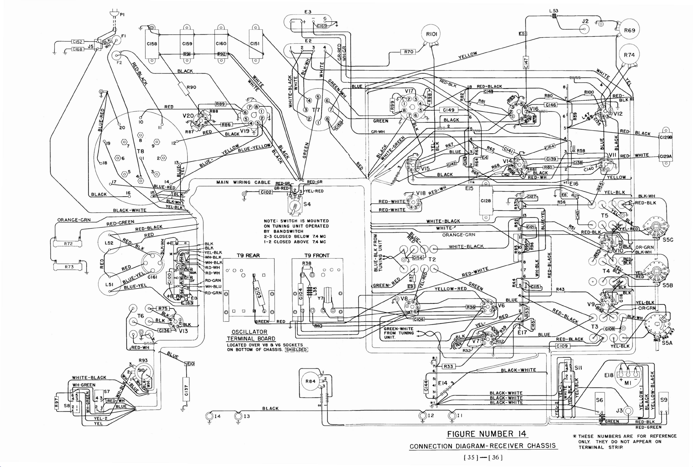
E3
L53
BLACK
ORANGE-GRN
T9
REAR
O' 0 0
o
© 0 0
OSCILLATOR
TERMINAL
LOCATED
ON
OVER
BOTTOMOFCHASSIS.
13
NOTE: SWITCH IS MOUNTED
ON
TUNING
BY
BANDSWITCH
2-3
CLOSED BELOW 7.4
1-2
CLOSED ABOVE 7.4
UNIT
OPERATED
T9
BOARD
VB
a V6 SOCKETS
~H~hP.fDJ
L.---~lll
BLACK
MC
MC
FRONT
o 0 0 I
o
II't
II
N
:I
II
BLACK-WHITE
BLACK-WH
BLACK-WHITE
ITE
CONNECTION
FIGURE
DIAGRAM-
[35]-(36)
NUMBER
RECEIVER
14
CHASSIS
*
THESE
ONLY THEY
TERMINAL
NUMBERS
DO
STRIP.
ARE
FOR REFERENCE
NOT
APPEAR
ON
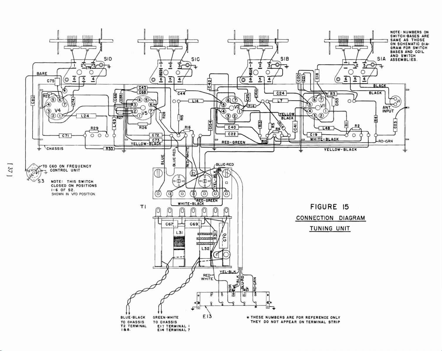
NOTE: NUMBERS
,:
SWITCH-BASES
!
SAMEASTHOSE
ON
SCHEMATIC DIA-
GRAM
FOR
BASES AND
AND SWITCH
ASSEMBLIES.
ARE
SWITCH
COIL
ON
T
TO
W
~~~
'J
C60ONFREQUENCY
CONTROL
NOTE:
CLOSEDONPOSITIONS
1-6OF52.
SHOWNINVFO
UNIT
THIS
SWITCH
POSITION.
TI
YELLOW-BLACK
FIGURE
15
CONNECTION DIAGRAM
BLUE-BLACK
TO
CHASSIS
T2
TERMINAL
1818.
GREEN'WHITE
TO
CHASSIS
EI7
TERMINAL
EI4
TERMINAL
TUNING
EI3
I
7
,.,
THESE
NUMBERS
THEYDONOT
ARE
FOR
APPEARONTERMINAL
REFERENCE ONLY
UNIT
STRIP

BLK-WH
T
Cl61
TO
CI61
eo
RE
L22
T34
!
*"
-0
o e
Jl!
THESE
THEY
OlD
NUMBERS
DO
NOT
ARE
FOR REFERENCE ONLY.
APPEARONTERMINAL
TO SWITCH
SEE
TUNING
STRIP.
FIGURE
CON N ECTION DIAGRAM
FREQUENCY CONTROL
S3
UNIT
16
C65
DIAGRAM
UNIT
C60
FEED
THRU
[
39]

 Loading...