HAMAMATSU S3901, S3904 Service Manual

查询S3901供应商
IMAGE SENSOR
NMOS linear image sensor
S3901/S3904 series
Current output, high UV sensitivity, excellent linearity, low power consumption
NMOS linear image sensors are self-scanning photodiode arrays designed specifically as detectors for multichannel spectroscopy. The scanning
circuit is made up of N-channel MOS transistors, operates at low power consumption and is easy to handle. Each photodiode has a large active
area, high UV sensitivity yet very low noise, delivering a high S/N even at low light levels. NMOS linear image sensors also offer excellent output
linearity and wide dynamic range.
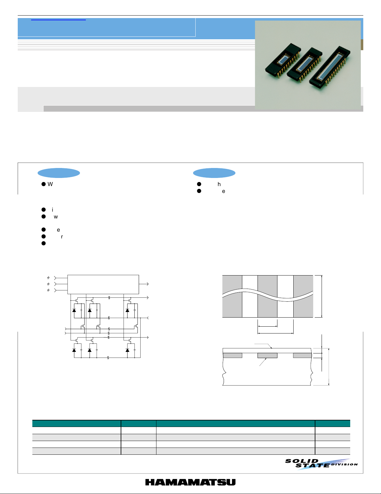
The photodiodes of S3901 series have a height of 2.5 mm and are arrayed in a row at a spacing of 50 µm. The photodiodes of S3904 series also
have a height of 2.5 mm but are arrayed at a spacing of 25 µm. The photodiodes are available in 3 different pixel quantities for each series: 128
(S3901-128Q), 256 (S3901-256Q, S3904-256Q), 512 (S3901-512Q, S3904-512Q) and 1024 (S3904-1024Q). Quartz glass is the standard window
material.
Features
l
Wide active area
Pixel pitch: 50 µm (S3901 series)
Pixel height: 2.5 mm
l
High UV sensitivity with good stability
l
Low dark current and high saturation charge allow a long
integration time and a wide dynamic range at room temperature
l
Excellent output linearity and sensitivity spatial uniformity
l
Lower power consumption: 1 mW Max.
l
Start pulse and clock pulses are CMOS logic compatible
Figure 1 Equivalent circuit
START st
CLOCK
CLOCK12
ACTIVE
PHOTODIODE
SATURATION
CONTROL GATE
SATURATION
CONTROL DRAIN
DUMMY DIODE
25 µm (S3904 series)
DEGITAL SHIFT RESISTER
(MOS SHIFT RESISTER)
END OF SCAN
ACTIVE VIDEO
Vss
DUMMY VIDEO
Applications
l
Multichannel spectrophotometry
l
Image readout system
Figure 2 Active area structure
b
OXIDATION SILICON
2.5 mm
a
1.0 µm
■
Absolute maximum ratings
KMPDC0020EA
S3901 SERIES: a=50 µm, b=45 µm
S3904 SERIES: a=25 µm, b=20 µm
N TYPE SILICON
P TYPE SILICON
1.0 µm
KMPDA0059EA
Parameter Symbol Value Unit
Input pulse (φ1, φ2, φst) voltage V
Power consumption *
Operating temperature *
1
2
Topr -40 to +65 °C
φ
P 1 mW
15 V
Storage temperature Tstg -40 to +85 °C
*1: Vφ=5.0 V
*2: No dew
400 µm

Shape specifications
)
)
■
NMOS linear image sensor
S3901/S3904 series
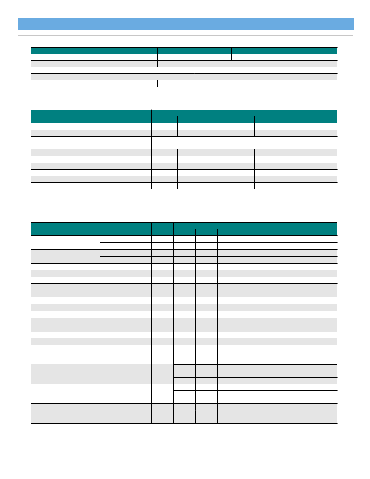
Parameter S3901-128Q S3901-256Q S3901-512Q S3904-256Q S3904-512Q S3904-1024Q Unit
Number of pixels 128 256 512 256 512 1024 -
Package length 31.75 40.6 31.75 40.6 mm
Number of pins 22 22 Window material *
3
Quartz Quartz -
Weight 3.0 3.5 3.0 3.5 g
*3: Fiber optic plate is available.
Specifications (Ta=25 °C)
■
Parameter Symbol
S3901 series S3904 series
Min. Typ. Max. Min. Typ. Max.
Pixel pitch - - 50 - - 25 Pixel height - - 2.5 - - 2.5 - mm
Spectral response range
(10 % of peak)
Peak sensitivity wavelength
Photodiode dark current *
Photodiode capacitance *
Saturation exposure *4, *
4
4
5
Saturation output charge *
λ
p
λ
I
D
Cph - 20 - - 10 - pF
4
Esat - 180 - - 180 - mlx · s
Qsat - 50 - - 25 - pC
200 to 1000 200 to 1000 nm
- 600 - - 600 - nm
- 0.2 0.6 - 0.1 0.3 pA
Photo response non-uniformity *6PRNU - - ±3 - - ±3 %
*4: Vb=2.0 V, Vφ=5.0 V
*5: 2856 K, tungsten lamp
*6: 50 % of saturation, excluding the start pixel and last pixel
Unit
m
µ
■
Electrical characteristics (Ta=25 °C)
Parameter Symbol
Clock pulse (φ1, φ2)
voltage
Start pulse (φst) voltage
Video bias voltage *
7
High
Low
High
Low
Condition
Vφ1, Vφ2 (H)
Vφ1, Vφ2 (L)
Vφs (H)
Vφs (L)
Vb 1.5
S3901 series S3904 series
Min. Typ. Max. Min. Typ. Max.
4.5 5 10 4.5 5 10 V
0-0.40-0.4 V
4.5
Vφ1
10 4.5
Vφ1
10 V
0 - 0.4 0 - 0.4 V
Vφ - 3.0 Vφ - 2.5
1.5
Vφ - 3.0 Vφ - 2.5
Saturation control gate voltage Vscg - 0 - - 0 - V
Saturation control drain voltage Vscd - Vb - - Vb - V
trφ1, trφ2
Clock pulse (φ1, φ2) rise / fall time *
Clock pulse (φ1, φ2) pulse width tpwφ1, tpwφ2
Start pulse (φst) rise / fall time trφs, tfφs
Start pulse (φst) pulse width tpwφs
Start pulse (φst) and clock pulse
(φ2) overlap
Clock pulse space *
Data rate *
9
8
Clock pulse (φ1, φ2)
line capacitance
Saturation control gate (Vscg)
line capacitance
*7: Vφ is input pulse voltage (refer to figure 8).
*8: trf is the clock pulse rise or fall time. A clock pulse space of
input if the clock pulse rise or fall time is longer than 20
8
tfφ1, tfφ2
tφov
X1, X
f 0.1 - 2000 0.1 - 2000 kHz
C
Cscg 5 V bias
- 20 - - 20 - ns
200 - - 200 - - ns
- 20 - - 20 - ns
200 - - 200 - - ns
200 - - 200 - - ns
2
50 % of
saturation
*
5 V bias
φ
2 V bias
V
trf - 20 - - trf - 20 - - ns
-
9, *10
-
-
-
-
-
-
-
-
-
-
-
rise time/fall time - 20 ns (nanoseconds) or more should be
ns (refer to figure 7).
80 (-128 Q)
120 (-256 Q)
160 (-512 Q)
21 (-128 Q)
36 (-256 Q)
67 (-512 Q)
12 (-128 Q)
20 (-256 Q)
35 (-512 Q)
7 (-128 Q)
11 (-256 Q)
20 (-512 Q)
--
--
--
- -
- -
- -
--
--
--
- -
- -
- -
100 (-256 Q)
150 (-512 Q)
200 (-1024 Q
27 (-256 Q)
50 (-512 Q)
100 (-1024 Q
14 (-256 Q)
24 (-512 Q)
45 (-1024 Q)
10 (-256 Q)
16 (-512 Q)
30 (-1024 Q)
-ns
-nsVideo delay time tvd
-ns
- pF
- pF
- pF
-pF
-pF
-pF
- pF
- pFVideo line capacitance C
- pF
*9: Vb=2.0 V, Vφ=5.0 V
*10: Measured with C7883 driver circuit.
Unit
V
 Loading...