

HAMAMATSU R3896 Datasheet
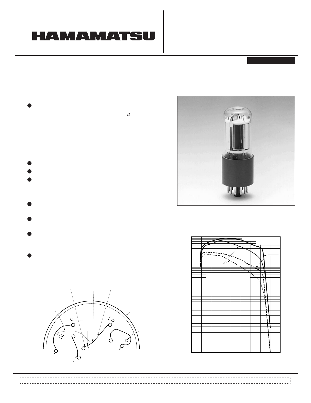
High Q.E Multialkali Photocathode
28mm (1-1/8 Inch) Diameter, 9-Stage, Side-On Type
FEATURES
High Sensitivity
Luminous ..........................................
Radiant
at 450nm (peak) .............................
at 633nm .........................................
Quantum Efficiency
at 260nm (peak) ....................................
at 633nm (peak) ....................................
Wide Spectral Response ............................
High Signal to Noise Ratio
Newly Designed Electro Optical Structure
PHOTOMULTlPLlER TUBE
R3896
PATENT PENDING
New Electro–Optical Design
525 A/lm (Typ.)
90mA/W (Typ.)
73mA/W (Typ.)
30% (Typ.)
14% (Typ.)
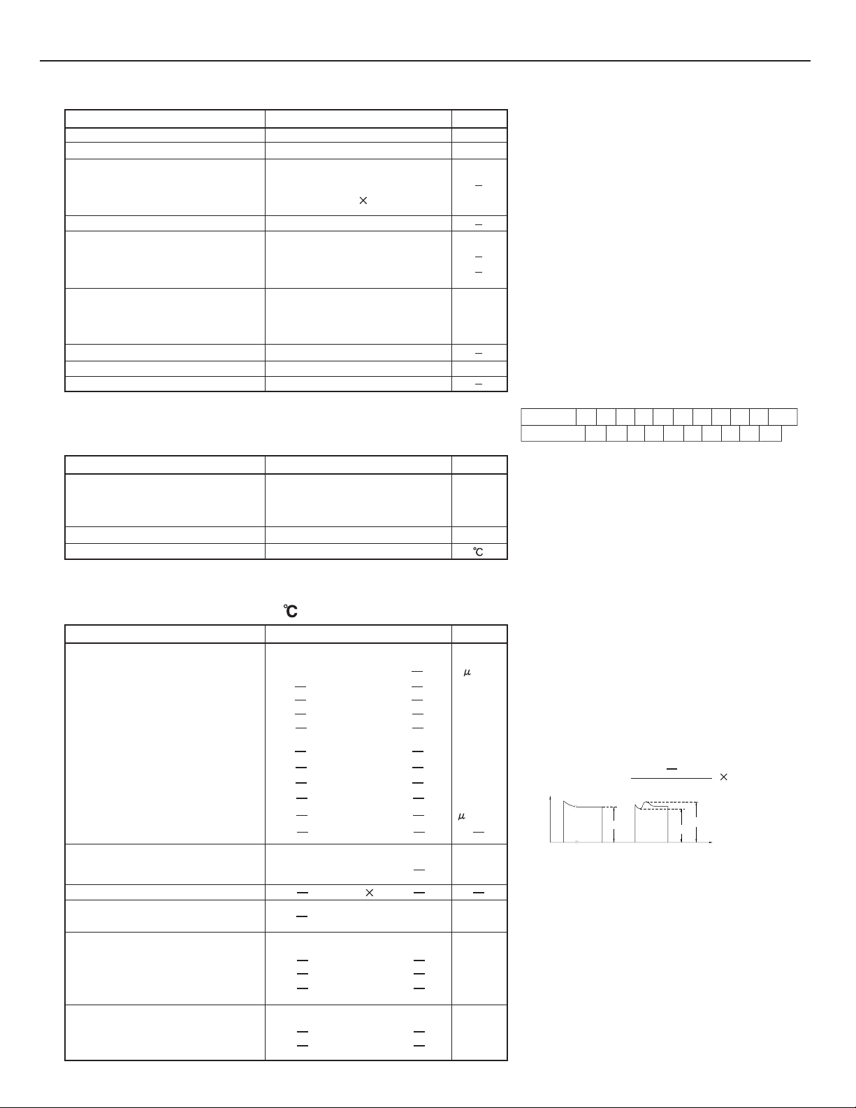
185 to 900nm
APPLICATIONS
Biomedical Analysis
Blood Analyzer, Flow Cytometer, DNA Sequencer
Environmental Monitoring
NOx Analyzer
Spectroscopy
Fluorescence Spectrometer, Raman Spectrometer,
UV–VIS Spectrometer
Semiconductor Industry
Wafer Inspection, Particle Counter
Figure 1: Electro Optical Structure
LIGHT
PHOTOELECTRON
TRAJECTORIES
GRILL
GLASS BULB
ANODE
Figure 2: Typical Spectral Response
TPMSB0049EB
100
R928
10
QUANTUM EFFICIENCY
1
QUANTUM EFFICIENCY (%)
0.1
CATHODE RADIANT SENSITIVITY (mA/W)
CATHODE RADIANT
SENSITIVITY
R3896
1st DYNODE
PHOTOCATHODE
2nd DYNODE
Subject to local technical requirements and regulat ions, availability of products included in this promotional material may va r y. Please consult with our sales office.
lnformation furnished by HAMA M ATSU is believed to be reliabIe. However, no responsibility is assumed for possibIe inaccuracies or ommissions. Specifications are
subject to change without notice. No patent right are granted to any of the circuits described herein.
9th DYNODE
TPMSC0024EA
0.01
100 200 300 400 500 600 700 800 900 1000
WAVELENGTH (nm)
1994 Hamamatsu Photonics K.K.
©
PHOTOMULTlPLlER TUBE R3896
GENERAL
Parameter Description/Value Unit
Spectral Response
Wavelength of Maximum Response
Photocathode
MateriaI
Minimum Effective Area
Window Material
Dynode
Structure
Number of Stages
Direct Interelectrode Capacitances
Anode to Last Dynode
Anode to All Other Electrodes
Base
Weight
SuitabIe Socket
185 to 900 nm
450
Multialkali
8 24
UV glass
Circular-cage
9
4pF
6pF
JEDEC No. B11-88
Approx. 45
E678–11A (option)
MAXIMUM RATINGS (Absolute Maximum Values)
Parameter Value Unit
Supply Voltage
Between Anode and Cathode
Between Anode and Last Dynode
Average Anode Current
A
Ambient Temperature
1250
250
0.1
–80 to +50
CHARACTERISTlCS (at 25 )
Parameter Typ.Min. Max. Unit
Cathode Sensitivity
Luminous
Radiant at 254nm
Quantum Efficiency at 254nm 29.3
Blue
Red/White Ratio
Anode Sensitivity
Luminous
Gain
Anode Dark Current
(after 30min. storage in the darkness)
Time Response
Anode Pulse Rise Time
Electron Transit Time
Transit Time Spread (TTS)
Anode Current Stability
Current Hysteresis
Voltage Hysteresis
B
475
525
60
450nm
633nm
852nm
450nm
633nm
852nm
C
D
E
E
F
G
H
I
J
3000 5000
90
73
5.0
24.8
14.3
0.73
15
0.4
9.5 10
2.2
22
1.2
6
5010
0.1
1.0
nm
mm
g
Vdc
Vdc
mA
A/lm
mA/W
mA/W
mA/W
mA/W
%
%
%
%
A/lm-b
A/lm
nA
ns
ns
ns
%
%
NOTES
A:
Averaged over any interval of 30 seconds
maximum.
B:
The light source is a tungsten filament lamp
operated at a distribution temperature of 2856K.
Supply voltage is 100 volts between the cathode
and all other electrodes connected together as
anode.
C:
The value is cathode output current when a blue
filter(Coming CS-5-58 polished to 1/2 stock
thickness) is interposed between the light source
and the tube under the same condition as Note B.
D:
Red/White ratio is the quotient of the cathode
current measured using a red filter(Toshiba R-68)
interposed between the light source and the tube
by the cathode current measured with the filter
removed under the same conditions as Note B.
E:
Measured with the same light source as Note B
and with the voltage distribution ratio shown in
Table 1 below.
Table 1:Voltage Distribution Ratio
Electrodes K Dy1 Dy2 Dy3 Dy4 Dy5 Dy6 Dy7 Dy8 Dy9 P
Ratio
SuppIy Voltage : 1000Vdc, K : Cathode, Dy : Dynode, P : Anode
F:
Measured with the same supply voltage and
voltage distribution ratio as Note E after removal of
light.
G:
The rise time is the time for the output pulse to
rise from 10% to 90% of the peak amplitude when
the entire photocathode is illuminated by a delta
function light pulse.
H:
The electron transit time is the interval between
the arrival of delta function light pulse at the
entrance window of the tube and the time when
the anode output reaches the peak amplitube. In
measurement, the whole photocathode is
illuminated.
I:
Also called transit time jitter. This is the fluctuation
in electron transit time between individual pulses in
the signal photoelectron mode, and may be defined
as the FWHM of the frequency distribution of
electron transit times
J:
Hysteresis is temporary instability in anode current
after light and voltage are applied.
ANODE
CURRENT
(1)Current Hysteresis
The tube is operated at 750 volts with an anode
current of 1 microampere for 5 minutes. The light is
then removed from the tube for a minute. The tube is
then re-illuminated by the previous light level for a
minute to measure the variation.
(2)Voltage Hysteresis
The tube is operated at 300 volts with an anode
current of 0.1 micro-ampere for 5 minutes. The light
is then removed from the tube and the supply voltage
is quickly increased to 800 volts. After a minute, the
supply voltage is then reduced to the previous value
and the tube is re-illuminated for a minute to
measure the variation.
1111111111
l
l
max.
Hysteresis = 100(%)
l
i
5 6 7 (minutes)
0
min.
l
i
l
max.
l
min.
TIME
TPMSB0002EA
 Loading...