

HAMAMATSU R375 Datasheet
PHOTOMULTIPLIER TUBE
R375
160 to 850 nm Response (Multialkali)
51 mm (2 Inch) Diameter, 10-stage, Head-On Type
GENERAL
Parameter Description/Value Unit
Spectral Response
Wavelength of Maximum Response
Photocathode
Window Material
Dynode
Base
Suitable Socket
Material
Minimum Effective Area
Structure
Number of Stages
160 to 850
420
Multialkali
46
Synthetic Silica
Box and Grid
10
15-pin glass base
E678-15B (supplied)
nm
nm
—
mm dia.
—
—
—
—
—
MAXIMUM RATINGS (Absolute Maximum Values)
Parameter Value Unit
Supply Voltage
Average Anode Current
Ambient Temperature
Between Anode and Cathode
Between Anode and Last Dynode
CHARACTERISTICS (at 25 °C)
Parameter Min. Unit
Luminous (2856 K)
Cathode Sensitivity
Anode Sensitivity
Gain
Anode Dark Current (after 30 min storage in darkness)
Time Response
NOTE: Anode characteristics are measured with the voltage distribution ratio shown below.
Radiant at 420 nm
Red/White Ratio (R-68)
Luminous (2856 K)
Radiant at 420 nm
Anode Pulse Rise Time
Electron Transit Time
80
—
—
20
—
—
—
—
—
VOLTAGE DISTRIBUTION RATIO AND SUPPLY VOLTAGE
Electrodes
Ratio
Supply Voltage: 1000 V dc, K: Cathode, Dy: Dynode, P: Anode
K G Dy11Dy21Dy31Dy4 Dy51Dy61Dy7
11
1500
250
0.1
-80 to +50
Typ. Max.
150
64
0.2
80
3.4 × 10
5.3 × 10
11111
4
5
5
9.0
70
Dy8 Dy9 Dy10 P
—
—
—
—
—
—
20
—
—
V dc
V dc
mA
°C
µA/lm
mA/W
—
A/lm
A/W
—
nA
ns
ns
Subject to local technical requirements and regulations, availability of products included in this promotional material may vary. Please consult with our sales office.
Information furnished by HAMAMATSU is believed to be reliable. However, no responsibility is assumed for possible inaccuracies or omissions. Specifications are
subject to change without notice. No patent rights are granted to any of the circuits described herein.
2001 Hamamatsu Photonics K.K.
©
PHOTOMULTIPLIER TUBE R375
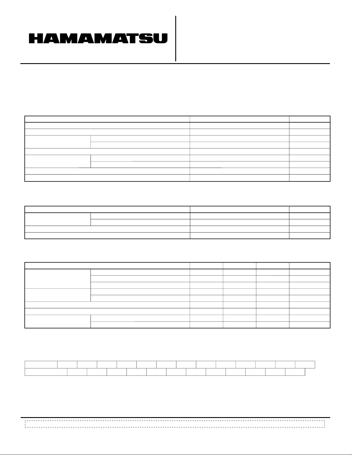
Figure 1: Typical Spectral Response
TPMHB0643EA
100
10
QUANTUM
EFFICIENCY
1
QUANTUM EFFICIENCY (%)
0.1
CATHODE RADIANT SENSITIVITY (mA/W)
0.01
200 800600400
WAVELENGTH (nm)
CATHODE
RADIANT
SENSITIVITY
1000
Figure 2: Typical Gain Characteristics
TPMHB0598EA
7
10
6
10
5
10
GAIN
4
10
3
10
2
10
500 600 700 800 1000
SUPPLY VOLTAGE (V)
1200
1400
Figure 3: Dimensional Outline and Basing Diagram (Unit: mm)
51.0±1.5
FACEPLATE
PHOTOCATHODE
46MIN.
15 PIN BASE
112±2
13MAX.
DY10
DY8
IC
DY6
IC
P
6
5
4
3
2
DY4
SHORT PIN
DY9
DY7
8
9
7
1
15
DY2
10
11
12
13
14
G
TPMHA0211EA
DY5
DY3
K
DY1
Socket
(E678-15B)
60
50
4
45
40
5
2
11.5
40
5
TACCA0201EA
HAMAMATSU PHOTONICS K.K., Electron Tube Center
314-5, Shimokanzo, Toyooka-village, Iwata-gun, Shizuoka-ken, 438-0193, Japan, Telephone: (81)539/62-5248, Fax: (81)539/62-2205
U.S.A.:
Hamamatsu Corporation: 360 Foothill Road, P. O. Box 6910, Bridgewater. N.J. 08807-0910, U.S.A., Telephone: (1)908-231-0960, Fax: (1)908-231-1218 E-mail: usa@hamamatsu.com
Germany:
Hamamatsu Photonics Deutschland GmbH: Arzbergerstr. 10, D-82211 Herrsching am Ammersee, Germany, Telephone: (49)8152-375-0, Fax: (49)8152-2658 E-mail: info@hamamatsu.de
France:
Hamamatsu Photonics France S.A.R.L.: 8, Rue du Saule Trapu, Parc du Moulin de Massy, 91882 Massy Cedex, France, Telephone: (33)1 69 53 71 00, Fax: (33)1 69 53 71 10 E-mail: infos@hamamatsu.fr
United Kingdom:
North Europe:
Italy:
Hamamatsu Photonics UK Limited: 2 Howard Court, 10 Tewin Road Welwyn Garden City Hertfordshire AL7 1BW, United Kingdom, Telephone: 44-(0)1707-294888, Fax: 44(0)1707-325777 E-mail: info@hamamatsu.co.uk
Hamamatsu Photonics Norden AB: Smidesvägen 12, SE-171-41 SOLNA, Sweden, Telephone: (46)8-509-031-00, Fax: (46)8-509-031-01 E-mail: info@hamamatsu.se
Hamamatsu Photonics Italia: S.R.L.: Strada della Moia, 1/E, 20020 Arese, (Milano), Italy, Telephone: (39)02-935 81 733, Fax: (39)02-935 81 741 E-mail: info@hamamatsu.it
HOMEPAGE URL http://www.hamamatsu.com
TPMH1246E03
OCT. 2001 IP
 Loading...