

HAMAMATSU R212 Datasheet
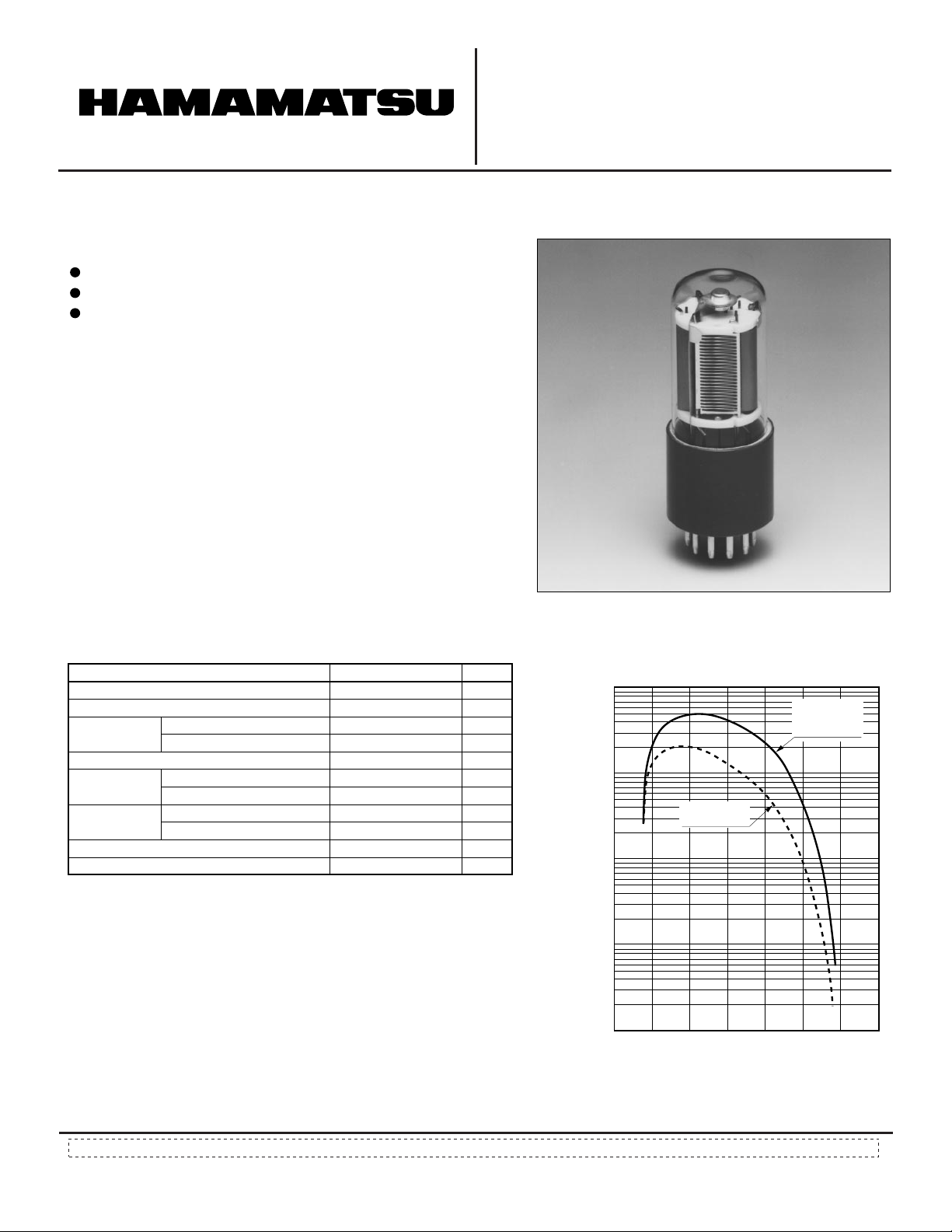
FEATURES
28mm (1-1/8 Inch) Diameter Side-on
185 to 650nm Spectral Response
High Gain and Low Dark Current Variant of 1P28
PHOTOMULTIPLIER TUBE
R212
GENERAL
Parameter Description/value Unit
Spectral Response
Wavelength of Maximum Response
Photocathode
Window Material
Dynode
Direct
Interelectrode
Capacitances
Base
Suitable Socket
Material
Minimum Useful Size
Structure
Number of Stages
Anode to Last Dynode
Anode to All Other Electrodes
185 to 650
340
Sb-Cs
8 × 24
UV glass
Circular-cage
9
4
6
JEDEC No. B11-88
E678-11A
nm
nm
—
mm
—
—
—
pF
pF
—
—
Figure 1: Typical Spectral Response
100
10
QUANTUM
EFFICIENCY
1
QUANTUM EFFICIENCY (%)
0.1
CATHODE RADIANT SENSITIVITY (mA/W)
0.01
200 400 600 800
WAVELENGTH (nm)
CATHODE
RADIANT
SENSITIVITY
Subject to local technical requirements and regulat ions, availability of products included in this promotional material may var y. P lease consult with our sales office.
Information furnished by HAMA M ATSU is believed to be reliable. However, n o responsibility is assumed for possible inaccuracies or omissions. Specifications are
subject to change without notice. No patent rights are granted to any of the circuits described herein.
1998 Hamamatsu Photonics K.K.
©
PHOTOMULTIPLIER TUBE R212
MAXIMUM RATINGS (Absolute Maximum Values)
Parameter Value Unit
Between Anode
Supply
Voltage
and Cathode
Between Anode
and Last Dynode
Average Anode Current
Ambient Temperature
1250
250
0.1
-80 to +50
Vdc
Vdc
mA
°C
CHARACTERISTICS (at 25°C)
Parameter Typ.Min. Max. Unit
—
—
—
—
—
—
—
—
10
—
—
A/lm
A/W
A/W
µA/lm
mA/W
mA/W
%
—
nA
ns
ns
Anode
Sensitivity
Luminous (2856K)
Radiant
Luminous (2856K)
Cathode
Sensitivity
Radiant
Quantum Efficiency
Gain
Anode Dark Current
Time
Response
Anode Pulse Rise Time
Electron Transit Time
at 340nm
at 254nm
at 340nm
at 254nm
(after 30minutes)
50
—
—
25
—
—
—
—
—
—
—
300
3.6 × 10
3.0 × 10
40
48
40
20
at 270nm
7.5 × 10
2.2
22
5
5
6
1
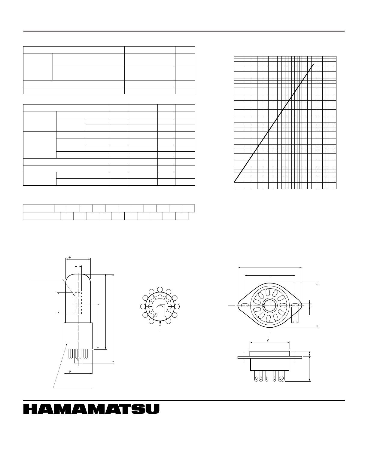
VOL TAGE DISTRIBUTION RA TIO AND SUPPLY VOLTAGE
Electrodes
Ratio
Supply Voltage: 1000Vdc, K: Cathode, Dy: Dynode, P: Anode
K Dy11Dy21Dy31Dy41Dy51Dy61Dy71Dy81Dy91P
1
Figure 2: Typical Gain Characteristics
TPMSB0144EA
8
10
7
10
6
10
5
10
GAIN
4
10
3
10
2
10
250 300 400 700 1000 1500 2000
SUPPLY VOLTAGE (V)
Figure 3: Dimensional Outline and Basing Diagram
(Unit: mm)
28.5 ± 1.5
8MIN.
PHOTOCATHODE
DY5
5
DY4
4
3
24MIN.
32.2 ± 0.5
11 PIN BASE
JEDEC No. B11-88
80MAX.
49.0 ± 2.5
94MAX.
DY3
2
DY2
1
DY1
DIRECTION OF LIGHT
Socket (Option)
(E678-11A)
49
38
DY6
DY7
6
7
DY8
8
9
DY9
10
P
11
K
29
TPMSA0001EA TACCA0064EA
5
33
3.5
4
18
HAMAMATSU PHOTONICS K.K., Electoron Tube Center
314-5, Shimokanzo, Toyooka-village, Iwata-gun, Shizuoka-ken, 438-0193, Japan, Telephone: (81)539/62-5248, Fax: (81)539/62-2205
U.S.A.:
Hamamatsu Corporation: 360 Foothill Road, P. O. Box 6910, Bridgewater. N.J. 08807-0910, U.S.A., Telephone: (1)908-231-0960, Fax: (1)908-231-1218
Germany:
Hamamatsu Photonics Deutschland GmbH: Arzbergerstr. 10, D-82211 Herrsching am Ammersee, Germany, Telephone: (49)8152-375-0, Fax: (49)8152-2658
France:
Hamamatsu Photonics France S.A.R.L.: 8, Rue du Saule Trapu, Parc du Moulin de Massy, 91882 Massy Cedex, France, Telephone: (33)1 69 53 71 00, Fax: (33)1 69 53 71 10
United Kingdom:
North Europe:
Italy:
Hamamatsu Photonics UK Limted: Lough Point, 2 Gladbeck Way, Windmill Hill, Enfield, Middlesex EN2 7JA, United Kingdom, Telephone: (44)181-367-3560, Fax: (44)181-367-6384
Hamamatsu Photonics Norden AB: Färögatan 7, S-164-40 Kista Sweden, Telephone: (46)8-703-29-50, Fax: (46)8-750-58-95
Hamamatsu Photonics Italia: S.R.L.: Via Della Moia, 1/E, 20020 Arese, (Milano), Italy, Telephone: (39)2-935 81 733, Fax: (39)2-935 81 741
TPMS1041E01
JUN. 1998
 Loading...