HAMAMATSU L7141-10, L7140-10 Datasheet

LED/PHOTO IC
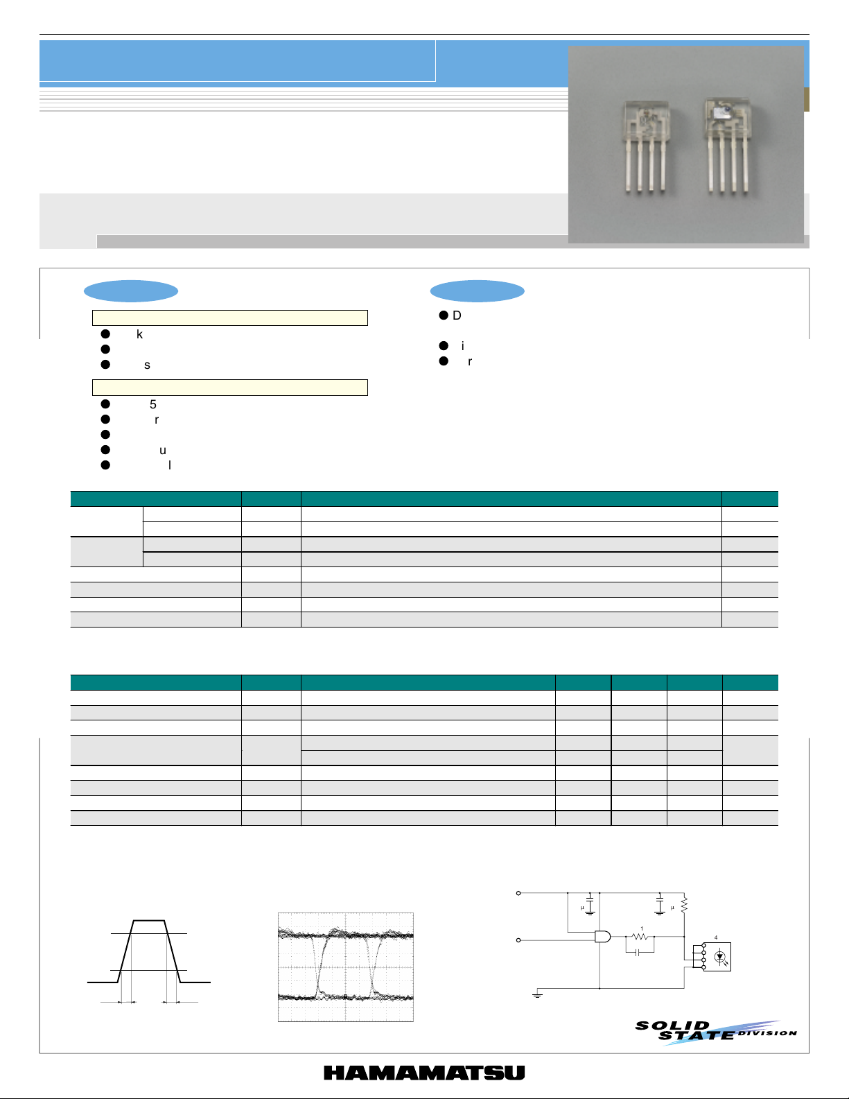
Red LED/Photo IC for optical link
L7140-10/S7141-10
For 50 Mbps optical link
Features Applications
l
L7140-10
l
Peak emission wavelength: 650 nm
l
High output power
l
High-speed response
S7141-10
l
DC to 50 Mbps data transmission
l
Miniature size due to monolithic IC structure
l
Designed to be used with L7140-10
l
Digital output
l
Inversion logic
■ Absolute maximum ratings (Ta=25 °C)
Parameter Symbol Value Unit
L7140-10
S7141-10
Power dissipation *
Reverse voltage V
Forward current I
Power supply Vcc -0.5 to +7 V
Output current Ioh 10 mA
Operating temperature Topr -10 to +70 °C
Storage temperature Tstg -40 to +85 °C
Soldering - 230 °C, 5 s, at least 1.5 mm away from package surface *1: Derate power dissipation at a rate of 1.75mW /°C above Ta=25 °C
4
.
P 250 mW
Data transmission in FA or OA applications subject to large
amounts of electro magnetic noise
l
High-speed, short distance data transmission
l
Burst data transmission
5V
40 mA
■ Electrical and optical characteristics (L7140-10) (Ta=25 °C)
Parameter Symbol Condition Min. Typ. Max. Unit
Data rate f
Forward voltage V
Reverse current I
Fiber coupled optical power Po
Peak wavelength
Spectral half width (FW HM)
Rise time at pulse drive tr I.=20 mA, driven by recommended circuit *
Fall time at pulse drive tf I.=20 mA, driven by recommended circuit *
*2: Output from a 1 meter long plastic fiber (GH4001 made by Mitsubishi Rayon) set close to the m olded lens.
*3: Output optical waveform is defined by the waveform shown below.
■ Output optical waveform
definition
80 %
20 %
tr
tf
KLEDC0015EB
,
Driven by recommended circuit DC - 50 Mbps
.
I.=20 mA - 1.9 2.3 V
4
V4=5 V - - 10 µA
I.=10 mA *
I.=20 mA *
.
I
l
Dl
p
=20 mA - 650 - nm
I.=20 mA - 20 - nm
■ L7140-10 output optical
waveform example
5 ns/div.
KLEDC0019EA
-10 - -
-7 - -
!
--8ns
!
- - 8 ns
■ Drive circuit example
(R1=300 Ω, R2=750 Ω, C1=77 pF)
Vcc
0.1 mF 0.1 mFR2
74ACT08
14
SIGNAL INPUT
* This is merely an example of drive circuit and not for actual large-
volume production purposes.
1
2
R1
3
7
C1
1
2
3
4
dBm
L7140-10
KLEDC0014EB

Red LED/Photo IC for optical link
L7140-10/S7141-10
■ Electrical and optical characteristics (S7141-10) (Ta=25 °C)
Parameter Symbol Condition Min. Typ. Max. Unit
Data rate f
,
Supply voltage Vcc 4.75 - 5.25 V
Current consumption Icc Without light input - - 32 mA
Pulse width distortion
Minimum overload Pimax *" *
Minimum receiver input power Pimin *" *
Rise time tr *
Fall time tf *
Output voltage
,T
Voh Ioh=20 µA 2 - - V
Vol Io l= -0.6 mA *
#
#
#
#
$
*4: Output from a 1 meter long plastic fiber (GH4001 made by Mitsubishi Rayon) set close to the molded lens.
*5: Evaluated based on the input/output waveforms shown below. Measured with a low-capacitance FET probe (3 pF or less).
*6: Output is the L level (inversion logic) when light is input.
DC 50 Mbps
-6 - +6 ns
-5 - - dBm
- - -17.5 dBm
--7ns
- - 7 ns
--1V
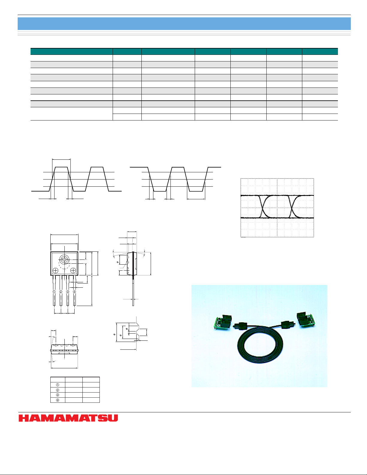
■ Input optical waveform definition
pw1
80 %
50 %
20 %
tr=2 ns tf=5 ns
■ Dimensional outline (unit: mm)
5.2 ± 0.3
(INCLUDING BURR)
5.0
10˚
4.5 ± 0.3
(INCLUDING BURR)
0.5
0.4
1.27
1.27 1.27
(SPECIFIED AT THE LEAD ROOT)
(0.9)
10˚
(0.9)
1.4
4.3
(2.15)
(1.5)
5.7 ± 0.4
■ Output optical waveform definition
1.8 V
1.5 V
1.2 V
tr tf
1.77
0.97
0.69
10˚
1.8
(0.9)
1.8
A
0.25
0.2
1.24
Surface B
0.25
4.3
0.66
■ S7141-10 output waveform example
(Input light is referenced by drive circuit
on front page)
(Ta=25 °C, Pi= -16 dBm, Vcc=5.0 V)
pw
∆T = pw1 - pw
KPICC0023EBKPICC0022EA
5 ns/div.
KPICC0068EA
■ An evaluation kit M7647 consisting of L7140-10,
S7141-10 and POF is also available.
10˚
5.0
L7140-10PIN No. S7141-10
CATHODE
CATHODE
ANODE
CATHODE
GND
OUT
GND
Vcc
Detail of part A
Lens tip does not project over surface B.
Tolerance unless otherwise
noted: ±0.1, ±2˚
Shaded area indicates burr.
Values in parentheses indicate
reference value.
Information furnished by HAMAMATSU is believed to be reliable. However, no responsibility is assumed for possible inaccuracies or omissions.
Specifications are subject to change without notice. No patent rights are granted to any of the circuits described herein. ©2002 Hamamatsu Photonics K.K.
KPICA0043EC
HAMAMATSU PHOTONICS K.K., Solid State Division
1126-1 Ichino-cho, Hamamatsu City, 435-8558 Japan, Telephone: (81) 053-434-3311, Fax: (81) 053-434-5184, http://www.hamamatsu.com
U.S.A.: Hamamatsu Corporation: 360 Foothill Road, P.O.Box 6910, Bridgewater, N.J. 08807-0910, U.S.A., Telephone: (1) 908-231-0960, Fax: (1) 908-231-1218
Germany: Hamamatsu Photonics Deutschland GmbH: Arzbergerstr. 10, D-82211 Herrsching am Ammersee, Germany, Telephone: (49) 08152-3750, Fax: (49) 08152-2658
France: Hamamatsu Photonics France S.A.R.L.: 8, Rue du Saule Trapu, Parc du Moulin de Massy, 91882 Massy Cedex, France, Telephone: 33-(1) 69 53 71 00, Fax: 33-(1) 69 53 71 10
United Kingdom: Hamamatsu Photonics UK Limited: 2 Howard Court, 10 Tewin Road, Welwyn Garden City, Her tfordshire AL7 1BW, United Kingdom, Telephone: (44) 1707-294888, Fax: (44) 1707-325777
North Europe: Hamamatsu Photonics Norden AB: Smidesvägen 12, SE-171 41 Solna, Sweden, Telephone: (46) 8-509-031-00, Fax: (46) 8-509-031-01
Italy: Hamamatsu Photonics Italia S.R.L.: Strada della Moia, 1/E, 20020 Arese, (Milano), Italy, Telephone: (39) 02-935-81-733, Fax: (39) 02-935-81-741
Cat. No. KPIC1039E04
Aug. 2002 DN
 Loading...