HAMAMATSU L7055-04 Datasheet

HIGH-POWER
■FEATURES
●High output power (φep≦20W)
●High speed rise time (tr=0.5 ns typ.)
■APPLICATIONS
●Laser rader
●Range finder
●Excitation light source
●Optical trigger
●Security barrier
INFRARED PULSED LASER DIODE
L7055-04
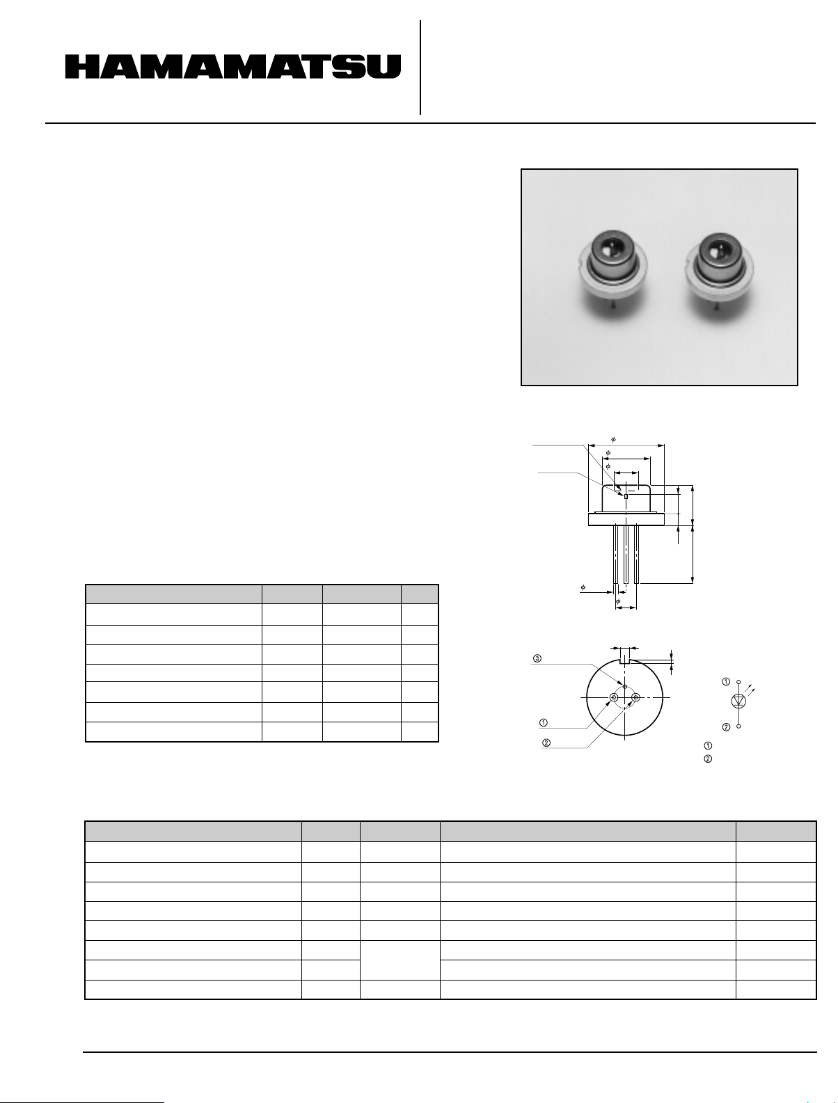
Figure 1: Dimensional Outline (Unit: mm)
+0
Glass Window
LD Chip
9.0
5.7
2.8
-0.1
± 0.2
± 0.3
■ABSOLUTE MAXIMUM RATINGS
Parameter
Pulsed Foward Current
Reverse Voltage
Pulsed Radiant Output Power
Pulse Duration (FWHM)
Duty Ratio
Operating Temperature
Storage Temperature
Symbol
FP
I
VR
φep
tw
DR
op
T
Tstg
Value
30
2
40
100
0.075
-30 to +85
-40 to +125
Unit
A
V
W
ns
%
℃
℃
NC (Case)
Anode
Cathode
■ELECTRICAL AND OPTICAL CHARACTERISTICS (Ta=25℃)
Parameter
Pulsed Radiant Power
Peak Emission Wavelength
Spectral Radiation Half Bandwidth
Forward Voltage
Rise Time
Beam Spread Angle : Parallel
: Vertical
Lasing Threshold Current
Note: General operating conditionφep≦20 W, tw≦50 ns, Repetition frequency≦8 kHz
Symbol
φ
λp
Δλ
V
tr
θ//
θ⊥
Ith
ep
F
Condition
FP=20A
I
I
FP=20A
FWHM
FP=20A
I
Min.
20
-
-
-
-
6
29
-
0.45
Typ.
-
870
4
6
0.5
8
32
1
2.54
Side View
1.0
Bottom View
2.41.5
7.0 ± 0.5 5.1 ± 0.5
0.4
Max.
-
-
-
-
-
10
35
-
(Pin Connection)
Anode
Cathode
Unit
W
nm
nm
V
ns
degree
degree
A
Information furnished by HAMAMATSU is believed to be reliable. However, no responsibility is assumed for possible inaccuracies or omissions.
Specifications are subject to change without notice. No patent rights are granted to any of the circuits described herein. 1998 Hamamatsu Photonics K.K.
C
○

HIGH-POWER INFRARED PULSED LASER DIODE L7055-04
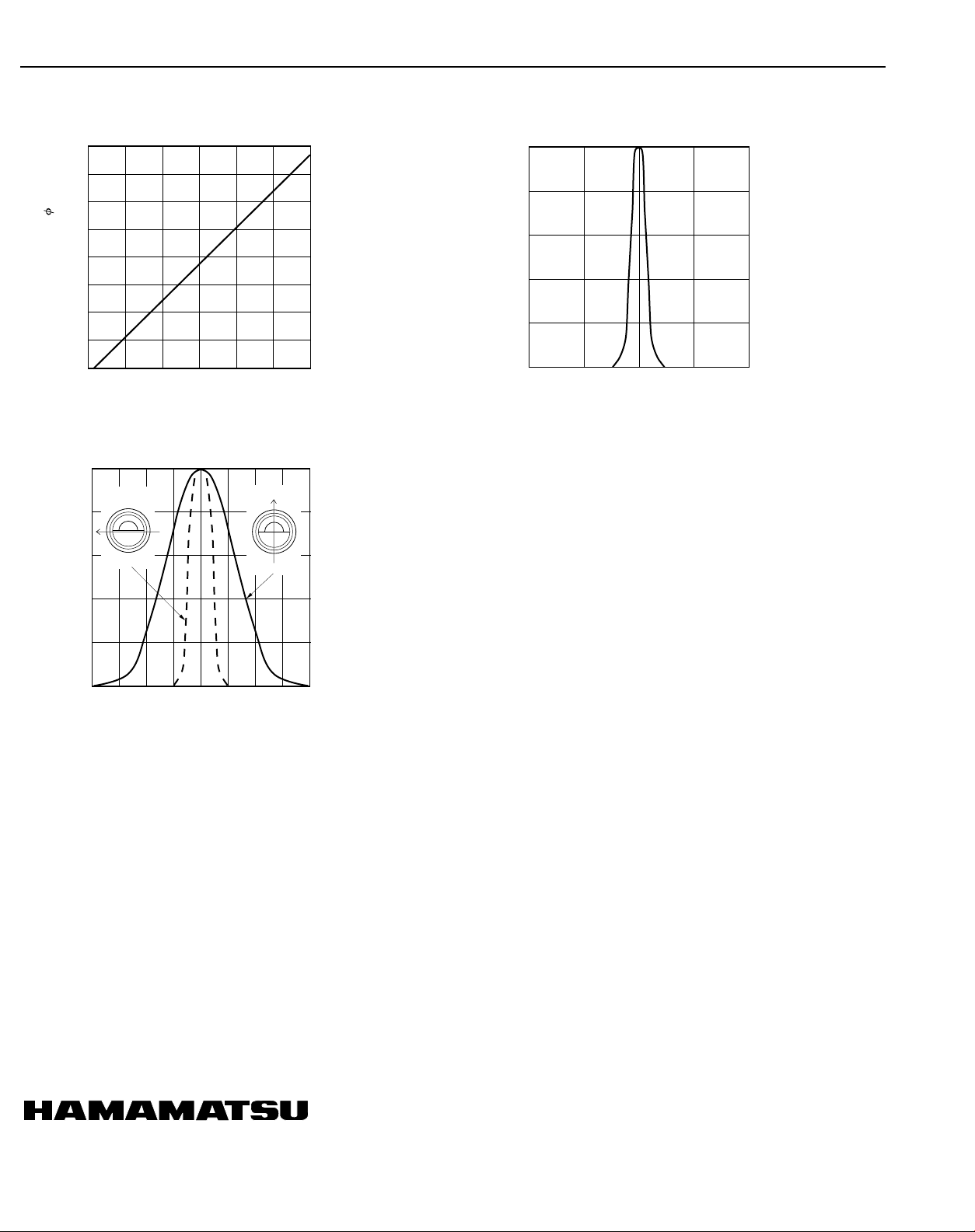
Figure 2: Typical Radiant Power vs.
Pulsed Forward Current
40
30
(Ta=25℃)
20
10
PULSED RADIANT POWER ep (W)
0
0102030
PULSED FORWARD CURRENT IFP (A)
Figure 4: Typical Directivity
FP=20 A, Ta=25℃)
100
Parallel
Direction
80
(I
Vertical Direction
Figure 3: Typical Emission Spectrum
100
80
60
40
20
RELATIVE RADIANT POWER (%)
0
870 890 910830 850
WAVELENGTH (nm)
(Ta=25℃)
60
Top View
40
20
RELATIVE RADIANT POWER (%)
0
Top View
3040 20 10 0 10 20 30 40
ANGLE (degree)
Top View
Top View
Handling Precautions for L7055-04
1. Precautions for handling
The LD (laser diode) may be damaged or its performance may deteriorate
due to such factors as electrostatic discharge from the human body, surge
voltages from measurement equipment, leakage voltages from soldering
irons, and packing materials. As a countermeasure against static electricity,
the device, operator, work place and measuring jigs must all be set at the
same electric potential. In using LD, observe the following precautions:
・To protect the device from static electricity charges which accumulate on
the operator or the operator’s clothes, use a wrist strap etc. to ground the
operator’s body via a high impedance resistor (1MΩ).
・A semiconductive sheet should be laid on both the work table and the
floor in the work area. When soldering, use an electrically grounded soldering iron with an isolation resistance of more than 10MΩ.
・For containers for transportation and packing, use of antistatic material
(material that minimizes the generation of static change when rubbed
against or separated from itself or other similar materials).
2. Precautions for mounting
(1)Lead forming
To form the leads, hold the base of the leads securely and bend them so
that no force is applied to the package. Lead forming should be done before soldering.
(2)Cutting off the leads
If leads are out when still at a high temperature, this may cause an electrical discontinuity. Always cut off the leads when they are at room temperature. Never cut off the leads immediately after they are soldered.
(3)Soldering
Using a low-temperature melting solder (below 200℃), solder the leads
at the temperature and dwell time specified as follows.
Maximum Soldering Temperature: 230℃
Maximum Soldering Time: 5 seconds (1 second for devices having a
lead length less than 2mm)
If these conditions cannot be met, it is recommended that some form of
heat sink be used at the base of the lead so that the solder heat is not
conducted to the package. Also be careful not to apply excessive force to
the leads during soldering.
Soldering at excessive temperatures and dwell times may cause the
roots of the leads to crack, resulting in performance deterioration. This
sometimes leads to wiring breakage. If the leads are soldered while external force is applied to the device, the residual force tends to degrade device performance. Care should also be taken not to apply force to the
leads during soldering.
In addition, when soldering an LD. use a soldering iron with its metallic
parts grounded to prevent damage to the device from static discharge.
Do not use any flux which is highly acidic. alkaline or inorganic because
it may cause the component leads to erode.
Use a rosin flux.
3.Protection against laser beams
The LD is classified into class 3B according to the laser product standards of the lEC825-1 (Radiation safety of laser products Part1: Equipment classification, requirements and user’s guide). The operator must
avoid eye or skin exposure to the laser beam. When viewing the laser
beam, be sure to wear safety goggles that block infrared radiation.
http://www.hamamatsu.com
HAMAMATSU PHOTONICS K.K., International Sales Division
325-6, Sunayama-cho, Hamamatsu City, 430-8587, Japan, Telephone: (81)53-452-2141, Fax: (81)53-456-7889
U.S.A.: Hamamatsu Corporation:360 Foothill Road, P.O. BOX 6910, Bridgewater, N.J. 08807-0910, U.S.A.Telephone: (1)908-231-0960, Fax: (1)908-231-1218 E-mail: usa@hamamatsu.com
Germany: Hamamatsu Photonics Deutschland GmbH: Arzbergerstr. 10, D-82211 Herrsching am Ammersee, Germany, Telephone: (49)8152-375-0, Fax: (49)8152-2658, E-mail: info@hamamatsu.de
France: Hamamatsu Photonics France S.A.R.L.: 8, Rue du Saule Trapu, Parc du Moulin de Massy, 91882 Massy Cedex, France, Telephone: 33(1) 69 53 71 00, Fax: 33(1) 69 53 71 10, E-mail: france@hamamatsu.com
United Kingdom: Hamamatsu Photonics UK Limited: 2 Howard Court, 10 Tewin Road, Welwyn Garden City, Hertfordshire AL7 1BW, United Kingdom, Telephone: (44)1707-294888, Fax: (44)1707-325777, E-mail: info@hamamatsu.co.uk
North Europe: Hamamatsu Photonics Norden AB: Smidesv gen 12, SE-171-41 Solna, Sweden, Telephone: (46)8-509-031-00, Fax: (46)8-509-031-01, E-mail: info@hamamatsu.se
Italy: Hamamatsu Photonics Italia S.R.L.: Strada della Moia, 1/E, 20020 Arese, (Milano), Italy, Telephone: (39)02-935 81 733, Fax: (39)02-935 81 741, E-mail: info@hamamatsu.it
Cat. No. LLD1004E02
Jul. 1999 T
Printed in Japan (1,000)
 Loading...