

HAMAMATSU L4100 Datasheet
LED
Infrared LED
L4100
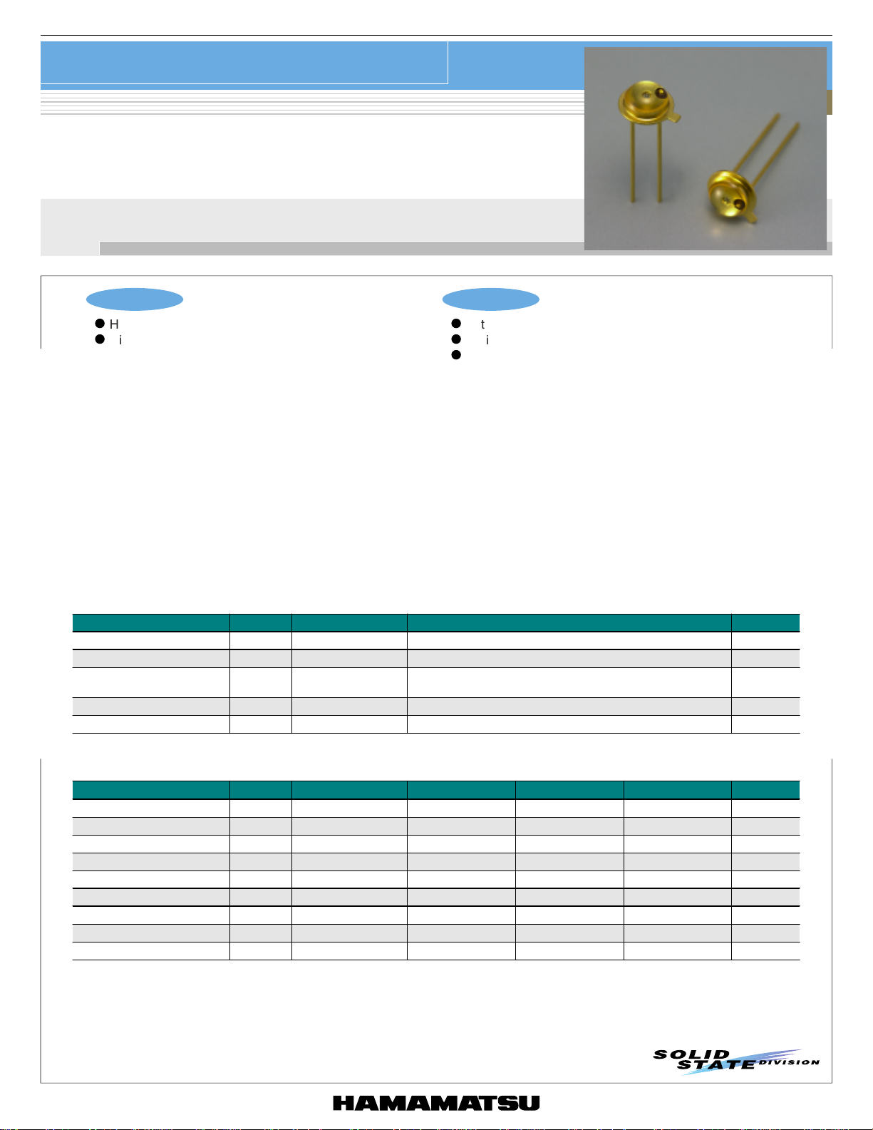
Resin-potted metal package LED
Features
l
High reliability
l
High output power
■
Absolute maximum ratings (Ta=25 °C)
Parameter Symbol Condition Value Unit
Forward current I
Reverse voltage V
Pulse forward current I
Operating temperature Topr -30 to +85
Storage temperature Tstg -40 to +100 *
* Guaranteed to resist temperature cycle test of up to 5 cycles
F
R
Pulse width=10 µs
FP
Duty ratio=1 %
Applications
l
Auto focus
l
Optical switches
l
Auto control equipment
70 mA
5 V
0.8 A
C
°
C
°
■
Electrical and optical characteristics (Ta=25 °C)
Parameter Symbol Condition Min. Typ. Max. Unit
Peak emission wavelength
Spectral half width
Forward voltage V
Pulse forward voltage V
Reverse current I
Radiant flux
Radiant illuminance P
Rise time tr IF=50 mA - 0.45 0.7 µs
Fall time tf IF=50 mA - 0.45 0.7 µs
IF=50 mA 870 890 920 nm
p
λ
IF=50 mA - 50 - nm
∆λ
IF=50 mA - 1.45 1.60 V
F
FPIF
R
φ
=0.8 A - 3 3.7 V
VR=5 V - - 5 µA
IF=50 mA 12 14 - mW
e
IF=50 mA - 1.3 - mW/cm
E
2
Infrared LED
FORWARD VOLTAGE (V)
(Typ. Ta=25 ˚C, tw=100 µs, 0.1 %)
FORWARD CURRENT (mA)
1.0 1.5
1
1000
100
10
2.0 2.5 3.0 3.5
-40 -20 0 20 40 60 80 100
1.30
1.40
1.35
1.45
1.50
1.55
1.60
AMBIENT TEMPERATURE (˚C)
FORWARD VOLTAGE (V)
(Typ. IF=50 mA)
L4100
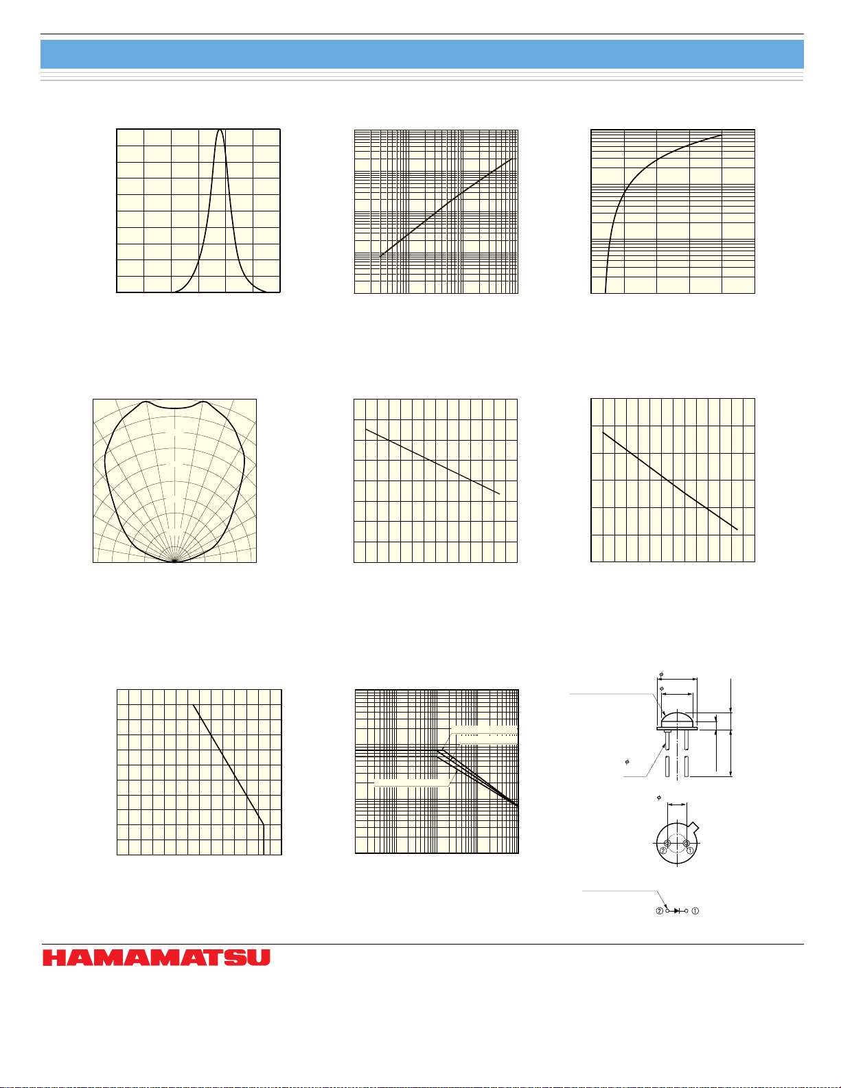
■ Emission spectrum ■ Radiant flux vs. forward current
100
80
60
40
20
RELATIVE RADIANT OUTPUT (%)
0
700 800 900 1000
WAVELENGTH (nm)
■ Directivity
20˚ 10˚ 0˚ 10˚ 20˚
30˚
40˚
50˚
60˚
70˚
80˚
90˚
RELATIVE RADIANT OUTPUT (%)
100%
(Typ. Ta=25 ˚C, IF=50 mA)
80 %
60 %
40 %
20 %
(Typ. Ta=25 ˚C)
30˚
40˚
50˚
60˚
70˚
80˚
90˚
1000
100
10
RADIANT FLUX (mW)
1
0.1
KLEDB0117EB
■ Radiant output vs. ambient
temperature
+3
+2
+1
0
-1
-2
-3
-4
RELATIVE RADIANT OUTPUT (dB)
-5
-40 -20 0 20 40 60 80 100
KLEDB0179EA
(Typ. Ta=25 ˚C, tw=100 µs, 0.1 %)
101 100 1000
FORWARD CURRENT (mA)
(Typ. IF=50 mA)
AMBIENT TEMPERATURE (˚C)
■ Forward current vs. forward voltage
KLEDB0177EA
■ Forward voltage vs. ambient
temperature
KLEDB0145EA
KLEDB0178EA
KLEDB0180EA
■ Allowable forward current vs.
ambient temperature
(Typ.)
100
80
60
40
20
0
RELATIVE ALLOWABLE FORWARD CURRENT (%)
-40 -20 0 20
AMBIENT TEMPERATURE (˚C)
HAMAMATSU PHOTONICS K.K., Solid State Division
1126-1 Ichino-cho, Hamamatsu City, 435-8558 Japan, Telephone: (81) 053-434-3311, Fax: (81) 053-434-5184, http://www.hamamatsu.com
U.S.A.: Hamamatsu Corporation: 360 Foothill Road, P.O.Box 6910, Bridgewater, N.J. 08807-0910, U.S.A., Telephone: (1) 908-231-0960, Fax: (1) 908-231-1218
Germany: Hamamatsu Photonics Deutschland GmbH: Arzbergerstr. 10, D-82211 Herrsching am Ammersee, Germany, Telephone: (49) 08152-3750, Fax: (49) 08152-2658
France: Hamamatsu Photonics France S.A.R.L.: 8, Rue du Saule Trapu, Parc du Moulin de Massy, 91882 Massy Cedex, France, Telephone: 33-(1) 69 53 71 00, Fax: 33-(1) 69 53 71 10
United Kingdom: Hamamatsu Photonics UK Limited: 2 Howard Court, 10 Tewin Road, Welwyn Garden City, Hertfordshire AL7 1BW, United Kingdom, Telephone: (44) 1707-294888, Fax: (44) 1707-325777
North Europe: Hamamatsu Photonics Norden AB: Smidesvägen 12, SE-171 41 Solna, Sweden, Telephone: (46) 8-509-031-00, Fax: (46) 8-509-031-01
Italy: Hamamatsu Photonics Italia S.R.L.: Strada della Moia, 1/E, 20020 Arese, (Milano), Italy, Telephone: (39) 02-935-81-733, Fax: (39) 02-935-81-741
40 60 80 100
■ Allowable forward current vs.
duty ratio
10
1
PULSE WIDTH=100 µs
0.1
ALLOWABLE FORWARD CURRENT (A)
0.01
0.01 0.1 1 10 100
KLEDB0027EB
Information furnished by HAMAMATSU is believed to be reliable. However, no responsibility is assumed for possible inaccuracies or omissions.
Specifications are subject to change without notice. No patent rights are granted to any of the circuits described herein. ©2001 Hamamatsu Photonics K.K.
DUTY RATIO (%)
(Typ. Ta=25 ˚C)
PULSE WIDTH=1 µs
PULSE WIDTH=10 µs
■ Dimensional outline (unit: mm)
CLEAR EPOXY RESIN
0.45
LEAD
KLEDB0037EB
COMMON TO CASE
5.4 ± 0.1
4.2 ± 0.1
2.54 ± 0.2
2.3 ± 0.3
13.5
1.12 ± 0.1
KLEDA0009ED
Cat. No. KLED1026E01
Apr. 2001 DN
 Loading...