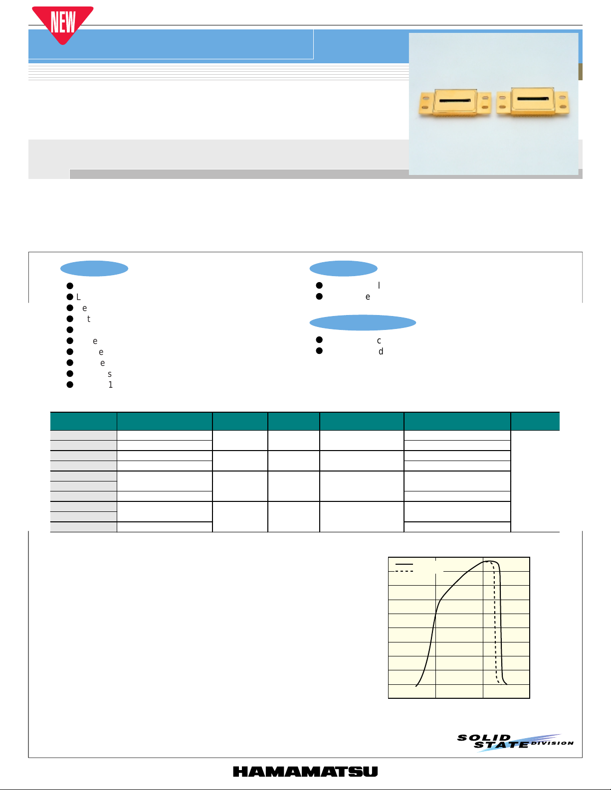
HAMAMATSU G9204-512S, G9204-512R, G9204-512D, G9203-256S, G9203-256R Datasheet
...
IMAGE SENSOR
0.5
1.0
1.5
2.0
0
0.5
1.0
WAVELENGTH (µm)
PHOTO SENSITIVITY (A/W)
(Typ.)
T=25
˚C
T= -10
˚C
InGaAs linear image sensor
G9201 to G9204 series
Image sensor for DWDM wavelength monitor
G9201 to G9204 series InGaAs linear image sensors are specifically designed as detectors for monitoring WDM in optical communications. These
linear image sensors consist of an InGaAs photodiode array with each pixel connected to a charge amplifier array comprised of CMOS transistors,
a CDS circuit, an offset compensation circuit, a shift register and a timing generator. These sensors deliver high sensitivity and stable operation in
the near infrared spectral range. The package is hermetically sealed for high reliability and the window has an anti-reflective coating for efficient
light detection.
Signal processing circuits on the CMOS chip allow selecting a feedback capacitance (Cf) of 10 pF or 0.5 pF by supplying an external voltage. The
image sensor operates over a wide dynamic range when Cf=10 pF and delivers high gain when Cf=0.5 pF.
Features
l
Wide dynamic range
l
Low noise and low dark current
l
Selectable gain
l
Anti-saturation circuit
l
CDS circuit *
l
Offset compensation circuit
l
Simple operation (by built-in timing generator) *
l
High resolution: 25 µm pitch (512 ch)
l
Low cross-talk
l
256 ch: 1 video line
512 ch: 2 video lines
■ Selection guide
Type No. Coo ling
G9201-256R
G9201-256S
G9202-512R
G9202-512S
G9203-256D *
G9203-256R
G9203-256S
G9204-512D *
G9204-512R
G9204-512S
*1: CDS (Correlated Double Sampling) circuit
A major source of noise in charge amplifiers is the reset noise generated when the integration capacitance is reset. A CDS circuit greatly
reduces this reset noise by holding the signal immediately after reset to find the noise differential.
*2: Timing generator
Different signal timings must be properly set in order to operate a
shift register. In conventional image sensor operation, external PLDs
(Programmable Logic Devices) are used to input the required timing
signals. However, G9201 to G9204 series image sensors internally
generate all timing signals on the CMOS chip just by supplying CLK
and RESET pulses. This makes it simple to set the timings.
*3: G9203-256D and G9204-512D are not available for C7557.
*4: For G9203-256D and G9204-512D specifications, see the separate
data sheets available from Hamamatsu.
1
Non-cooled 0.9 to 1.7 (25 °C )
One-stage TE-cooled
Non-cooled 0.9 to 1.7 (25 °C )
One-stage TE-cooled
4
4
Non-cooled 0.9 to 1.7 (25 °C )
One-stage TE-cooled
Non-cooled 0.9 to 1.7 (25 °C )
One-stage TE-cooled
2
Number of
pixels
256 50 50 × 250
512 25 25 × 250
256 50 50 × 500
512 25 25 × 500
Pixel pitch
(µm )
Applications
l
DWDM wavelength monitor
l
Optical spectrum analyzer
Accessories (Optional)
l
InGaAs multichannel detector head C8061-01, C8062-01 *
l
Multichannel detector head controller C7557 *
Pixel size
[µm (H) × µm (V )]
Spectral response range
(µm )
0.9 to 1.67 (-10 °C)
0.9 to 1.67 (-10 °C)
0.9 to 1.67 (-10 °C)
0.9 to 1.67 (-10 °C)
■ Spectral response
3
Defective
pixel
KMIRB0011EA
3
0
1

InGaAs linear image sensor
G9201 to G9204 series
■ Absolute maximum ratings
Parameter Symbol Value Unit
Clock pulse voltage V
Operating temperature *
Storage temperature *
1
1
Topr -40 to +70 °C
Tstg -40 to +85 °C
φ
5.5 V
*1: Non condensation
■ Electrical characteristics (Ta=25 °C, Vφ=5 V )
Parameter Symbol Min. Typ . Max. Unit
Supply voltage
Ground Vss - 0 - V
Element bias INP 4.4 4.5 4.6 V
Clock frequency f 0.01 - 4 MHz
Clock pulse voltage
high 4.5 V
low
Clock pulse rise/fall times
Clock pulse width tpw
Reset pulse voltage
high 4.5 V
low
Reset pulse rise/fall times
Reset pulse width tpw (RES) 6000 - - ns
Video output voltage
high V
low V
Data rate f
Vdd 4.9 5.0 5.1
Vref - 1.26 -
V
φ
tr
φ
tf
φ
φ
V (RES)
tr (RES)
tf (RES)
H
L
V
000.4V
0 20 100 ns
200 - - ns
0 0 0.4 V
0 20 100 ns
- 4.4 INP
-1.26-
- f/8 - Hz
φ
φ
5.5 V
5.5 V
V
V
■ Electrical and optical characteristics
General ratings (T=25 °C)
Parameter Symbol Condition Min. Typ . Max. Unit
Peak sensitivity wavelength
Saturation charge
*2
p - 1.55 - µm
λ
Qsat Vp=5 V - 30 - pC
Standard deviation
RMS noise voltage (readout noise) N
Number of
- 180 300 µVrms
integration: 50
Photo response non-uniformity
*3
PRNU
Integration time:
10 msec
--±5%
Saturation voltage Vsat 3.0 3.2 - V
*2: Vφ=5 V, Cf=10 pF
*3: 50 % of saturation, 10 ms integration time, after dark output subtraction, excluding first and last pixels.
Dark current characteristics (T=25 °C)
Parameter Symbol Min. Typ. Max. Unit
G9201 series - 2 10
G9202 series - 1 5
G9203 series - 4 20
G9204 series
D
I
- 1 5
pA
2
 Loading...