

HAMAMATSU G8921-01 Datasheet
PHOTODIODE
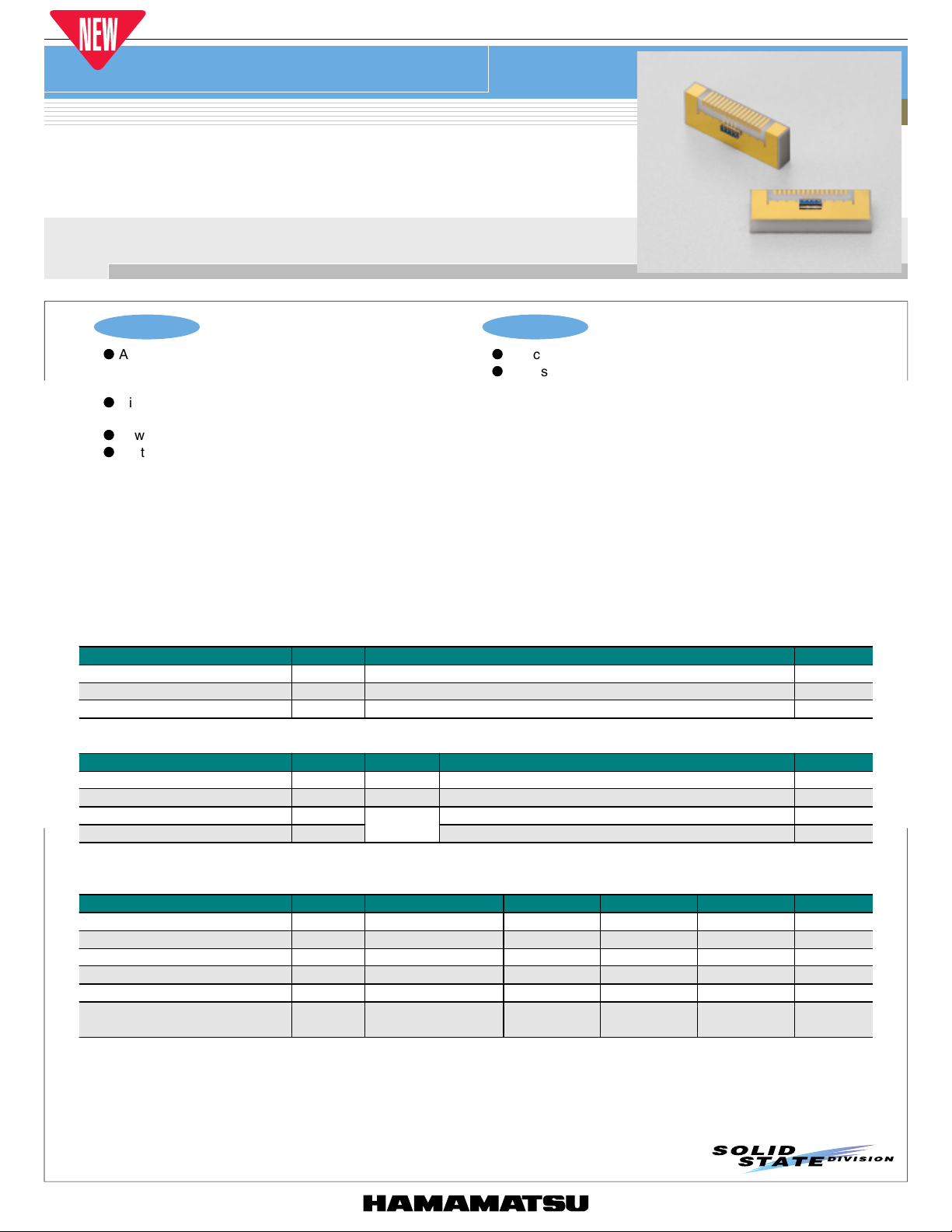
GaAs PIN photodiode array
G8921-01
Photodiode array for data communication
Features
l
Active area: φ0.06 mm
Element pitch: 250 µm
4-element array
l
High-speed response: 10 Gbps [(2.5 Gbps per channel) ×4]
at low bias voltage (V
l
Low dark current, low capacitance
l
Up to 16 elements available as option
R=2 V)
Applications
l
Optical fiber communications
l
High-speed data link
■ General ratings
Parameter Symbol Value Unit
Active area - f0.06 mm
Element pitch - 250 µm
Number of elements - 4 ch
■ Absolute maximum ratings
Parameter Symbol Remark Value Unit
Reverse voltage VR Max
Reverse current IR Max. 0.5 mA
Operating temperature Topr -40 to +85 °C
Storage temperature Ts tg
* In N2 environment or in vacuum
.
*
30 V
-55 to +125 °C
■ Electrical and optical characteristics (Unless other wise, Ta=25 °C, per 1 element)
Parameter Symbol Condition Min. Typ . Max. Unit
Spectral response range l - 470 to 870 - nm
Peak sensitivity wavelength
Photo sensitivity S l=850 nm 0.45 0.5 - A/W
Dark current I
Terminal capacitance Ct VR=2 V, f=1 MHz - 0.35 0.5 pF
Cut-off frequency fc
lp
VR=5 V - 2 50 pA
D
l=850 nm, VR
RL=50 W, -3 dB
=2 V,
- 850 - nm
2 - - GHz
1
GaAs PIN photodiode array
G8921-01
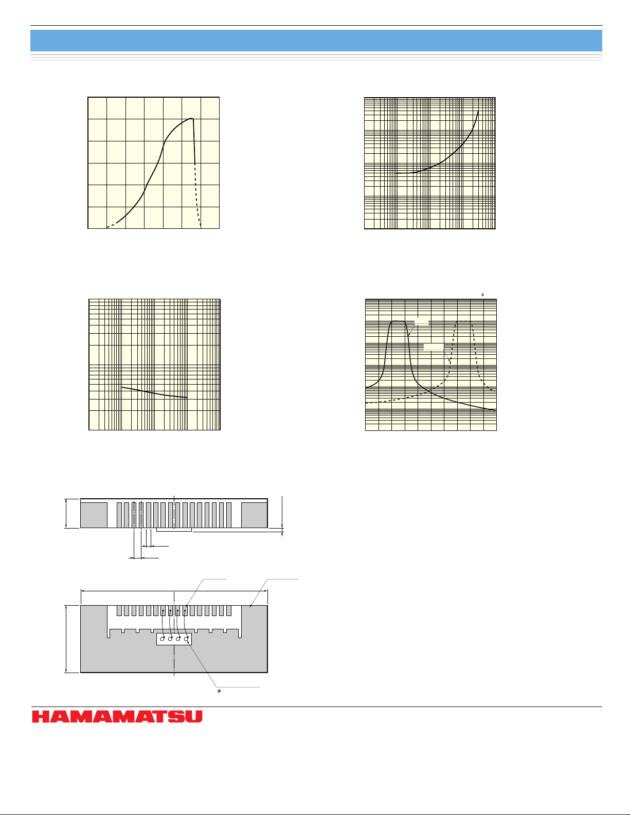
■ Spectral response
0.6
0.5
0.4
0.3
0.2
PHOTO SENSITIVITY (A/W)
0.1
0
300 500 600 700 800 900 1000400
WAVELENGTH (nm)
(Typ. Ta=25 ˚C)
KGPDB0048EA
■ Terminal capacitance vs. reverse voltage
10 pF
1 pF
(Typ. Ta=25 ˚C)
■ Dark current vs. reverse voltage
10.10.01
(Typ. Ta=25 ˚C)
10 100
100 pA
10 pA
1 pA
DARK CURRENT
100 fA
10 fA
REVERSE VOLTAGE (V)
■ Cross-talk characteristic
(Typ. Ta=25 ˚C, λ=830 nm, step: 5 µm, Pin=20 nW, spot light size: 10 µm)
1000
100
10
1
n ch
n+1 ch
KGPDB0049EA
TERMINAL CAPACITANCE
100 fF
10.10.01
10 100
REVERSE VOLTAGE (V)
■ Dimensional outline (unit: mm)
0.15
0.25
6.4
2.30 1.0
KGPDB0050EA
ANODE
ACTIVE AREA
0.06 × 4 ch
0.2 ± 0.05
CATHODE
KGPDA0017EA
0.1
RELATIVE SENSITIVITY (%)
0.01
0.001
0 100 200 300 400 500
POSITION (µm)
KGPDB0051EA
Information furnished by HAMAMATSU is believed to be reliable. However, no responsibility is assumed for possible inaccuracies or omissions.
Specifications are subject to change without notice. No patent rights are granted to any of the circuits described herein. ©2002 Hamamatsu Photonics K.K.
HAMAMATSU PHOTONICS K.K., Solid State Division
1126-1 Ichino-cho, Hamamatsu City, 435-8558 Japan, Telephone: (81) 053-434-3311, Fax: (81) 053-434-5184, http://www.hamamatsu.com
U.S.A.: Hamamatsu Corporation: 360 Foothill Road, P.O.Box 6910, Bridgewater, N.J. 08807-0910, U.S.A., Telephone: (1) 908-231-0960, Fax: (1) 908-231-1218
Germany: Hamamatsu Photonics Deutschland GmbH: Arzbergerstr. 10, D-82211 Herrsching am Ammersee, Germany, Telephone: (49) 08152-3750, Fax: (49) 08152-2658
France: Hamamatsu Photonics France S.A.R.L.: 8, Rue du Saule Trapu, Parc du Moulin de Massy, 91882 Massy Cedex, France, Telephone: 33-(1) 69 53 71 00, Fax: 33-(1) 69 53 71 10
United Kingdom: Hamamatsu Photonics UK Limited: 2 Howard Court, 10 Tewin Road, Welwyn Garden City, Her tfordshire AL7 1BW, United Kingdom, Telephone: (44) 1707-294888, Fax: (44) 1707-325777
North Europe: Hamamatsu Photonics Norden AB: Smidesvägen 12, SE-171 41 Solna, Sweden, Telephone: (46) 8-509-031-00, Fax: (46) 8-509-031-01
Italy: Hamamatsu Photonics Italia S.R.L.: Strada della Moia, 1/E, 20020 Arese, (Milano), Italy, Telephone: (39) 02-935-81-733, Fax: (39) 02-935-81-741
2
Cat. No. KGPD1009E02
Jul. 2002 DN
 Loading...