HAMAMATSU C9004 Datasheet

MODULE
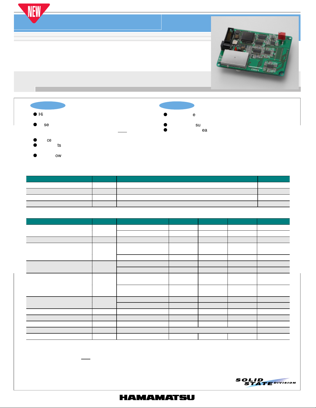
Driver circuit for Si photodiode array
C9004
Driver circuit for 16-element photodiode array
Features Applications
l
High precision and high-speed measurement by
simultaneous 16-channel readout
l
Assembled with pulse generator (8-step adjustable
oscillatory frequency)
CLK, START, A/D conversion Trig and EOS pulse output
lChoice of gain (conversion impedance): 1 × 10⁶ or 1 × 10⁷ (V/A)
l
Hamamatsu S4111-16 series, S5668 series and S8592
photodiode arrays are directly mountable on board.
l
Single power supply operation: +12 V
■ Absolute maximum ratings
Parameter Symbol Value Unit
Supply voltage Vcc Max. +18 V
Input current Iin Max. +6.7 × 10
Operating temperature Topr 0 to +50 °C
Storage temperature Tstg -20 to +80
l
Performance evaluation of Hamamatsu S4111-16 series,
S5668 series and S8592 photodiode arrays
l
Position measurement
l
Displacement measurement
-5
A
°C
■ Electrical and optical characteristics (Ta=25 °C)
Parameter Symbol Condition Min. Typ. Max. Unit
Input current range Iin
Conversion impedance *
1
Tz 1 × 10
Tz=1 × 10
Tz=1 × 10
Tz=1 × 10
Output offset voltage Vos
(set up prior to shipping)
Tz=1 × 10
Output amplitude voltage Vo
Tz=1 × 10⁶, RL=1 kW 0 - +10 V
Tz=1 × 10⁷, RL=1 kW 0 - +10 V
Tz=1 × 10
Output noise voltage
e
np-p
(full bandwidth)
Tz=1 × 10
(full bandwidth)
Rise time tr
Capacitive load C
Oscillatory frequency (OUT) *
Start pulse width (OUT) *
Output format *
4
3
3
CLK 1.5625 - 200 kHz
Tz=1 × 10⁶, RL=1 kW - 5.6 - µs
Tz=1 × 10⁷, RL=1 kW - 5.6 - µs
L
- 5 - 640 µs
- TTL Current consumption Icc - 200 250 mA
*1: Conversion impedance can be changed with the switch on the circuit board.
*2: The variable resistor V
on the circuit board must be used for making offset adjustments.
R
*3: Adjustable in 8 steps by using the BCD rotary switch on the circuit board.
*4: CLK, START, Trig and EOS pulse output format.
6
7
6
7 *2
6
7
- - 1 × 10
- - 1 × 10
6
- 1 × 10
-5
-6
7
A
A
V/A
-0.025- V
-0.25- V
-5-mVp-p
-10-mVp-p
- - 100 pF
PRELIMINARY DATA
Aug. 2002
1

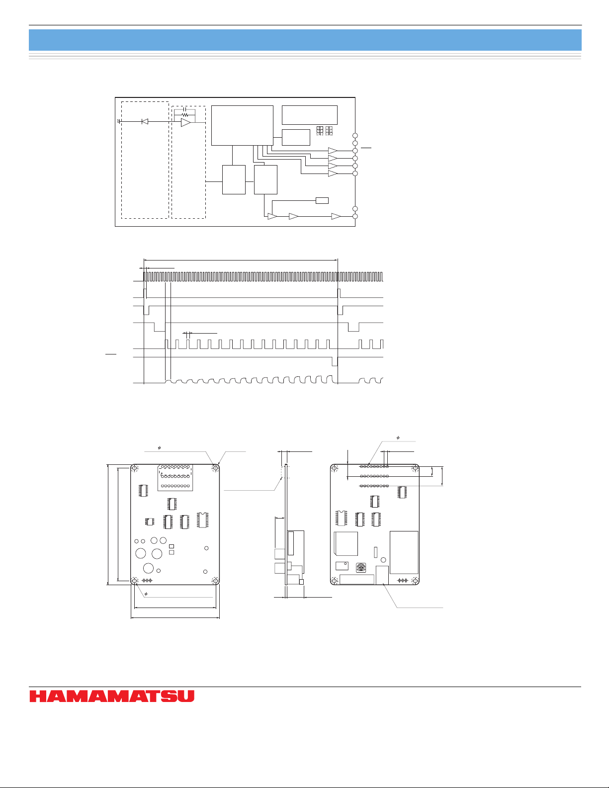
■ Block diagram
16-ELEMENT
PHOTODIODE
········
S4111-16
S5668
S8592
CURRENT-VOLTAGE
CONVERSION AMP
5
5 × 10
········
× 16 ch
TIMING GENERATOR
S/H MUX
Driver circuit for Si photodiode array
DC-DC CONVERTER
OSCILLATOR
×2 or ×20
JP
SW
BUFFER
+12 V
GND
EOS
Tr ig
START
CLK
GND
Vout
KACCC0181EA
C9004
■ Timing chart
5 µs MIN.
CLK
START
(S/H)
(Reset)
Trig.
EOS
Signal out
■ Dimensional outline (unit: mm)
Photodiode array mount side
(4 ×) 3.2 (THRU HOLE)
89.0
95.0
5 µs MIN.
360 µs MIN.
(4 ×) R3
PHOTODIODE ARRAY
MOUNT POSITION
Back side
4.5 MAX. P2.54 × 8
9.94
8.0
KACCC0182EA
(27 ×) 0.8TH
7.62
15.24
BCD SWITCH
CN
6 LAND PATTERN FOR GND
64.0
70.0
NOTE) Photodiode array sold separately
1.6
12.5 MAX.
DC JACK
FOR AC ADAPTER
KACCA0117EB
■ Accessories
· Dedicated AC adapter
· Flat cable (20 cm) with I/O connector receptacle
Information furnished by HAMAMATSU is believed to be reliable. However, no responsibility is assumed for possible inaccuracies or omissions.
HAMAMATSU PHOTONICS K.K., Solid State Division
1126-1 Ichino-cho, Hamamatsu City, 435-8558 Japan, Telephone: (81) 053-434-3311, Fax: (81) 053-434-5184, http://www.hamamatsu.com
U.S.A.: Hamamatsu Corporation: 360 Foothill Road, P.O.Box 6910, Bridgewater, N.J. 08807-0910, U.S.A., Telephone: (1) 908-231-0960, Fax: (1) 908-231-1218
Germany: Hamamatsu Photonics Deutschland GmbH: Arzbergerstr. 10, D-82211 Herrsching am Ammersee, Germany, Telephone: (49) 08152-3750, Fax: (49) 08152-2658
France: Hamamatsu Photonics France S.A.R.L.: 8, Rue du Saule Trapu, Parc du Moulin de Massy, 91882 Massy Cedex, France, Telephone: 33-(1) 69 53 71 00, Fax: 33-(1) 69 53 71 10
United Kingdom: Hamamatsu Photonics UK Limited: 2 Howard Court, 10 Tewin Road, Welwyn Garden City, Hertfordshire AL7 1BW, United Kingdom, Telephone: (44) 1707-294888, Fax: (44) 1707-325777
North Europe: Hamamatsu Photonics Norden AB: Smidesvägen 12, SE-171 41 Solna, Sweden, Telephone: (46) 8-509-031-00, Fax: (46) 8-509-031-01
Italy: Hamamatsu Photonics Italia S.R.L.: Strada della Moia, 1/E, 20020 Arese, (Milano), Italy, Telephone: (39) 02-935-81-733, Fax: (39) 02-935-81-741
Specifications are subject to change without notice. No patent rights are granted to any of the circuits described herein. ©2002 Hamamatsu Photonics K.K.
2
Cat. No. KACC1081E01
Aug. 2002 DN
 Loading...