HAMAMATSU C8892 Datasheet

IMAGE SENSOR
NMOS multichannel detector head
C8892
Integrated low-noise driver/amplifier circuit for NMOS linear image sensor
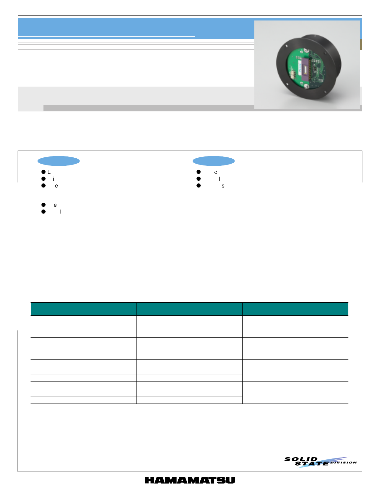
C8892 is multichannel detector head incorporating low-noise driver/amplifier circuit developed for Hamamatsu NMOS linear image sensors.
C8892 is designed especially for compactness, having an overall length as short as 40 mm or less.
In addition, C8892 is designed for ease of use. It is provided with circular flange for connection to monochrometer and adjustment mechanism for
optical alignment for NMOS linear image sensor. The flange is interchangeable, thus facilitating connection to various models of monochrometer.
The housing case also provides a shielding effect against external noise. As useful options, peripheral devices are available for driving C8892,
and for the output signal processing.
Features
l
Low noise
l
Wide dynamic range
l
Operatable with simple input signals
(Only a master start pulse, a master clock pulse,
±15 V are required.)
l
Interchangeable flange
l
Simple electrical and optical adjustments
■ Compatible NMOS linear image sensors
Type No. of
NMOS linear image sensor *
S3901-128Q, S8380-128Q 128
S3901-256Q/F, S8380-256Q 256
S3901-512Q/F, S8380-512Q 512
S3902-128Q 128
S3902-256Q/F 256
S3902-512Q/F 512
S3903-256Q 256
S3903-512Q/F 512
S3903-1024Q/F 1024
S3904-256Q, S8381-256Q 256
S3904-512Q/F, S8381-512Q 512
S3904-1024Q/F, S8381-1024Q 1024
*1: The suffix of type number indicates:
Q: quartz window, F: fiber optic window
1
Number of pixels
Applications
l
Multichannel spectrophotometry
l
Optical spectrum analysis
l
Time-resolved photometry
Active area per pixel
(pixel pitch × height)
50 µm × 2.5 mm
50 µm × 0.5 mm
25 µm × 0.5 mm
25 µm × 2.5 mm
1

NMOS multichannel detector head
C8892
■ Absolute maximum ratings
Parameter Symbol Value Unit
Supply voltage (analog) Va ±18 V
Operating temperature Topr 0 to 50 *
Storage temperature Tstg -10 to 60 *
2
2
*2: No condensation
■ Electrical characteristics (Ta=25 °C)
Parameter Symbol Min. Typ. Max. Unit
Supply voltage Analog Va ±14.5 ±15.0 ±15.5 V
Master start
pulse (φms)
Input
Voltage
Width
Rise/fall Time
Voltage
Master clock
pulse (φmc)
Frequency
*3
Width
Rise/fall time
Start pulse
(φst)
Voltage
Rise/fall time
Width
Voltage
Rise/fall time
Output
Clock pulse
(φ1, φ2)
*4
Clock pulse (φ1) width tpwφ1
Clock pulse (φ2) width tpwφ2
End of scan
pulse
Voltage
Rise/fall time treos, tfeos - - 100 ns
Width tpweos -
Trigger pulse
Voltage
Rise/fall time trtrig, tftrig - - 100 ns
*3: The operation of 50 % Typ. duty ratio is recommended.
*4: The outputs of start-pulse and clock-pulse are to be obtained from a front part where an image sensor is
installed. The outputs of end-of-scan and trigger-pulse are to be obtained from a back-side part where a
connector for input/output signal is fixed.
Vms (H) 2.0 5.0 -
Vms (L) 0 - 0.8
tpwφms 1/fφmc
trφms, tfφms
- - 500 ns
- - s
Vmc (H) 2.0 5.0 -
Vmc (L) 0 - 0.8
fφmc
tpwφmc
trφmc, tfφmc
- - 375 kHz
30 - - ns
- - 500 ns
Vst (H) 4.75 5.0 -
Vst (L) 0 - 0.4
trφst, tfφst
tpwφst
- - 100 ns
-
2/fφmc
V1, V2 (H) 4.75 5.0 -
V1, V2 (L) 0 - 0.4
trφ1, trφ2
tfφ1, tfφ2
- - 100 ns
-
-
3/fφmc
3/fφmc
Veos (H) 4.75 5.0 Veos (L) - - 0.4
3/fφmc
Vtrig (H) 4.0 5.0 Vtrig (L) 0 - 0.4
- s
- s
-s
- s
°C
°C
V
V
V
V
V
V
2
 Loading...