

HAMAMATSU C7942CA Datasheet
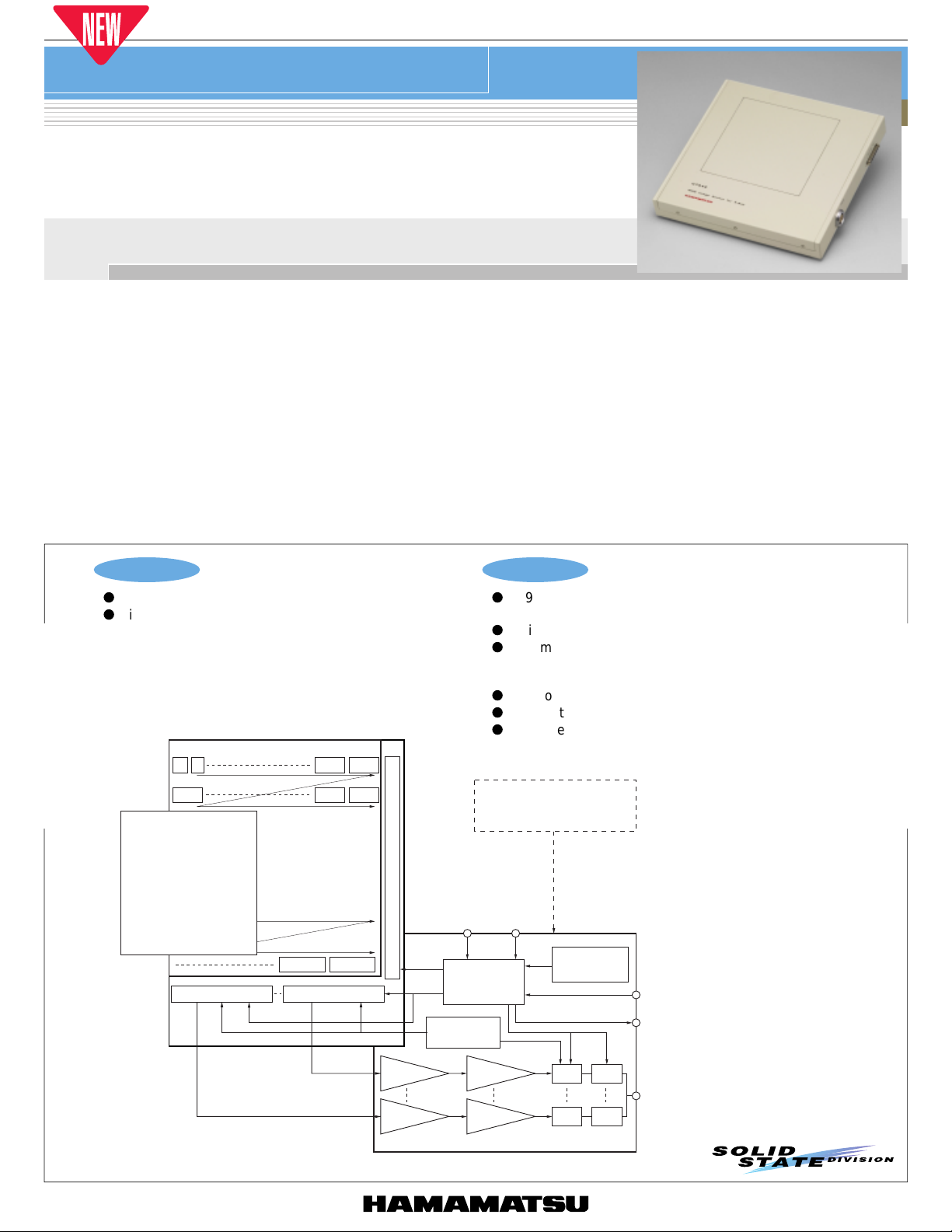
IMAGE SENSOR
Flat panel sensor
C7942CA, C7943CA
Acquire digital X-ray image in real time and 170 & 176 mm diagonal size
Hamamatsu C7942CA and C7943CA Flat Panel Sensors are digital X-ray image sensors newly developed as key devices for non-destructive
inspection, biomedical imaging, X-ray microscopy and other real-time X-ray imaging applications requiring high resolution and high image quality.
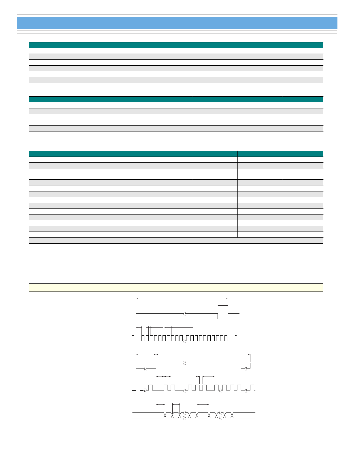
C7942CA and C7943CA consist of a sensor board and a control board, both assembled in a thin, flat and compact package. The sensor board
contains a CsI scintillator plate, a two-dimensional photodiode array with FET switches and a signal processing IC chip. The photodiode array has
a 2400 × 2400 (C7942CA) or 1248 × 1248 (C7943CA) pixel format with minimized blooming and is highly sensitive to bluish green light emitted
from the CsI scintillator. Each row of pixels is addressed in sequence by the vertical shift register connected to the gate line.
Light emission occurs when X-rays are absorbed in the CsI scintillator. This light emission enters directly into the two-dimensional photodiode
array where an electric charge is stored in each pixel according to the light intensity. This charge is then transferred to the corresponding data line
by applying a control signal to the vertical shift register.
The sensor board also has 8 charge sensitive amplifier arrays each having 300 channel (C7942CA) or 156 channel (C7943CA) amplifiers with a
horizontal shift register. These amplifiers with a total of 2400 channels (C7942CA) or 1248 channels (C7943CA) are connected to a CDS
(Correlated Double Sampling) circuit that senses the charge on each video line and sends it as the analog video signal from each amplifier array.
The control board converts the analog video signal into a 12-bit digital signal and outputs it to an external frame grabber from a 12-bit parallel port.
C7943CA delivers a frame rate of 30 frames per second using 4 × 4 binning and is ideal for high frame rate applications. On the other hand,
C7942CA is ideal for applications requiring high resolution because of its 50 µm pixel size. Massive digital image data can easily be monitored on
a display unit by using a frame grabber board and video memory installed in the PC. C7942CA and C7943CA will prove ideal tools for real-time Xray imaging and processing where easy-to-use, high-resolution X-ray digital image sensors are needed.
Applications
l
Non-destructive inspection
l
Digital X-ray photography
■ Block diagram (C7942CA)
PIXEL NUMBER
12
SCINTILLATOR
(120 mm × 120 mm)
AMP ARRAY No. 1
24002339
480047992401
PHOTODIODE
ARRAY
57600005759999
AMP ARRAY No. 8
SHIFT REGISTER
IntExt
TIMING
PULSE
GENERATOR
BIAS
GENERATER
Features
l
C7942CA: 2400 × 2400 pixels
C7943CA: 1248 × 1248 pixels
l
Digital output (12 bit)
l
Dynamic picture image
C7942CA: 9 frame/s (4 × 4 binning)
C7943CA: 30 frame/s (4 × 4 binning)
l
Low noise and wide dynamic range
l
Compact package
l
Easy use
EXTERNAL POWER SUPPLY
A. Vdd, D. Vdd V (±7.5)
(not attached)
IntExt
BINNING
(bin0, bin1)
OSCILLATOR
ExtTrg
Vsync
Hsync
Pclk
BUFFER
AMP
BUFFER
AMP
PROCESSING
AMP
PROCESSING
AMP
A/D
FIFO
A/D FIFO
VIDEO OUTPUT
(12 BIT DIGITAL)
KACCC0137EA
1
■
Vsync+
(RS-422)
Hsync+
(RS-422)
Hsync+
(RS-422)
Pclk+
(RS-422)
Data1 - 12
(RS-422)
In case of C7942CA, the number of n is 300.
In case of C7943CA the number of n is 156.
Tvc (1 FRAME)
Thd
Thdpw Thc (1 LINE)
Tvdpw
Thdpw Thc (1 LINE)
Tpd
Tpdb
Tpc (1 PIXEL)
Tppw
Tpdb
1 2 n-1 n n+1
8n-1
8n
TdcTdd
Functional specification
Flat panel sensor
C7942CA, C7943CA
Parameter C7942CA C7943CA
Readout Charge amplifier array
Feedback capacitance of each amplifier 0.15 pF 0.6 pF
Video output (Data1 - 12) RS-422 (differential) 12 bit
Output data rate 15.15 MHz
Synchronous signal (Vsync, Hsync, Pclk) RS-422 (differential)
bin0, 1, ExtTrg, IntExt TTL
■
Absolute maximum ratings (Ta=25 °C)
Parameter Symbol Valu e Unit
Supply voltage for digital circuitry (+5 V) D.vdd +6.0 V
Supply voltage for analog circuitry (+5 V) A.vdd +6.0 V
Supply voltage for analog circuitry (±7.5 V) V(+/-7.5) ±12 V
Input voltage (bin0, 1, ExtTrg, IntExt) Vin 0 to 6.0 V
Operating temperature (not condensed) Topr 0 to +35 °C
Storage temperature (not condensed) Tstg 0 to +50 °C
■
Specification (Unless otherwise noted, Typ. Ta=25 °C A.vdd= 5.0 V, D.vdd= 5.0 V, V (±7.5)= ±7.5 V)
Parameter Symbol C7942CA C7943CA Unit
Pixel size 50 100 µm
Active area 120 × 120 124.8 × 124.8 mm
Pixel number
5.76
(2400 × 2400)
1.56
(1248 × 1248)
M pixels
Number of active pixels (horizontal × vertical) - 2240 × 2368 1216 × 1232 pixels
Frame speed (single operation) Sf (int) 2 7 frame/s
Frame speed (2 × 2 binning) 4 15 frame/s
Frame speed (4 × 4 binning) 9 30 frame/s
Frame speed external (single operation) Sf (ext) Sf (int) to 0.1 Sf (int) to 0.1 frame/s
Noise (rms.) N (rms.) 1100 2300 electrons
Saturation charge Csat 2.2 10 M electrons
Resolution Reso 8 5 line pairs/mm
Dynamic range 2000 4300 Defect line * - 20 Max. 10 Max. lines
Scintillator - CsI -
* Without a couple of adjacent defect line that has no response.
■ Timing chart
To acquire images through an image grabber board, parameters that match the following timing chart should be described in the
software program or parameter file.
Internal mode
KACCC0138EB
2
ExtTrg
(TTL)
Vsync+
(RS-422)
Flat panel sensor
External mode
FROM Tvc TO 10 s
RECOMMENDATION: 50 % OF FRAME TIME
Tvc - TvdpwTvd
C7942CA, C7943CA
1 × 1 mode (Typ.)
Pclk
Data1-12
2 × 2 mode (Typ.)
Hsync
Pclk
Data1-12
Hsync+, Pclk and Data 1-12 are the same as internal trigger mode.
KACCC0139EB
C7942CA
Parameter Symbol Value Unit
Delay time (only external trigger mode) Tvd 390 µs
Cycle time Tvc 470 msVsync
Dummy pulse width Tvdpw 770 µs
Delay time Thd 1.4 µs
Cycle time Thc 190 µsHsync
Dummy pulse width Thdpw 35 µs
Delay time Tpd 65 ns
Cycle time Tpc 66 ns
Pulse width Tppw 33 ns
Delay time between each block Tpdb 200 ns
Delay time Tdd 34 ns
Cycle time Tdc 66 ns
Parameter Symbol Value Unit
Delay time (only external trigger mode) Tvd 390 µs
Cycle time Tvc 230 msVsync
Dummy pulse width Tvdpw 770 µs
Delay time Thd 1.4 µs
Cycle time Thc 190 µs
Dummy pulse width Thdpw 110 µs
Delay time Tpd 65 ns
Cycle time Tpc 66 ns
Pulse width Tppw 33 ns
Delay time between each block Tpdb 200 ns
Delay time Tdd 34 ns
Cycle time Tdc 66 ns
4 × 4 mode (Typ.)
Parameter Symbol Value Unit
Delay time (only external trigger mode) Tvd 390 µs
Vsync
Pclk
Data1-12
Note) The numbers of siginificant figures is two. (except Tvc)
Cycle time Tvc 117 ms
Dummy pulse width Tvdpw 770 µs
Delay time Thd 1.4 µs
Cycle time Thc 190 µsHsync
Dummy pulse width Thdpw 150 µs
Delay time Tpd 65 ns
Cycle time Tpc 66 ns
Pulse width Tppw 33 ns
Delay time between each block Tpdb 200 ns
Delay time Tdd 34 ns
Cycle time Tdc 66 ns
3
 Loading...