HAMAMATSU C7041, C7040 Datasheet

IMAGE SENSOR
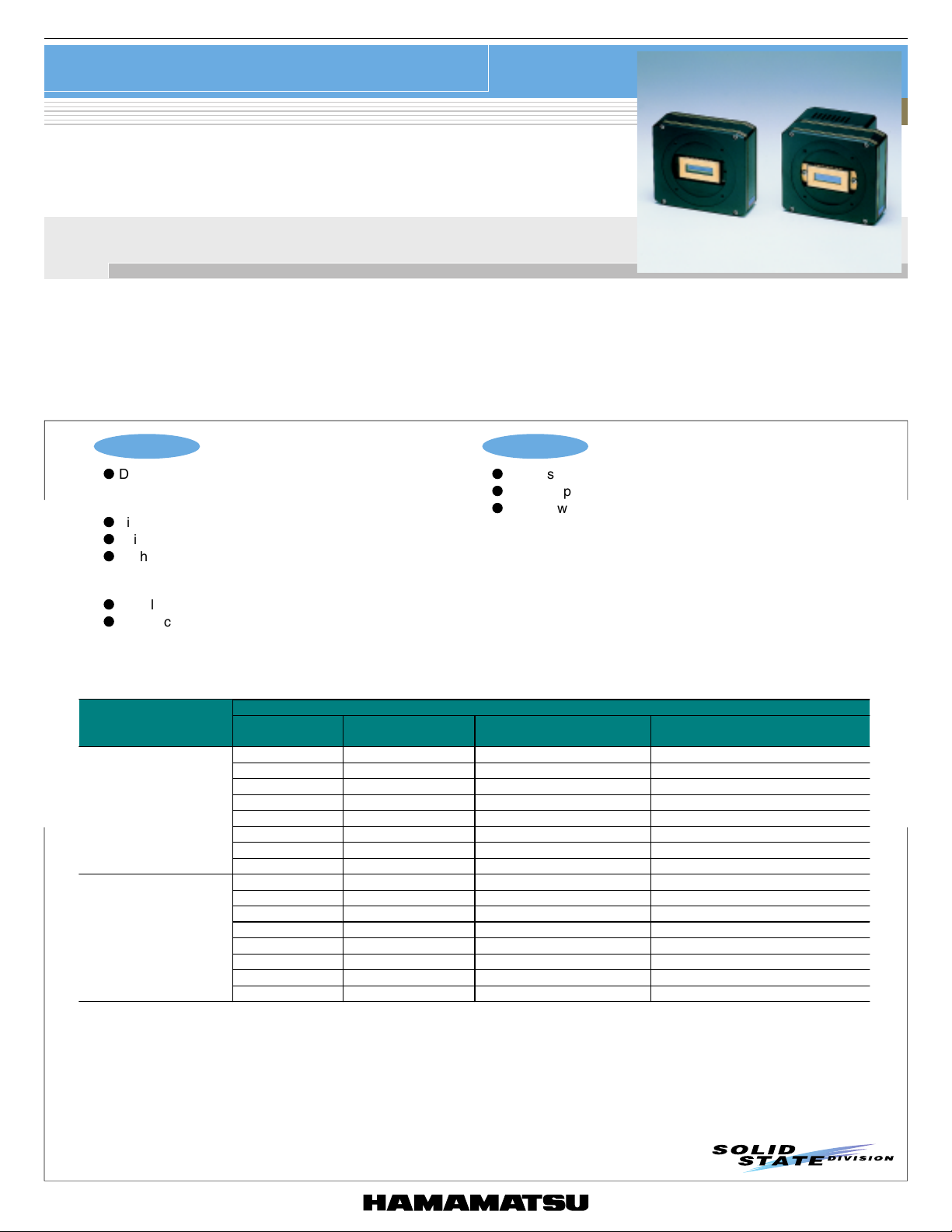
CCD multichannel detector head
C7040, C7041
Designed for back-thinned CCD area image sensor
C7040 and C7041 are high sensitivity multichannel detector heads for use with back-thinned FFT-CCD area image sensors (S7030/S7031 series)
that offer high UV sensitivity and quantum efficiency. C7040 is designed for the non-cooled back-thinned CCD image sensor (S7030 series), while
C7041 for the one-stage TE-cooled CCD area image sensors (S7031 series) for detection at even lower light levels. Both C7040 and C7041
incorporate a low-noise driver/amplifier circuit that provides reliable operation from simple external signals. C7041 also includes a highly stable
temperature controller that cools the sensor to a preset temperature level (Ts= -10 ˚C) as soon as the power is turned on. If the cooler fails and
causes internal circuitry to overheat, the built-in protection circuit automatically turns off the power to the thermoelectric cooler. Despite its
compact size, the housing configuration is designed for good heat dissipation, and threaded mounting holes on the front panel allow connections
to other devices such as monochrometers. The table below shows back-thinned CCD image sensors for C7040 and C7041. C7040 and C7041 do
not come with a CCD image sensor, so select the desired sensor and order it separately.
Features
l
Designed for back-thinned CCD area image sensor *
C7040: for non-cooled type (S7030 series)
C7041: for TE-cooled type (S7031 series)
l
Line binning operation/area scanning operation *
l
Driver/amplifier circuit for low noise CCD operation
l
Highly stable temperature controller (C7041)
Cooling temperature: -10 ± 0.05 ˚C
(Ta=10 to 35 ˚C)
l
Simple signal input operation
l
Compact configuration
1
2
Applications
l
Fluorescence spectroscopy
l
Raman spectroscopy
l
Other low-light-level detection
■ Selection guide
The table below shows CCD area image sensors applicable for C7040, C7041.
Since C7040, C7041 do not include aCCD area image sensor, so select the desired sensor and order itseparately.
Type No.
C7040
C7041
Note) CCD multichannel detector head C7042 for two-stage TE-cooled CCD area image sensor S7032 series is also available.
*1: In normal CCD image sensors that receive light from the front surface, the active area is covered with electrodes for charge transfer.
These electrodes cut off UV radiation incident on the image sensor and also reduce the quantum efficiency. In contrast, backthinned CCD image sensors have a unique structure in which the back of the active area is finely ground to allow light to enter from
the back surface. This structure ensures high UV sensitivity and quantum efficiency because incident light need not pass through the
electrodes.
*2: The FFT-CCD was originally designed as a two-dimensional image sensor. However, it can be operated like a linear image sensor
having a large active area by transferring all the pixel signals in the vertical direction to the horizontal register (this is referred to as
line binning).
Type No. Number of pixels Number of active pixels
S7030-0906 532 × 64 512 × 58 12.288 × 1.392
S7030-0907 532 × 128 512 × 122 12.288 × 2.928
S7030-0908 532 × 256 512 × 250 12.288 × 6.000
S9060-0908 532 × 256 512 × 250 12.288 × 6.000
S7030-1006 1044 × 64 1024 × 58 24.576 × 1.392
S7030-1007 1044 × 128 1024 × 122 24.576 × 2.928
S7030-1008 1044 × 256 1024 × 250 24.576 × 6.000
S9060-1008 1044 × 256 1024 × 250 24.576 × 6.000
S7031-0906 532 × 64 512 × 58 12.288 × 1.392
S7031-0907 532 × 128 512 × 122 12.288 × 2.928
S7031-0908 532 × 256 512 × 250 12.288 × 6.000
S9061-0908 532 × 256 512 × 250 12.288 × 6.000
S7031-1006 1044 × 64 1024 × 58 24.576 × 1.392
S7031-1007 1044 × 128 1024 × 122 24.576 × 2.928
S7031-1008 1044 × 256 1024 × 250 24.576 × 6.000
S9061-1008 1044 × 256 1024 × 250 24.576 × 6.000
CCD area image sensor
Active area
[mm (H) × mm (V)]
1

CCD multichannel detector head
C7040, C7041
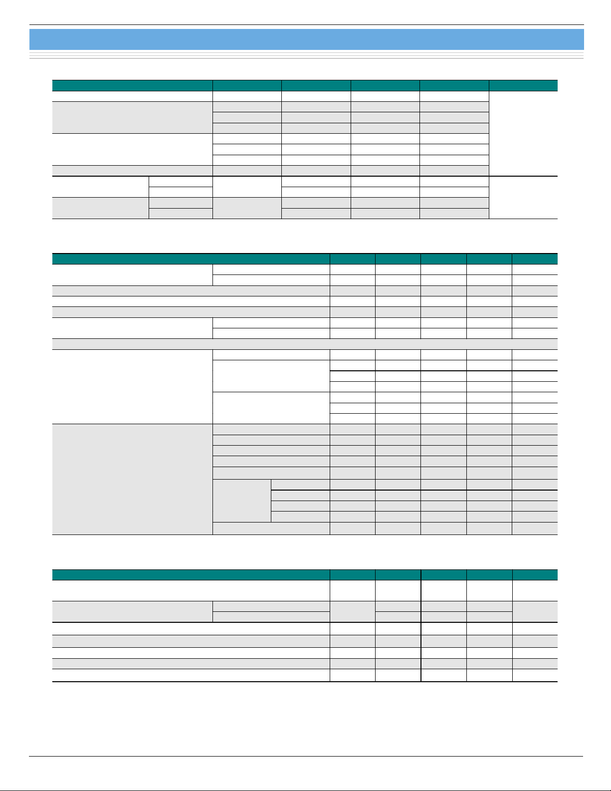
■ Absolute maximum ratings
Parameter Symbol Min. Typ. Max. Unit
Supply voltage (for digital circuitry) V
D1
V
A1+
V
A1-
V
A2
V
D2
-0.5 - +7
- - +18
- - -18Supply voltage (for analog circuitry)
- - +30
--+7
Vp - - +7Supply voltage
V
F
Digital input voltage - - - V
Operating temperature
Storage temperature
C7040 0 - +50
C7041
C7040 -20 - +70
C7041
Topr
Tstg
--+14
D (1, 2)
+10 - +35
0 - +70
■ Electrical characteristics
(Ta=25 °C, V
,
=+5 V, V
Digital input
CLK frequency f
Data video readout frequency fv - - f
Start pulse width tst 1/f
Digital output
Power supply operating conditions
Voltage
Current
)
+
=+15 V, V
)
-
= -15 V, V) =+24 V, V, =+5 V, Vp=+5 V, V.=+12 V, unless otherwise noted)
Parameter Symbol Min. Typ. Max. Unit
High level V
Low level V
High level (Io= -6 mA) V
Low level (Io=+6 mA) V
Digital circuitry V
V
V
Other
IH
IL
CLK
IH
IL
D
A1+
A1-
VA2
V
D2
Vp +4.75 +5.0 +5.25 V
V
F
+2.0 - +V
-0.5 - +0.8 V
- - 1 MHz
CLK
- - s
+2.0 - - V
--+0.8V
+4.75 +5.0 +5.25 V
+14.5 +15.0 +15.5 V
-14.5 -15.0 -15.5 VAnalog circuitry
+23.5 +24.0 +24.5 V
+4.75 +5.0 +5.25 V
+11.75 +12.0 +12.25 V
VD1 (+5 VDC) - - - +200 mA
V
(+15 VDC) - - - +100 mA
A1+
V
(-15 VDC) - - - -100 mA
A1-
VA2 (+24 VDC) - - - +30 mA
VD2 (+5 VDC) *
3
- - - +30 mA
Ta=10 °C - - +0.8 +2.5 A
Ta=20 °C - - +1.4 +2.5 A
Vp (+5 DC) *
3
Ta=30 °C - +1.8 +2.5 A
Ta=35 °C - - +2.2 +2.5 A
VF (+12 VDC) *
3
- - +100 - mA
D
/4 Hz
CLK
V
°C
V
■ Electrical and optical characteristics
(Ta=25 °C, Ts= -10 °C, V
,
=+5 V, V
Parameter Symbol Min. Typ. Max. Unit
Spectral response range
Full well capacity
Conversion gain *
Dark current *
4
5
Readout noise Nr - 20 - e-rms
Dynamic range DR - 30,000 - Photo response non-uniformity *
*3: C7041
*4: Including the circuit gain.
*5: At MPP mode. Vertical register value. The actual value equals the sum of the vertical direction because of the binning
operation.
*6: Measured at 50 % of the full well capacity.
)
+
=+15 V, V
Vertical - 300,000 Horizontal
)
-
= -15 V, V) =+24 V, V, =+5 V, Vp=+5 V, V.=+12 V)
l
Fw
-
- 600,000 -
200 to
1100
Sv - 15 - µV/e
-nm
-
e
-
DS - 50 300 e-/pixel/s
6
PRNU - - ±10 %
2
 Loading...