

HAMAMATSU C7025, C7021, C7020 Datasheet
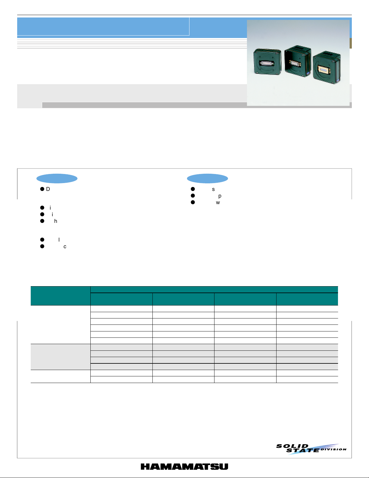
IMAGE SENSOR
CCD multichannel detector head
C7020, C7021, C7025
Designed for front-illuminated CCD area image sensors
C7020, C7021 and C7025 are high sensitivity multichannel detector heads for use with front-illuminated FFT-CCD area image sensors. C7020 is
designed for the non-cooled front-illuminated CCD image sensors (S7010 series), while C7021 and C7025 for the TE-cooled CCD image sensors
(S7011/S7015 series) for detection at even lower light levels. C7020, C7021 and C7025 incorporate a low-noise driver/amplifier circuit that
provide reliable operation from simple external signals. C7021 and C7025 also include a highly stable temperature controller that cools the sensor
to a preset temperature level (Ts= -10 ˚C) as soon as the power is turned on. If the cooler fails and causes internal circuitry to overheat, the builtin protection circuit automatically turns off the power to the thermoelectric cooler. Despite its compact size, the housing configuration is designed
for good heat dissipation, and threaded mounting holes on the front panel allow connections to other devices such as monochrometers.
The table below shows front-illuminated CCD image sensors for C7020, C7021 and C7025. C7020, C7021 and C7025 do not come with a CCD
image sensor, so select the desired sensor and order it separately.
Multichannel detector head controller C7310-02 is also available.
Features
l
Designed for front-illuminated CCD area image sensor *
C7020: for non-cooled type
C7021, C7025: for TE-cooled types
l
Binning operation *
l
Driver/amplifier circuit for low noise CCD operation
l
Highly stable temperature controller (C7021, C7025)
Cooling temperature: fixed at -10 ± 0.05 ˚C
(Ta=10 to 35 ˚C)
l
Simple signal input operation
l
Compact configuration
2
Applications
1
l
Fluorescence spectroscopy
l
Raman spectroscopy
l
Other low light level detection
■ Selection guide
The table below shows CCD area image sensors applicable for C7020, C7021, C7025.
Since C7020, C7021, C7025 do not include aCCD area image sensor, so select the desired sensor and order itseparately.
CCD area image sensor
Type No.
C7020
C7021
C7025
*1: The FFT-CCD (full frame transfer CCD) has charge transfer sections that are also used as light receiving areas, being
different from interline transfer CCD (IT-CCD) commonly used in video cameras. Compared to the IT-CCD, the FFT-CCD
offers advantages of low dark current, a 100 % open area ratio and low image lag.
*2: The FFT-CCD was originally designed as a two-dimensional image sensor. However, it can be operated like a linear image
sensor having a large active area by transferring all the pixel signals in the vertical direction to the horizontal register (this is
referred to as line binning).
Type No. Number of pixels
S7010-0906 532 × 64 512 × 60 12.288 × 1.440
S7010-0907 532 × 128 512 × 124 12.288 × 2.976
S7010-0908 532 × 256 512 × 252 12.288 × 6.048
S7010-1006 1044 × 64 1024 × 60 24.576 × 1.440
S7010-1007 1044 × 128 1024 × 124 24.576 × 2.976
S7010-1008 1044 × 256 1024 × 252 24.576 × 6.048
S7011-0906 532 × 64 512 × 60 12.288 × 1.440
S7011-0907 532 × 128 512 × 124 12.288 × 2.976
S7011-1006 1044 × 64 1024 × 60 24.576 × 1.440
S7011-1007 1044 × 128 1024 × 124 24.576 × 2.976
S7015-0908 532 × 256 512 × 252 12.288 × 6.048
S7015-1008 1044 × 256 1024 × 252 24.576 × 6.048
Number of
active pixels
Active area
[mm (H) × mm (V)]
1
CCD multichannel detector head
C7020, C7021, C7025
■ Absolute maximum ratings
Parameter Symbol Min. Typ. Max. Unit
Supply voltage (for digital circuitry) V
Supply voltage *
3
D1
V
A1+
V
A1-
V
A2
V
D2
Vp- -+7
V
F
-0.5 - +7
- - +18
- - -18Supply voltage (for analog circuitry)
- - +30
--+7
--+14
Digital input voltage - - - V
Operating temperature
Storage temperature
C7020 0 - +50
C7021, C7025
C7020 -20 - +70
C7021, C7025
Topr
Tstg
+10 - +35
0 - +70
■ Electrical characteristics
(Ta=25 °C, V
D1
=+5 V, V
Digital input
CLK frequency f
Data video readout frequency fv - - f
Start pulse width tst 1/f
Digital output
Power supply operating conditions
Voltage
Current
A1+
=+15 V, V
A1-
= -15 V, VA2=+24 V, VD2=+5 V, Vp=+5 V, VF=+12 V, unless otherwise noted)
Parameter Symbol Min. Typ. Max. Unit
High level V
Low level V
High level (Io= -6 mA) V
Low level (Io=+6 mA) V
Digital circuitry V
V
V
Other
IH
IL
clk
IH
IL
D
A1+
A1-
V
A2
V
D2
Vp +4.75 +5.0 +5.25 V
V
F
+2.0 - +V
-0.5 - +0.8 V
- - 1 MHz
CLK
- - s
+2.0 - - V
--+0.8V
+4.75 +5.0 +5.25 V
+14.5 +15.0 +15.5 V
-14.5 -15.0 -15.5 VAnalog circuitry
+23.5 +24.0 +24.5 V
+4.75 +5.0 +5.25 V
+11.75 +12.0 +12.25 V
VD1 (+5 VDC) - - - +200 mA
V
(+15 VDC) - - - +100 mA
A1+
V
(-15 VDC) - - - -100 mA
A1-
VA2 (+24 VDC) - - - +30 mA
VD2 (+5 VDC) *
3
---+30mA
Ta=10 °C - - +0.8 +2.5 A
Ta=20 °C - - +1.4 +2.5 A
Vp (+5 DC) *
3
Ta=30 °C - +1.8 +2.5 A
Ta=35 °C - - +2.2 +2.5 A
(+12 VDC) *
VF
3
- - +100 - mA
D (1, 2)
D
/4 Hz
CLK
V
°C
V
■ Electrical and optical characteristics
(Ta=25 °C, Ts= -10 °C, VD1=+5 V, V
Parameter Symbol Min. Typ. Max. Unit
Spectral response range
Full well capacity
Conversion gain *
Dark current *
4
5
Readout noise Nr - 20 - e-rms
Dynamic range DR - 30,000 - Photo response non-uniformity *
*3: C7021, C7025
*4: Including the circuit gain.
*5: At MPP mode. Vertical register value. The actual value equals the sum of the vertical direction because of the binning
operation.
*6: Measured at 50 % of the full well capacity.
A1+
6
=+15 V, V
Vertical 150,000 300,000 Horizontal
= -15 V, VA2=+24 V, VD2=+5 V, Vp=+5 V, VF=+12 V, unless otherwise noted)
A1-
l
Fw
-
300,000 600,000 -
400 to
1100
Sv - 15 - µV/e
DS - 15 45 e-/pixel/s
PRNU - - ±10 %
-nm
-
e
-
2
CCD multichannel detector head
()
C7020, C7021, C7025
■ Specifications for temperature controller (C7021, C7025)
(Ta=25 °C, V
D1
=+5 V, V
Parameter *
Cooling temperature Ts -11 -10 -9 °C
Temperature control range
Power dissipation of TE-cooler element Pp - - 7 W
Cool down time to reset temperature to - - 5 min.
Setting temperature for overheat protection To - +45 - °C
*7: Other functions include error display, automatic power off, and detection of electrical opens and shorts by the thermosensor.
A1+
=+15 V, V
7
A1-
= -15 V, VA2=+24 V, VD2=+5 V, Vp=+5 V, VF=+12 V)
Symbol Min. Typ. Max. Unit
DTs
-0.05 - +0.05 °C
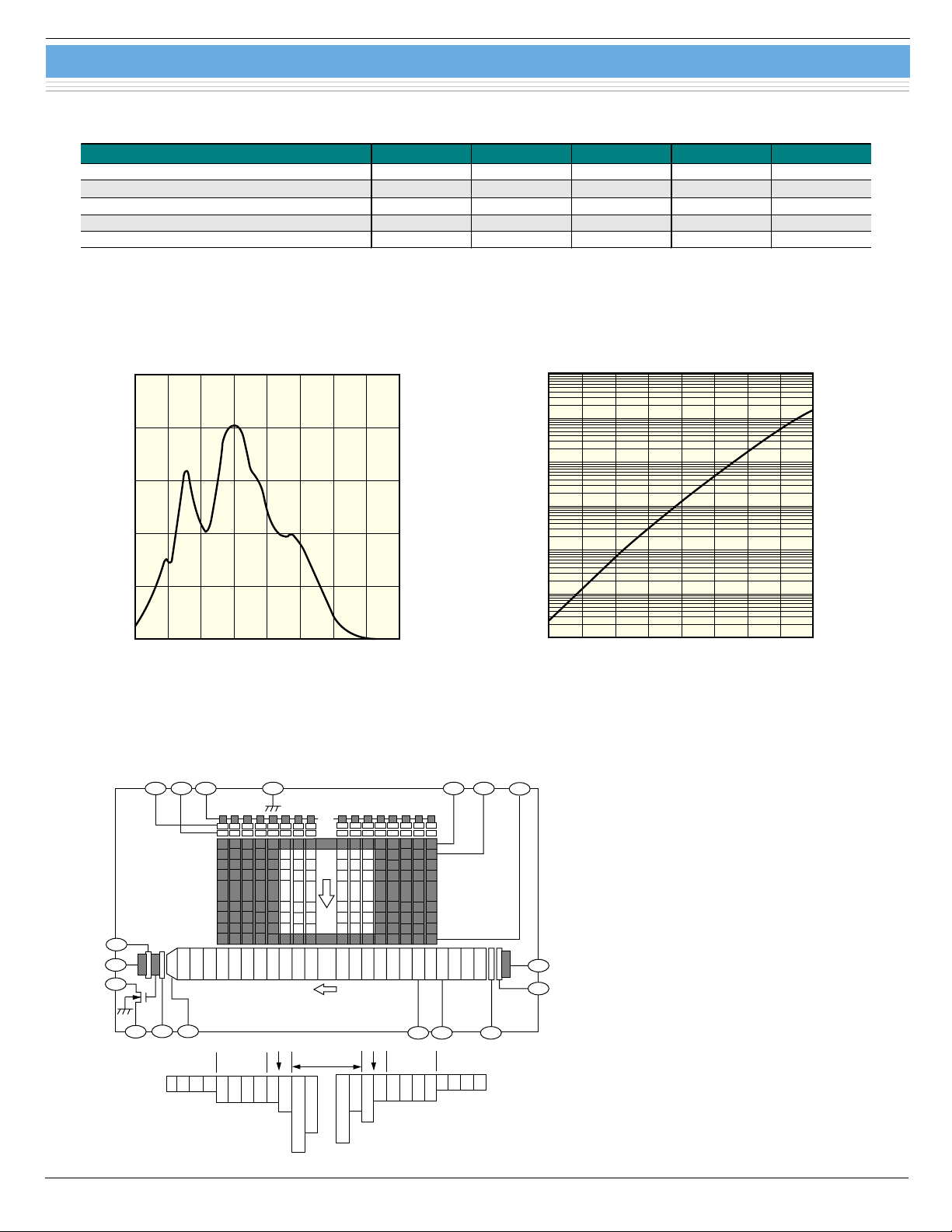
■ Spectral response
50
40
30
20
10
QUANTUM EFFICIENCY (%)
0
400 500 600 700
800 900 1000 1100 1200
(Typ. Ta=25 ˚C)
WAVELENGTH (nm)
KMPDB0051EA
■ Block diagram (front-illuminated CCD area image sensor)
IG1V
24
IG2V ISV
SS
2023 22
P1V
■ Dark current vs. temperature
10000
1000
100
/pixel/s)
-
10
1
DARK CURRENT (e
0.1
0.01
-50 -30 -20 -10
-40
P2V
15 14
TG
16
(Tentative Data)
0102030
TEMPERATURE (°C)
KMPDB0052EA
RG
1
RD
2
OS
3
45
OD OG
6
SG
4 OPTICAL
V
......
......
1H
......
2 ISOLATOIN 2 ISOLATOIN
BLACK
2n SIGNAL OUT
9
4 OPTICAL
BLACK
V=60, 124, 252
H=512, 1024
P1HP2H
4 BLANK4 BLANK
1110
IG2H
13
12
ISH
IG1H
KMPDC0015EA
3
 Loading...