HAMAMATSU C5923 Datasheet

PSD
g
g
Signal processing circuit for 1-D PSD
C5923
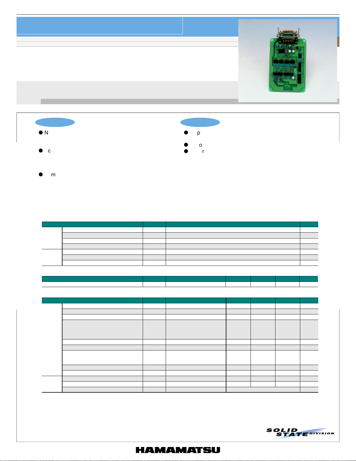
Circuit board for easier 1-D PSD operation
Features
l
No complicated adjustments required
Position can be measured just by installing a 1-D PSD on
the board.
l
Accurate position sensing
Applications
l
Displacement measurements using pulsed light synchronized
with the circuit
l
Various studies using 1-D PSD
l
Performance evaluation of 1-D PSD
Use of pulse-driven LED allows accurate position sensing
even under background light, and independent of pulsed
light intensity.
l
Compact design
An LED drive circuit, head amp, signal addition/subtraction
circuits, sample hold circuit, synchronization circuit and
analog divider circuit are mounted on a compact PC board.
Absolute maximum ratings
■
Supply voltage Vcc Max. ±18 V
Signal
processor
■
Supply voltage Vcc ±14.5 ±15 ±15.5 V
Input signal current IIN Max. Vcc Max. × 10
Output short-circuit time - Continuous s
Op erating tem perature Topr 0 to +50
Transistor c ollec tor-em itter v olta ge V
LED
Transistor collector current *
driver
Transistor collector dissipation *
Recommended operating range
Parameter Symbol Value Unit
-5
1
1
Parameter Symbol Condition Min. Typ. Max. Unit
CE
Ic 800 mA
Pc 600 mW
+30 V
A
C
°
Specifications / characteristics (Ta=25 °C, Vcc=±15 V)
■
Head amp conversion impedance *
Feedback capacitance *
Input signal current *
Rise time (outp ut 10 to 90 %) tr
Signal
processor
*1: Duty ratio: 3/10, pulse width: 90 µ s, LED: L1915-01 (made by Hamamatsu; sold separately)
*2: These resistors are lead types and inserted into sockets, so it can be easily to exchange by the user if necessary in
*3: PSD does not operate correctly if the input signal current is outside the specified range.
*4: Maximum output amplitude can be adjusted in a range of ±2 to ±10 V according to PSD type to be used.
*5: With no PSD installed and LED turned off; pulsed current of 20 µA (X1=X2) is supplied to the circuit as current
PSD reverse voltage V
Output offset voltage Vos *
Output voltage amplitude *
Output noise (analog divider) Vn All range *
Current consum ption Icc *
Transistor collector current Ic *
LED
Repetition frequency f
driver
Output method - - Open collector -
a range between 1 × 10
signal (duty ratio: 3/10, pulse width: 90 µs) that substitutes for PSD photocurrent
Parameter Symbol Condition Min. Typ. Max. Unit
2
3
4
4
to 1 × 10⁶ Ω. For m ore details, see the instruction manual that com es with the product.
2
Rf
Factory setup prior to shippin
Cf
Factory setup prior to shippin
IN
I
Photocurrent with PSD installed
Output response time
versus movem ent of light
spot position, measured
with PSD installed.
R
Factory setup prior to shipping
5
W ith PSD installed a nd
Vo
light spot falling on edge
of active area.
5
1
1
T
*
5
0.95 × 1051 × 1051.05 × 105V/A
21 22 23 pF
-5
1 × 10
30 - - µs
0514V
-10 - +10 mV
-10 - +10 V
5 10 50 mVp-p
-±45-mA
- 170 - mAp-p
- 3333 - Hz
-1 × 10⁻⁴A
1

Signal processing circuit for 1-D PSD
X
CENTER OF PSD ACTIVE AREA
LIGHT SPOT
PHOTOSENSITIVE
SURFACE
L
2
L
+
2
C5923
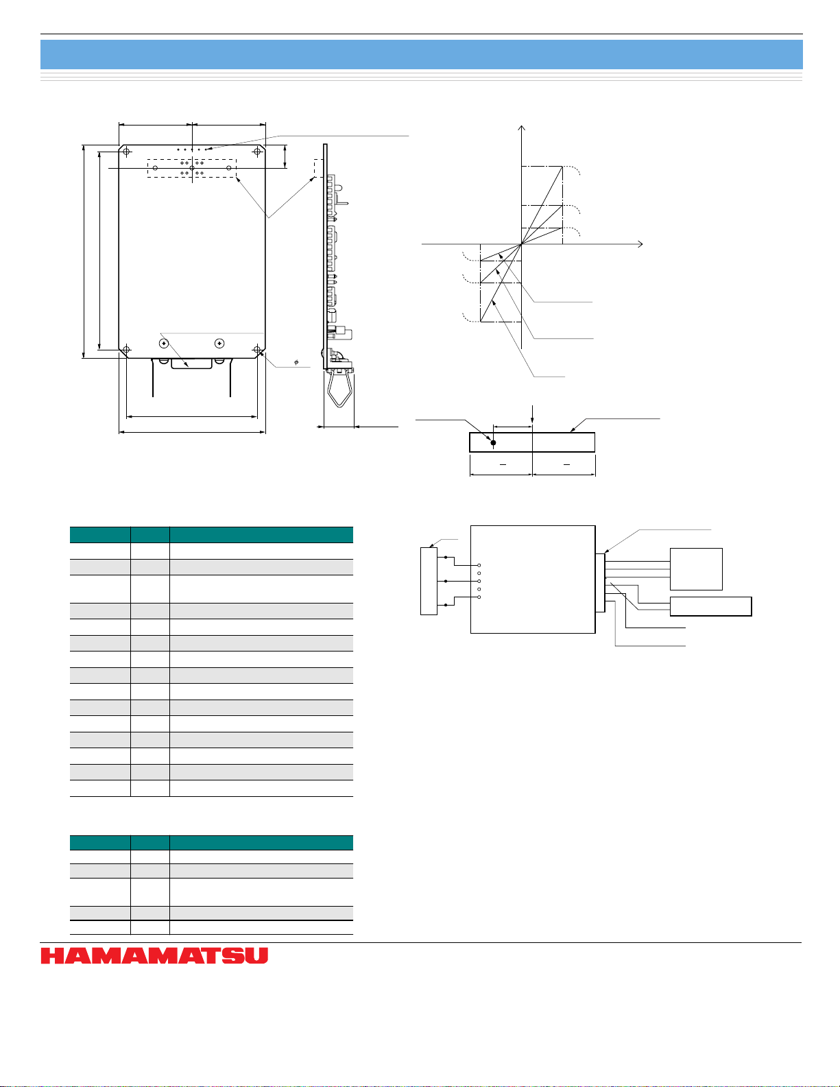
■ Dimensional outline (unit: mm, tolerance: ±0.2 mm)
37.5
12453
67
75
THROUGH HOLES FOR
EXTERNALLY CONNECTED PSD
12.5
PSD
INSTALLTION
POSITION
(4 ×) 3.2
15.5 MAX.
KACCA0054EB
110
102
37.5
D-SUB CONNECTOR
(Hirose Electric: RDAB-15P)
■ PSD and output voltage
OUTPUT Vo (V)
L
L/2
L/4
-L/2
L/2
-L/4
-L/2
S1352, S3270
-L
S3931, S3932
S3979
LIGHT SPOT POSITION X (mm)
S1352, S3931 and S3932 (PSD made by Hamamatsu) can be
directly mounted on the board. To mount other types of 1-D
PSDs, use through holes on the board.
■ Input/output terminals
D-sub connector
●
Term inal No.
Name Content
1V
REF
Reference voltage monitor output
2 VR PSD bias voltage monitor output
3Vo
4 K
5A
Divider output
(position-converted voltage)
Connection to LED or other cathode
Connection to LED or other anode
■ Operating example
PSD
X1
X2
1
C
C5923
5
+15 V
6
–15 V
7
GND
8
3
4
5
D-SUB CONNECTOR
6 +V +15 V input
7 -V -15 V input
8 G GND
9 V1 Head amp output 1
10 V2 Head amp output 2
11 V3 Subtracted signal pulse output
12 V4 Summed signal pulse output
13 V5
14 V6
Subtracted signal output after S/H *
Sum m ed signal output after S/H *
15 G GND
* S/H: sample hold
Through holes for externally connected PSD
●
Term inal No.
Name Content
1 IN1 Input from PSD output 1
2 G GND
3VR
Bias voltage output for
connection to PSD cathode
4 G GND
5 IN2 Input from PSD output 2
Information furnished by HAMAMATSU is believed to be reliable. However, no responsibility is assumed for possible inaccuracies or omissions.
HAMAMATSU PHOTONICS K.K., Solid State Division
1126-1 Ichino-cho, Hamamatsu City, 435-8558 Japan, Telephone: (81) 053-434-3311, Fax: (81) 053-434-5184, http://www.hamamatsu.com
U.S.A.: Hamamatsu Corporation: 360 Foothill Road, P.O.Box 6910, Bridgewater, N.J. 08807-0910, U.S.A., Telephone: (1) 908-231-0960, Fax: (1) 908-231-1218
Germany: Hamamatsu Photonics Deutschland GmbH: Arzbergerstr. 10, D-82211 Herrsching am Ammersee, Germany, Telephone: (49) 08152-3750, Fax: (49) 08152-2658
France: Hamamatsu Photonics France S.A.R.L.: 8, Rue du Saule Trapu, Parc du Moulin de Massy, 91882 Massy Cedex, France, Telephone: 33-(1) 69 53 71 00, Fax: 33-(1) 69 53 71 10
United Kingdom: Hamamatsu Photonics UK Limited: 2 Howard Court, 10 Tewin Road, Welwyn Garden City, Her tfordshire AL7 1BW, United Kingdom, Telephone: (44) 1707-294888, Fax: (44) 1707-325777
North Europe: Hamamatsu Photonics Norden AB: Smidesvägen 12, SE-171 41 Solna, Sweden, Telephone: (46) 8-509-031-00, Fax: (46) 8-509-031-01
Italy: Hamamatsu Photonics Italia S.R.L.: Strada della Moia, 1/E, 20020 Arese, (Milano), Italy, Telephone: (39) 02-935-81-733, Fax: (39) 02-935-81-741
2
Specifications are subject to change without notice. No patent rights are granted to any of the circuits described herein. ©2003 Hamamatsu Photonics K.K.
Measurement conditions
1. Light source: LED (λp=900 nm)
2. Light spot: φ200 µm
3. PSD: S1352 (L=34 mm)
4. PSD photocurrent: 10 µA
5. Frequency bandwidth: 10 Hz
6. Voltmeter: 195A (KEITHLEY)
7. Constant voltage power supply: ±15 V, power supply capacity:
0.2 A or more, ripple voltage: 3 mVp-p or less
When measured under the above conditions, the following output
voltage amplitude and position resolution can be obtained.
· Output voltage amplitude: V
FS=±10 V
· Position resolution: ∆l=approx. 0.6 µm (calculated value)
■ Accessories
· Connector HDAB-15S (HIROSE: For connections to power
supply and output readout device)
CONSTANT
+
VOLTAGE
–
POWER
G
SUPPLY
+
VOLTMETER
–
LED (LD) CATHODE (–)
LED (LD) ANODE (+)
Cat. No. KPSD1011E03
Apr. 2003 DN
KACCB0040EB
KPSDC0062EA
KACCC0071EA
 Loading...