HAMAMATSU C3683-01 Datasheet

PSD
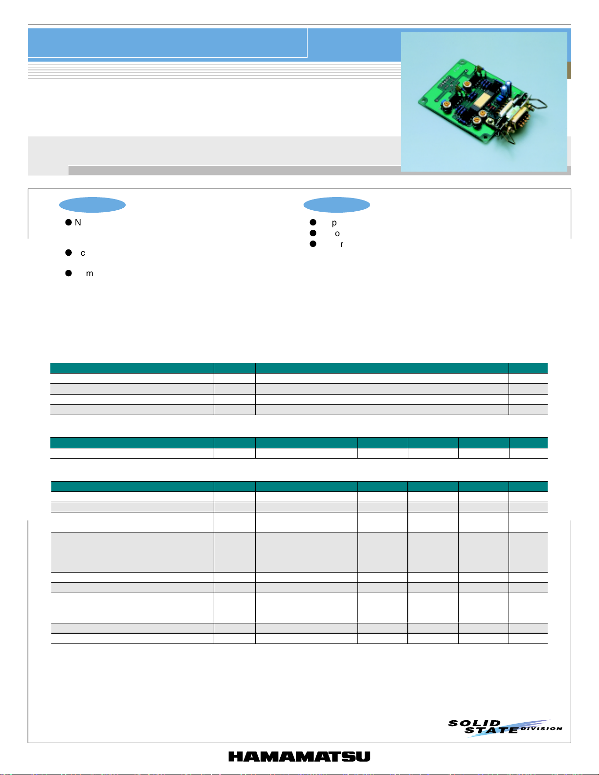
Signal processing circuit for 1-D PSD
C3683-01
Circuit board for easier 1-D PSD operation
Features
l
No complicated adjustments required
Position can be measured just by installing a 1-D PSD on
the board.
l
Accurate position sensing
Applications
l
Displacement measurements using DC light
l
Various studies using 1-D PSD
l
Performance evaluation of 1-D PSD
Position data of light spot is independent of light intensity.
l
Compact design
Head amp, signal addition/subtraction circuits, and analog
divider circuit are mounted on a compact PC board.
Absolute maximum ratings
■
Parameter Symbol Value Unit
Supply voltage Vcc Max. ±18 V
Input signal current IIN Max. Vcc Max. × 10
Output short-circuit time - Continuous s
Operating temperature Topr 0 to +50 °C
Recommended operating range
■
Parameter Symbol Condition Min. Typ. Max. Unit
Supply voltage Vcc ±14.5 ±15 ±15.5 V
Specifications / Characteristics (Ta=25 °C, Vcc=±15 V)
■
Parameter Symbol Condition Min. Typ. Max. Unit
Head amp conversion impedance *
Feedback capacitance Cf
Input signal current *
Rise time (output 10 to 90 %) tr
PSD reverse voltage V
Output offset voltage Vos *
Output voltage amplitude Vo
Output noise (analog divider) Vn All range *
Current consumption Icc *
*1: These resistors are lead types and inserted into sockets, so it can be easily to exchange by the user if necessary in a range
between 1 ×
For more details, see the instruction manual that comes with the product.
*2: PSD does not operate correctly if the input signal current is outside the specified range.
With no PSD installed, 20 µA (X1=X2) is supplied to the circuit as current signal that substitutes for PSD photocurrent
*3:
2
104 to 1 × 10⁶ Ω.
1
Rf
I
Factory setup prior to shipping
Factory setup prior to shipping
Photocurrent with PSD
IN
installed
Output respons e time
versus m ovem ent of light
spot position, measured
with PSD installed.
R
Factory setup prior to shipping
3
With PSD installed and
light spot falling on edge
of active area.
3
0.95 × 10
950 1000 1050 pF
1 ×
300 - - µs
-10 - +10 mV
-10 - +10 V
3
-5
5
-5
10
0+5+14V
- 25 - mVp-p
-±15-mA
5
1 × 10
-1 ×
1.05 × 10
10
-4
A
5
V/A
A
1

Signal processing circuit for 1-D PSD
C3683-01
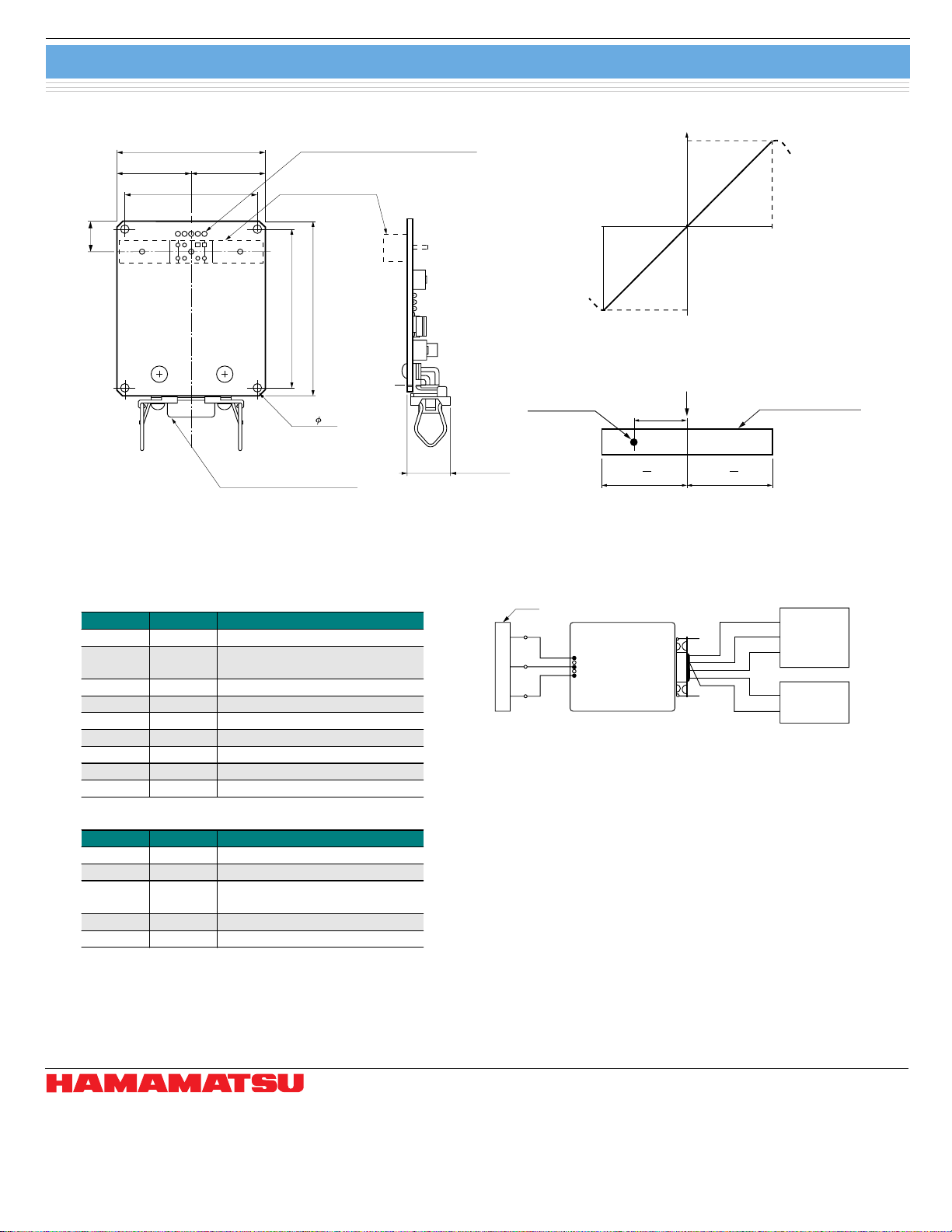
■ Dimensional outline (unit: mm, tolerance: ±0.2 mm)
THROUGH HOLES FOR
EXTERNALLY CONNECTED PSD
PSD INSTALLTION
POSITION
60
66
(4×) 3.2
11.5
28
56
28
50
54 213
D-SUB CONNECTOR
(Hirose Electric: RDEB-9P)
S1352, S3931 and S3932 (PSD made by Hamamatsu) can be
directly mounted on the board. To mount other types of 1-D
PSDs, use through holes on the board.
■ Input/output terminals
D-sub connector
●
Terminal No.
1V
2 Vo
3 -V -15 V input
4 +V +15 V input
5GGND
6 V
7V2Head amp output 2
8 V
9VASumm ed signal output
Through holes for externally connected PSD
●
Terminal No.
1IN1Input from PSD output 1
2 G GND
3V
4 G GND
5IN2Input from PSD output 2
Name Content
R
PSD bias voltage monitor output
Divider output
(position-converted voltage)
B
Subtracted signal output
1
Head amp output 1
Name Content
Bias voltage output for
R
connection to PSD cathode
■ PSD and output voltage
OUTPUT Vo (V)
+10
15.5 MAX.
KACCA0035EC
LIGHT SPOT
L
-
-
2
CENTER OF PSD ACTIVE AREA
L
2
0
LIGHT SPOT POSITION X (mm)
-10
X
L
+
2
PHOTOSENSITIVE
SURFACE
L
+
2
-
KACCC0040EA
KPSDC0062EA
■ Operating example
PSD
X1
C
X2
1
5
C3683-01
Measurement conditions
1. Light source: LED (λp=900 nm)
2. Light spot: φ200 µm
3. PSD: S1352 (L=34 mm)
4. PSD photocurrent: 10 µA
5. Voltmeter: 195A (KEITHLEY)
6. Frequency bandwidth: 10 Hz
7. Constant voltage power supply: ±15 V, power supply capacity:
0.1 A or more, ripple voltage: 3 mVp-p or less
When measured under the above conditions, the following output
voltage amplitude and position resolution can be obtained.
· Output voltage amplitude: V
FS=±10 V
· Position resolution: ∆l=approx. 0.3 µm (calculated value)
+15 V
CONSTANT
GND
VOLTAGE
Vo
GND
POWER
SUPPLY
VOLTMETER
KACCC0039EA
-15 V
4
5
3
2
5
■ Accessories
· Connector HDEB-9S (Hirose Electric: For connections to power
supply and output readout device)
Information furnished by HAMAMATSU is believed to be reliable. However, no responsibility is assumed for possible inaccuracies or omissions.
HAMAMATSU PHOTONICS K.K., Solid State Division
1126-1 Ichino-cho, Hamamatsu City, 435-8558 Japan, Telephone: (81) 053-434-3311, Fax: (81) 053-434-5184, http://www.hamamatsu.com
U.S.A.: Hamamatsu Corporation: 360 Foothill Road, P.O.Box 6910, Bridgewater, N.J. 08807-0910, U.S.A., Telephone: (1) 908-231-0960, Fax: (1) 908-231-1218
Germany: Hamamatsu Photonics Deutschland GmbH: Arzbergerstr. 10, D-82211 Herrsching am Ammersee, Germany, Telephone: (49) 08152-3750, Fax: (49) 08152-2658
France: Hamamatsu Photonics France S.A.R.L.: 8, Rue du Saule Trapu, Parc du Moulin de Massy, 91882 Massy Cedex, France, Telephone: 33-(1) 69 53 71 00, Fax: 33-(1) 69 53 71 10
United Kingdom: Hamamatsu Photonics UK Limited: 2 Howard Court, 10 Tewin Road, Welwyn Garden City, Hertfordshire AL7 1BW, United Kingdom, Telephone: (44) 1707-294888, Fax: (44) 1707-325777
North Europe: Hamamatsu Photonics Norden AB: Smidesvägen 12, SE-171 41 Solna, Sweden, Telephone: (46) 8-509-031-00, Fax: (46) 8-509-031-01
Italy: Hamamatsu Photonics Italia S.R.L.: Strada della Moia, 1/E, 20020 Arese, (Milano), Italy, Telephone: (39) 02-935-81-733, Fax: (39) 02-935-81-741
Specifications are subject to change without notice. No patent rights are granted to any of the circuits described herein. ©2003 Hamamatsu Photonics K.K.
2
Cat. No. KPSD1004E03
Apr. 2003 DN
 Loading...