HAMAMATSU C2955 Datasheet

INFRARED IC INTERNAL
TENTATIVE DATA SHEET
INSPECTION SYSTEM
C2955
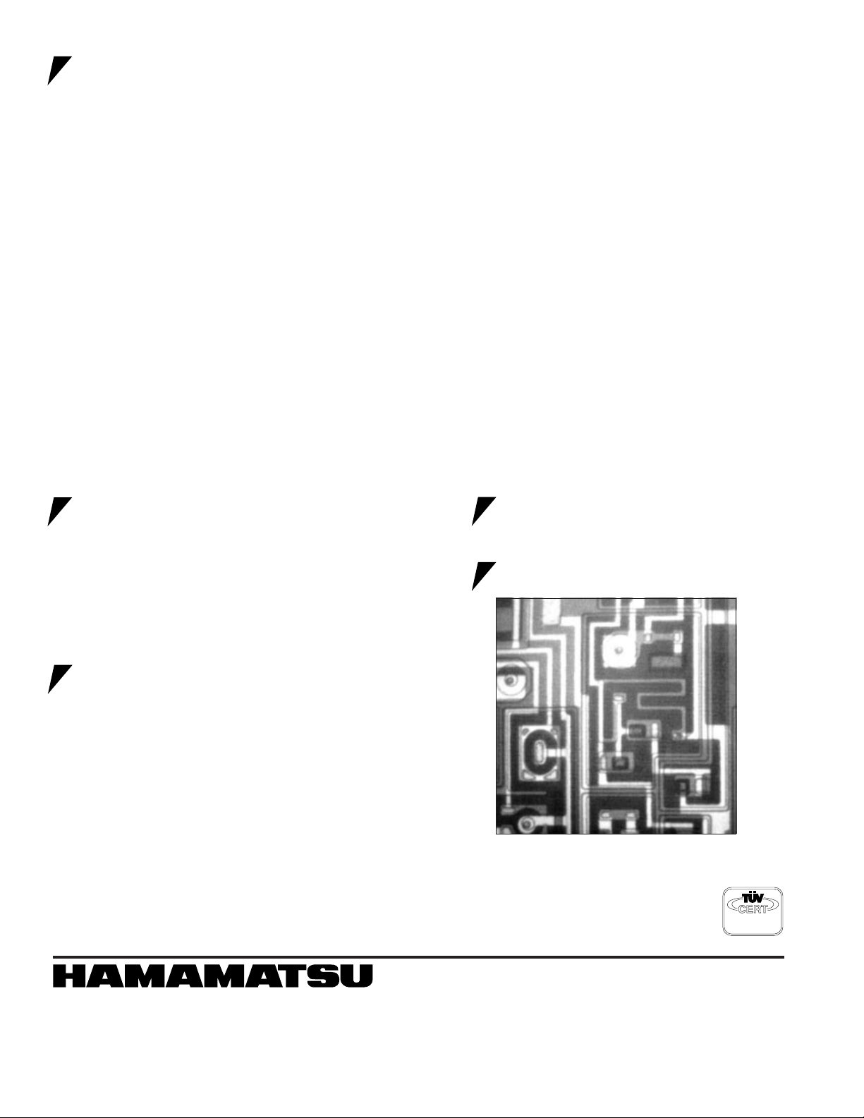
From the backside of the chip, you can see through the silicon
substrate to the patterns of the chip by means of an infrared light.
A newly developed infrared CCD camera is used to inspect pattern
images more clearly and easily than ever before.
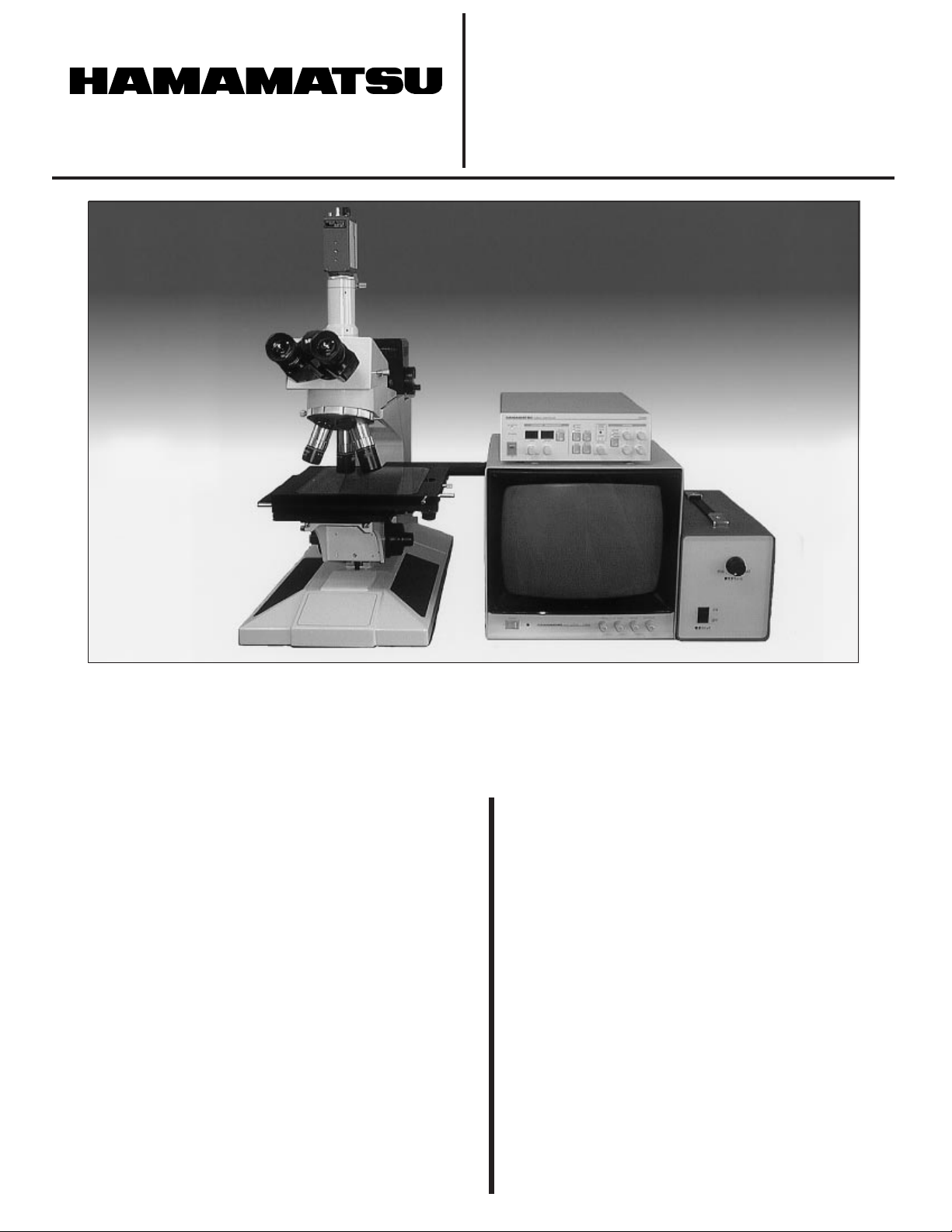
The C2955 is an IC internal inspection system incorporating an infrared microscope and an infrared CCD
camera. Use of a newly developed infrared CCD
camera enables a high sensitivity approximately ten
times that of conventional systems (in comparisons by
HAMAMATSU), at a wavelength of 1.0 µm, making it
possible to obtain sharp, clear images with high
resolution. Using an infrared light which is transmitted
through the silicon substrate enables observation of
the interconnect lines in the IC, the wire bonding
status, and the die bonding conditions, along with the
diffusion zone conditions, without damaging the part
under observation. Observation can be done from the
back side, when the sample is prepared by scraping
away the molding on the side opposite the surface of
the silicon substrate. Because the metal wiring is
never touched in the inspection process, precise
testing can be carried out under optimum conditions,
making it possible to inspect the condition of the
diffusion zones, the multilayer interconnect lines, the
Al-Si nodules wire bonding interfaces, and die bonding
details.
● Best suited for flip-chip
evaluation
● No damage to part under
observation
● High sensitivity, high
resolution
● Built-in contrast
enhancement function
● Shading correction function

SPECIFICATIONS
●Infrared CCD Camera (camera head, camera control unit)
Imaging device..............................................2/3-inch infrared CCD
Spectral response.........................................400 nm to 1200 nm
No. of pixels..................................................380,000
Effective photocathode size.........................6.3 × 4.7 mm
Power consumption.....................................20 VA
●Video Monitor
CRT...............................................................12-inch/Black and white, high-resolution model
Resolution (horizontal center)......................900 TV lines min.
Power consumption.....................................38 VA
●Infrared Microscope
Optical path switching..................................100 : 0 / 0 : 100 (eyepiece/camera)
Stage travel area..........................................153 × 153 mm
Epi-illuminated light source..........................12 V, 100 W halogen lamp
Revolver........................................................5 holes
Infrared objectives........................................10 ×, 20 ×, 50 × (optional: 5 ×, 100 × 1)
●Environmental Conditions
Ambient operating temperature range.........0 to +40°C
Ambient storage temperature range............-10 to +50°C
Ambient operating/storage humidity............90% max. (with no condensation)
Line voltage...................................................100 VAC ± 10%, 50/60 Hz
COMPONENTS
•Infrared CCD camera
OPTIONS
•C7103 IC Backside Polishing System
•Camera control unit
•Video monitor
•Infrared microscope (including light source
dimmer transformer*)
IMAGE EXAMPLE
•Cables: 1 set
* Specify the line voltage at ordering.
APPLICATIONS
•Inspection of flip-chip and other packaged IC
devices
•Testing for abnormalities (defects, failures) in
metal and polysilicon wiring
•Observation of wire bonding
•Observation of various types of die bonding zones
•Simultaneous inspection of Al-Si nodules and
multiple patterns
•Observation of pattern diffusion into substrate
•Identification of ESD failure locations
•Subject to local technical requirements and regulations, availability of products included in this promotional material may vary.
Please consult with our sales office.
•Information furnished by HAMAMATSU is believed to be reliable. However, no responsibility is assumed for possible inaccuracies
or omissions. Specifications and external appearance are subject to change without notice.
© 1999 Hamamatsu Photonics K.K.
ISO 9001/ISO 13485
EN 46001
Certificate: 09 105 79045
HAMAMATSU PHOTONICS K.K., Systems Division
812 Joko-cho, Hamamatsu City, 431-3196, Japan, Telephone: (81)53-431-0124, Fax: (81)53-435-1574, E-mail:export@sys.hpk.co.jp
U.S.A. and Canada:
Germany:
France:
United Kingdom:
North Europe:
Italy:
Hamamatsu Photonics Italia S.R.L.: Strada della Moia, 1/E 20020 Arese (Milano), Italy, Telephone: (39)02-935 81 733, Fax: (39)02-935 81 741
Hamamatsu Photonic Systems: 360 Foothill Road, Bridgewater, N.J. 08807-0910, U.S.A., Telephone: (1)908-231-1116, Fax: (1)908-231-0852
Hamamatsu Photonics Deutschland GmbH: Arzbergerstr. 10, D-82211 Herrsching am Ammersee, Germany, Telephone: (49)8152-375-0, Fax: (49)8152-2658
Hamamatsu Photonics France S.A.R.L.: 8, Rue du Saule Trapu, Parc du Moulin de Massy, 91882 Massy Cedex, France, Telephone: (33)1 69 53 71 00, Fax: (33)1 69 53 71 10
Hamamatsu Photonics UK Limited: Lough Point, 2 Gladbeck Way, Windmill Hill, Enfield, Middlesex EN2 7JA, United Kingdom, Telephone: (44)208-367-3560, Fax: (44)208-367-6384
Hamamatsu Photonics Norden AB: Smidesvägen 12, SE-171-41 Solna, Sweden, Telephone: (46)8-509-031-00, Fax: (46)8-509-031-01
Homepage Address http://www.hamamatsu.com
Cat. No. SSIS 1025E02
JUL/99 CR
Created in Japan (PDF)
 Loading...