

Page 1

TV-8888-121
NS-LCD40HD-09
(Chassis:ZORAN780)
TV
1
Page 2

WARNING
This service information is designed for experienced repair technicians only and is not designed for use
by the general public. It does not contain warnings or cautions to advise non-technical individuals of
potential dangers in attempting to service a product. Products powered b electricity should be serviced
or repaired only by experienced professional technicians. Any attempt to service or repair the product
deal with in this service information by anyone else could result in serious injury or death.
CONTENT
1. WAINING……………….……………………………………………………………………..3
2. SPECIFICATIONS…………………………………………………………………………... 6
3. LOCATION OF CONTROLS AND COMPONENTS…………………………………….. 7
3.1.Board Location……………………………….. ………………………………….…….7
3.2 Main Board…………….……………………………….. ……………………………...7
3.3 Power Board……………………………….. ………………………………………….11
3.5 LCD Panel……………………………….. …………………………………………….12
4. INSTALLATION INSTRUCTIONS………………………………………………………….14
4.1 External Equipment Connections………………………………….. ………………....14
4.2 HDMI Connections……………………………….. …………………………………….18
5. OPERATION INSTRUCTIONS……………………………………………………………..20
5.1 Front Panel Controls……………………………….. …………………………………..20
5.2 Back Panel Controls……………………………….. ………….………..……………...20
5.3 Universal Remote Controller……………………………….. …..……………………..20
6. DISASSEMBLY INSTRUCTIONS……………………………………..…………………...22
6.1 Whole Machine………………………………………………...………………………...24
6.2 Base Subassembly……………………………………………..…….………………....25
6.3 Back Subassembly…………………………………………..……….………………....26
6.4 Screen bracket Subassembly……………………………..…………………………...26
6.5 Front frame Subassembly…………………………………………….………………...27
6.6 Wire Subassembly…………………………………………………………………….…28
7. MEASUREMENTS AND ADJUSTMENTS……………………………………………..….29
8. BLOCK DIAGRAM AND CIRCUIT DIAGRAM…………………………………………….32
8.1 Block Diagram…………………………………………………………………………...32
8.2 Circuit Diagram……………………………………………………………………….….33
9. WIRING CONNECTION DIAGRAM………………………………………………………..44
10. TROUBLESHOOTING GUIDE…………………………………………………..………...45
10.1. Simple check…………………………………………………………..………….....45
10.2. PSU failure check…………………………………………………..…………….….48
10.3. Panel failure ……………..…………………………………………………………..49
2
Page 3
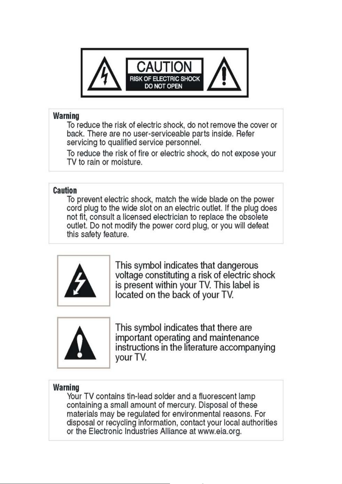
1. Warning
3
Page 4

IMPORTANT SAFETY INSTRUCTIONS
Read all of the instructions before using this appliance. When using this appliance, always exercise
basic safety precautions, including the following:
Read instructions
Read all of the safety and operating instructions before you use your TV.
Retain instructions
Retain safety and operating instructions for future reference.
Follow warnings and instructions
Follow all warnings on your TV and in the operating instructions. Follow all operating and use
instructions.
Water and moisture
Do not use your TV near water. For example, do not use it near a bath tub, wash bowl, kitchen sink,
laundry tub, in a wet basement, or near a swimming pool.
Cleaning
Unplug your TV before cleaning. Do not use liquid or aerosol cleaners. Use only a damp cloth to clean
the exterior of your TV.
Ventilation
Slots and openings in the cabinet and the back or bottom are provided for ventilation, reliable operation,
and protection from overheating.These openings must not be blocked or covered.Do not block the
openings by placing your TV on a bed, sofa, rug, or other similar surface. Do not place your TV near or
over a radiator or heat register. Do not place your TV in a built-in installation, such as a bookcase or
rack, unless you provide correct ventilation or follow the manufacturer’s instructions.
Heat
Make sure that your TV is located away from heat sources such as radiators, heat registers,stoves, or
other products (including amplifiers) that produce heat.
Grounding or polarization
Do not defeat the safety purpose of the polarized or grounding-type plug. A polarized plug has two
blades with one wider than the other. A grounding type plug has two blades and a grounding prong. The
wide blade or grounding prong are provided for your safety. If the plug does not fit, contact an
electrician to replace the
obsolete outlet.
Power cord protection
Route power cords so that they are not likely to be walked on or pinched by items placed on or against
them. Pay particular attention to cords at plugs, convenience receptacles, and the point where they exit
from your TV.
Attachments
Use only attachments recommended by Insignia.
Stand
Do not place your TV on an unstable cart, stand, tripod,bracket, or table. Your TV may
fall,causing serious personal injury and serious damage to your TV. Use only with a cart,
stand, tripod, bracket, or table recommended by the manufacturer, or sold with your TV. If you mount
your TV to the wall,follow the manufacturer’s instructions and use a mounting accessory recommended
by the manufacturer. Your TV and cart combination should be moved with care. Quick stops,excessive
force, and uneven surfaces may cause your TV and cart combination to overturn.
Lightning
For added protection for your TV’s receiver during a lightning storm, or when it is left unattended and
4
Page 5

unused for long periods of time, unplug it from the power outlet and disconnect the antenna or cable
system. This helps prevent damage to your TV from lightning and power line surges.
Servicing
Do not attempt to service your TV yourself because opening or removing covers may expose you to
angerous voltage or other hazards. Refer all servicing to qualified service personnel.
Replacement parts
When replacement parts are required, make sure that the service technician uses replacement parts
specified by the manufacturer that have the same characteristics as the original part. Unauthorized
substitutions may result in fire, electric shock, personal injury, or other hazards.
Overloading
Do not overload power outlets and extension cords because this can result in a risk of fire or electric
shock.
Object and liquid entry
Never push objects of any kind into your TV through openings because objects may touch dangerous
voltage points or short out parts that could result in a fire or electric shock. Never spill liquid of any kind
on your TV.
Damage requiring service
Unplug this TV from the power outlet and refer servicing to qualified service personnel under the
following conditions:
• When the power supply cord or plug is damaged or frayed.
• If liquid has been spilled or objects have fallen into your TV.
• If your TV has been exposed to rain or water.
• If your TV does not operate normally by following the operating instructions. Adjust only those controls
that are covered by the operating instructions because incorrect adjustment of other controls may result
in
damage and will often require extensive work by a qualified technician to restore your TV to its normal
operation.
• If your TV has been dropped or damaged in any way.
• When your TV exhibits a distinct change in performance.
Safety check
After completing any service or repair to this TV, ask the service technician to perform routine safety
checks to determine that your TV is in correct operating condition.
Power source
Operate your TV only from the type of power source indicated on the marking label. If you are not sure
of the type of power supplied to your home, consult your TV dealer or local power company.
Screen protection
Your TV’s screen is made of glass. Do not drop your TV or hit the glass screen. If the screen breaks, be
careful of broken glass. Reviewers: Please confirm.
Non-active pixels
The LCD panel contains almost 3 million thin film transistors, which provide exceptionally sharp video
quality. Occasionally, a few non-active pixels may appear on the screen as a fixed blue,green, or red
point. These non-active pixels do not adversely affect the performance of your TV, and are not
considered defects.
5
Page 6

2. Specification
Screen size 40inch
Aspect ratio 16:9
Resolution 1920x1080
Model NS-LCD40HD-09
Response Time˄ms)
Angel of view 178
Color display 16777216
NO.of preset channels 181
OSD language English
Color system NTSC/ATSC
Audio system
Audio output power(Built-in)(W) 15W×2
Audio output power(outer)(W) YES
Total power input˄W˅
Voltage range˄V˅
Power frequency˄Hz˅
Time of sleep timer(MINS) 120Min
Net weight(KG) 21.5
8(GRAY TO GRAY)
0
260W
AC110V
60Hz
Gross weight(KG) 26
Net dimension(MM) 1043*315*755
Packaged dimension(MM) 1058*330*780
6
Page 7

3. LOCATION OF CONTROLS AND COMPONENTS
3.1.Board Location
No. Parts number Description
A Board TV-5210-291 Power Board
B Board TV-5210-296 Main Board
3.2. Main Board
3.2.1 Function Description:
7
Page 8

Main Board˖
Process signal which incept from exterior equipmentˈthen translate into signal that panel can display.
Signal flowing chart
3.2.2 Connector definition
8
Page 9

Power connector(CN26)
Pin number Signal name Description
1 ON/OFF Control the power of system
2 GND Ground
3 5VSB Power of TV standby
4 GND Ground
5 GND Ground
6 12V Power of system
7 12V Power of system
IR connector (CN2)
Pin number Signal name Description
1 5V Supply the Power of bright and IR receiver
2 IR Receive IR signal
3 G Show green when TV standby
4 B Show blue when TV working
5 GND Ground
6 NC NC
Key connector(CN28)
9
Page 10

Pin number Signal name Description
1 GND Ground
2 AD0 Control Power,CH+,CH-
3 AD1 Control Menu,V+,V-,INPUT
Backlight control connector(CN22)
Pin number Signal name Description
1 BKANJ Control the backlight of pannel
2 BKEN The system turn on or turn off the backlight of TFT LCD
Panel through the power supply unit path.
3 GND GND
4 5V Not use
LVDS Signal connector(CN23)
Pin number Signal name Pin number Signal name Pin number Signal name
1 LVDS VDD 9 Not use 17 A1P
2 LVDS VDD 10 Not use 18 A1N
3 LVDS VDD 11 Not use 19 A2P
4 LVDS VDD 12 Not use 20 A2N
5 Not use 13 A0P 21 GND
6 Not use 14 A0N 22 GND
7 GND 15 GND 23 CK1P
8 GND 16 LVDS_SEL 24 CK1N
Pin number Signal name
25 A3P
26 A3N
27 GND
28 GND
29 Not use
30 Not use
AMP connector(CN20)
Pin number Signal name Description
1 18V Power of Audio power amp
2 18V Power of Audio power amp
3 GND Ground
4 GND Ground
Speaker connector(CN21)
Pin number Signal name
1 L-
2 L+
3 R-
4 R+
3.3 Power Board
3.3.1 Function Description:
10
Page 11

Supply power for Main board,Panel and DC/DC power board
3.3.2 Connector definition
CONNECTOR (CON2)
CON2 Signal name
1 24V
2 24V
3 24V
4 24V
5 24V
6 GND
7 GND
8 GND
9 GND
10 GND
CON6 Signal name
1-2 16.5V
3-4 GND
CONNECTOR (CON6)
CONNECTOR (CON4)
CON4 Signal name
1 ON/OFF
2 GND
3 5VSB
4 GND
5 GND
6 12V
7
11
3.4 LCD PANEL.
Page 12

3.4.1 Function Description:
Display the signal.
3.4.2 Connector definition
Pin No Symbol Description Note
1 Power DC 12V
2 Power DC 12V
3 Power DC 12V
4 Power DC 12V
5 Power DC 12V
6 GND GND
7 GND GND
8 GND GND
9 GND GND
10 RO[0]N ODD LVDS SINGAL-
11 RO[0]P ODD LVDS SINGAL+
12 RO[1]N ODD LVDS SINGAL-
13 RO[1]P ODD LVDS SINGAL+
14 RO[2]N ODD LVDS SINGAL-
15 RO[2]P ODD LVDS SINGAL+
16 GND GND
17 ROCLK- ODD LVDS SINGAL-
18 ROCLK- ODD LVDS SINGAL+
19 GND GND
20 RO[3]N ODD LVDS SINGAL-
21 RO[3]P ODD LVDS SINGAL+
22 NC NC
23 NC NC
24 GND GND
25 RE[0]P EVEN LVDS SINGAL-
12
Page 13

26 RE[0]N EVEN LVDS SINGAL+
27 RE[1]P EVEN LVDS SINGAL-
28 RE[1]N EVEN LVDS SINGAL+
29 RE[2]P EVEN LVDS SINGAL-
30 RE[2]N EVEN LVDS SINGAL+
CN1(Header):S14B-PH-SM4-TB(D)(LF)(JST) or equivalent.
Pin No. Symbol Description
1
2
3
4
5
6
7
8
9
10
VBL +24V Power input
GND Ground
11 NC NC
12 BLON BL ON/OFF
13 PWM Internal PWM Control
14 NC NC
4. INSTALLATION INSTRUCTIONS
4.1 External Equipment Connections
Accessories
Remote Control User Manual Battery
Antenna Connection
Generally speaking, to enjoy a clearer picture, we recommend that you use a CATV system or an
13
Page 14
outdoor antenna . location and antenna positioning
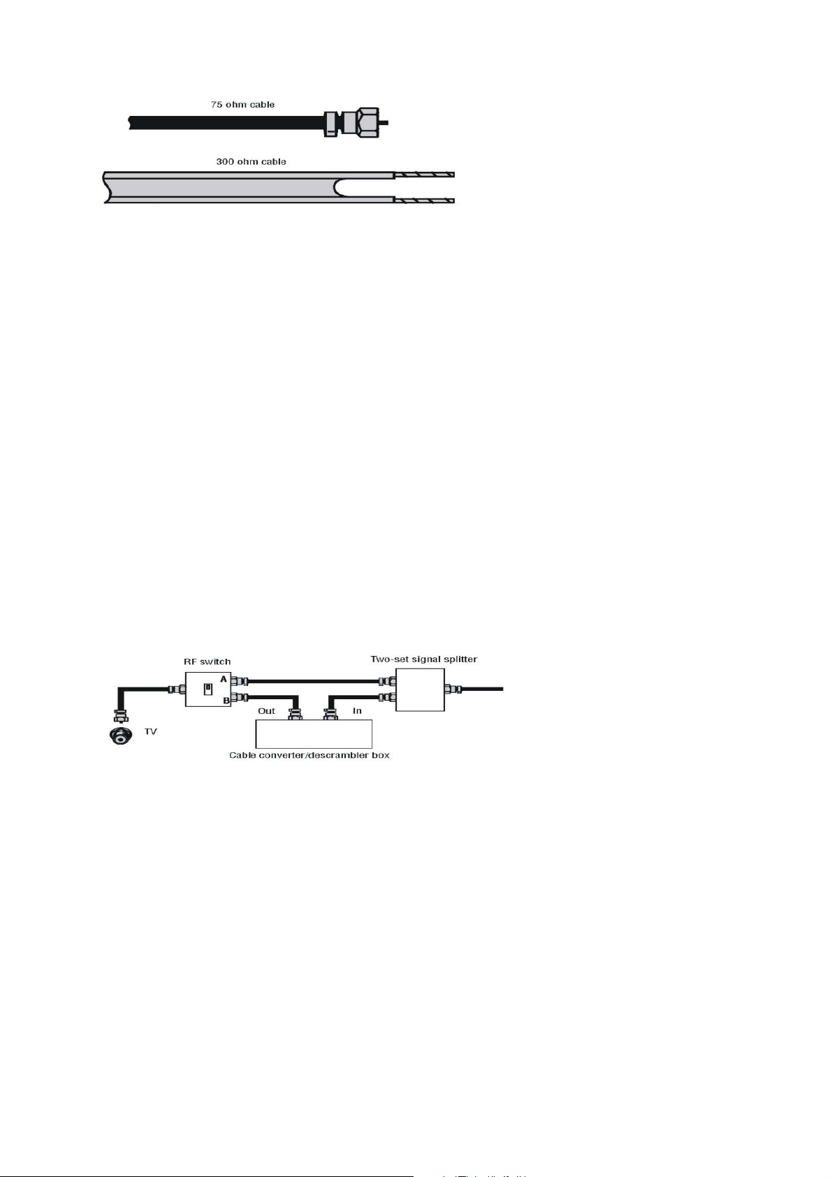
Antenna cables come in two types: 75 ohm and 300 ohm.
• If your antenna cable has a 75 ohm connector, connect the cable to the coaxial jack on the back of
your TV.
• If your antenna cable has a 300 ohm connector, connect the cable to a 300-75 ohm adapter (not
included), connect the adapter to a 75 ohm cable, then connect the other end of the 75 ohm connector
to the coaxial jack on the back of your TV.
Connecting cable TV
Your TV has a 75 ohm jack for connecting cable TV .Some cable TV providers scramble the signals
for “premium” (pay) channels. To view these channels, you need a converter/descrambler box.If you do
not have a converter/descrambler box,you can connect your cable TV directly to your TV. If you have a
converter/descrambler box, you can connect your cable TV using an RF switch (not supplied). For more
information about connecting a converter/descrambler box, contact your cable TV provider.
To connect cable TV without a converter/descrambler box:
1 Connect one end of a 75 ohm cable to the coaxial jack on the back of your TV.
2 Connect the other end of the cable to the cable TV wall outlet.
To connect cable TV with a converter/descrambler box:
• Use the following illustration to connect a converter/descrambler box. (The RF switch and the signal
splitter are not provided.) Set the RF switch to the A position to watch unscrambled channels controlled
by your TV
remote control. Set the RF switch to the B position to watch scrambled channels controlled by the
converter/descrambler controls.
External Equipment Connections
14
Page 15
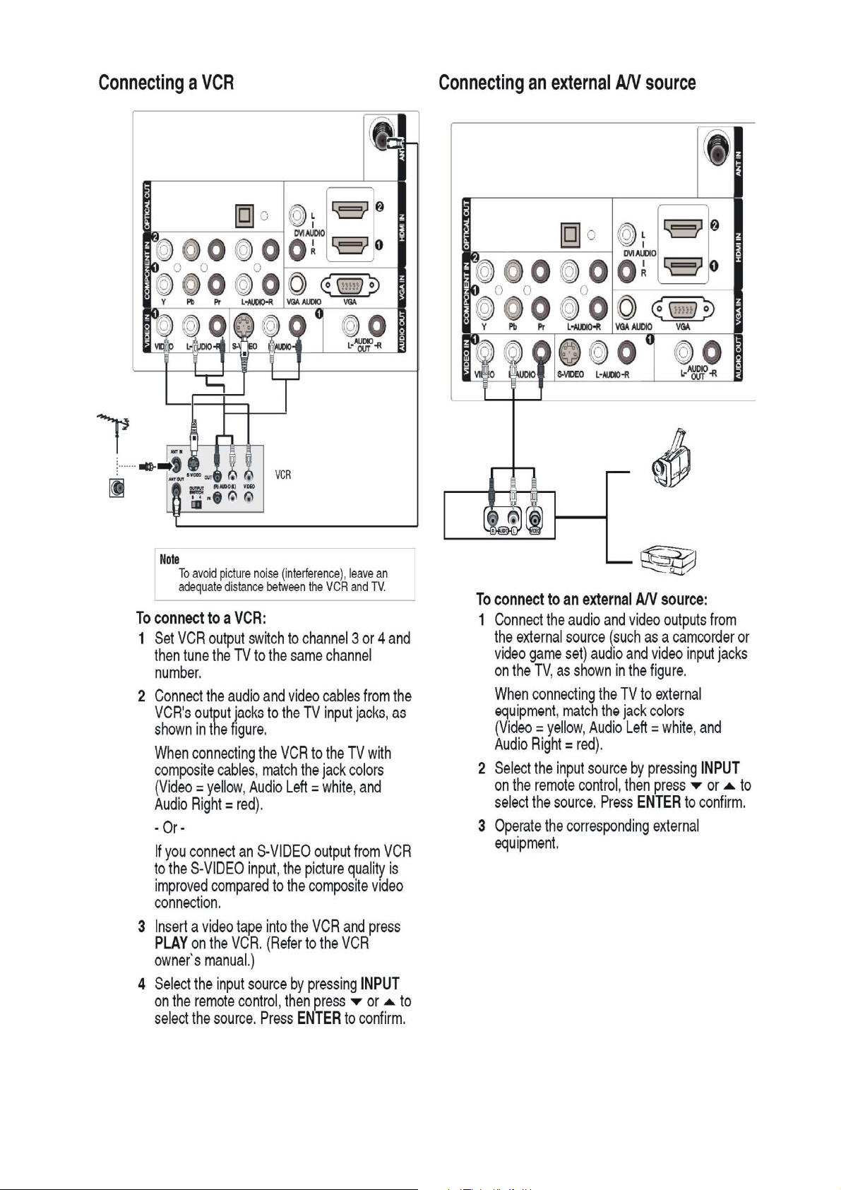
151617
Page 16

Page 17

Page 18
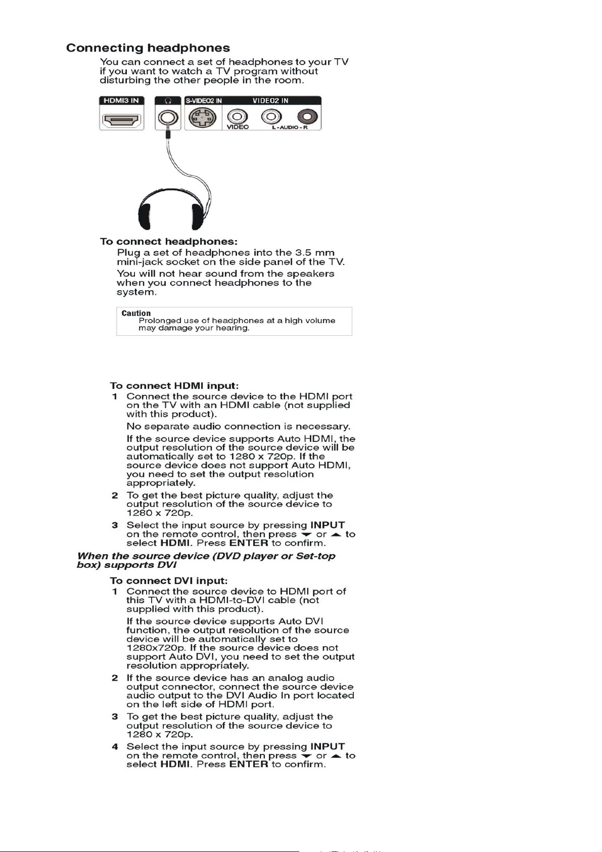
4.2 HDMI CINNECTIONS
When the source device(DVD player or Set Top Box) supports HDMI
18
Page 19

Cable sample
HDMI Cable
(not supplied with the product)
HDMI to DVI Cable
( not supplied with the product)
Analog Audio Cable
(Stereo to RCA type)
(not supplied with the product)
O USE AC POWER SOURCE
To connect your TV to a power outlet:
• Plug the power cord into a power outlet.
Notes
• Make sure that you use the correct type of power. See the label
on your TV.
• If you do not intend to use your TV for an extended period of time, unplug
the power cord from the power outlet.
• If the polarized AC cord does not fit into your non-polarized AC outlet, do
not attempt to file or cut the blade. It is your responsibility to have an
electrician replace the obsolete outlet.
• If you cause a static discharge when touching the TV and the
TV fails to function, unplug the TV from the AC outlet and plug
it back in. The TV should return to normal operation.
Wider Hole
and Blade
Polarized AC Cord Plug
AC Outlet
19
Page 20

5. OPERATION INSTRUCTIONS
5.1 Front panel controls
5.2 Back panel controls
20
Page 21
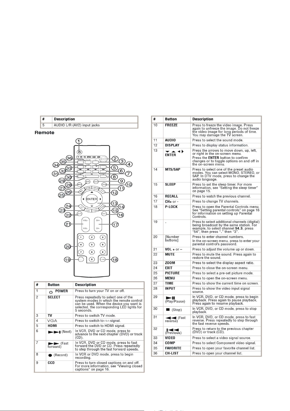
5.3 Setting Up Your Remote Control
Using the remote control
To use the remote control:
• Point the remote control towards the remote sensor on the front of your TV.
Notes
• Do not expose the remote control to shock or liquids.
• Do not use the remote control in an area with high humidity.
• Do not place the remote control in direct sunlight.
• Do not place objects, such as furniture, between the remote control and the remote sensor.
• The remote control may not work if direct sunlight or bright light shines on the remote sensor. Either
move your TV or change the angle at which you use the remote control.
21
Page 22

6. DISASSEMBLY INSTRUCTIONS
1. Remove the Back Cover
ķ Remove the twelve screws indicated
on figure above by ƻ.
ĸ Then remove the back cover from the unit.
2. Remove the Pedestal
ķ Lay down the unit so that rear
cover faces upward
ĸ Remove the four screw from the rear
cover indicated with ƻ
Ĺ Then remove the pedestal.
22
Page 23

3.Remove the power module
ķ Remove the four screws indicated on the
figure above by ƻ
ĸ Then remove the power module
4. Remove the Main board
5. Remove the speaker
Remove the four screws, take out the speaker
ķ Remove the four screws indicated on the
figure above by ƻ
ĸ Disconnected the coupler CN28ǃCN2ǃCN26ǃ
CN22ǃCN23ǃCN20ǃCN21
Ĺ Remove the Main board
6. Remove the remote control board
Remove the two screws, take out the remote control
board
6.1 whole machine
23
Page 24

The whole machine includes Packaging subassemblyǃFront-frame subassemblyǃBack-cover
subassemblyǃScreen bracket subassemblyǃBase subassemblyǃLCD panelǃPower assembly˄PSU˅ǃ
Wire subassembly.
Components List
NO Name Description Parts number
1 Accessory
2 Packaging
3 TV Set
3.1 Base subassembly TV-0250-47
3.2 Back cover subassembly TV-1300-155
3.3 Screen bracket module
3.3.1 Screen bracket assembly
3.3.2 Main Board TV-5210-296
3.3.3 PSU TV-5210-291
3.4 LCD PANEL
3.5 Front-frame subassembly TV-1300-156
24
Page 25

6.2 Base subassembly
NO Name Description
1 Base subassembly
2 Base assembly TV-0250-47
2.1 Base cover
2.2 Iron soleplate
2.3 Base support Board
2.4 Rubber PAD
3 Bolt
4 Bolt
Parts number
6.3 Back cover subassembly
1. 2.
25
Page 26

NO Name Description Parts number
1 Back cover subassembly TV-1300-155
2 Back cover assembly
2.1 Back cover
2.2 Side av label
2.3 Back jack label
2.4 Screw
6.4 Screen bracket subassembly
1. 1.1
Components List
NO Name Description
1 Screen bracket subassembly
2 Screen bracket assembly
2.1 Screen bracket
2.2 Metallic Jack Board
6.5 Front-frame subassembly
2 2.1
2.3
Parts number
2.4 2.5 5 3
26
Page 27
Components List
NO Name Description
1 Front frame module
2 Front frame assembly
2.1 Front frame TV-1300-156
2.2 Speaker Cover
2.3 Decorate ring
2.4 Power hole stopper
2.5 Key board trestle
3 Screw SJ2824-87 ST3X12F
4 Screw SJ2824-87 ST3×10F
Parts number
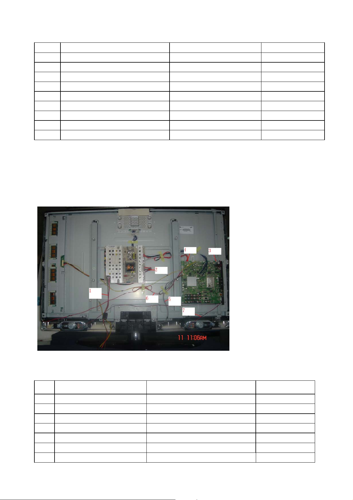
6.6 Wire subassembly---- Connection Sketch Interpretat
6.6.1. Wire Photo
6.6.2 Components List
NO Name Description
1 Power input connect wire (2139-5P)-500mm
2 24v power wire
3 LVDS wire
4 12V Power wire
5 Remote control wire
6 Key wire (PH-3)-800mm-(PH-3)
7 Speaker wire
˄TJC3-3P˅-450mm-˄TJC3-15P˅
PH7˅-350MM-(PH15)-700MM-(PH5)
27
Parts number
Page 28
7. MEASUREMENTS AND ADJUSTMENTS
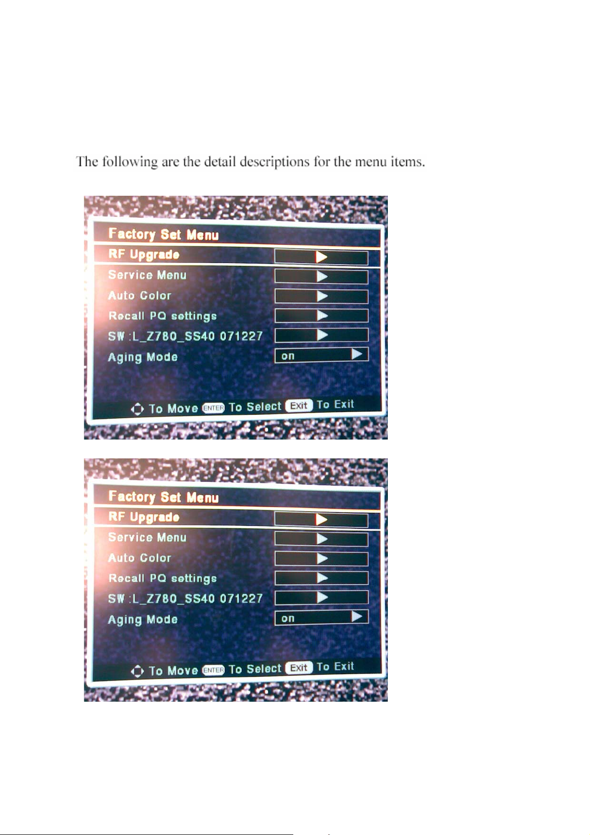
The way to the factory mode menu:
1st, adjust the volume to zero in the TV state,
2en, input 9876,
rd
3
, press “ok”
Finished these operations , system will be into the factory mode menu.
1. Factory menu
2. 1) RF Upgrade
2) Service Menu
28
Page 29

3) Auto Color
4) Recall PQ settings
5) SW:L_2780_SS40 071227
29
Page 30

6) Aging Mode
30
Page 31

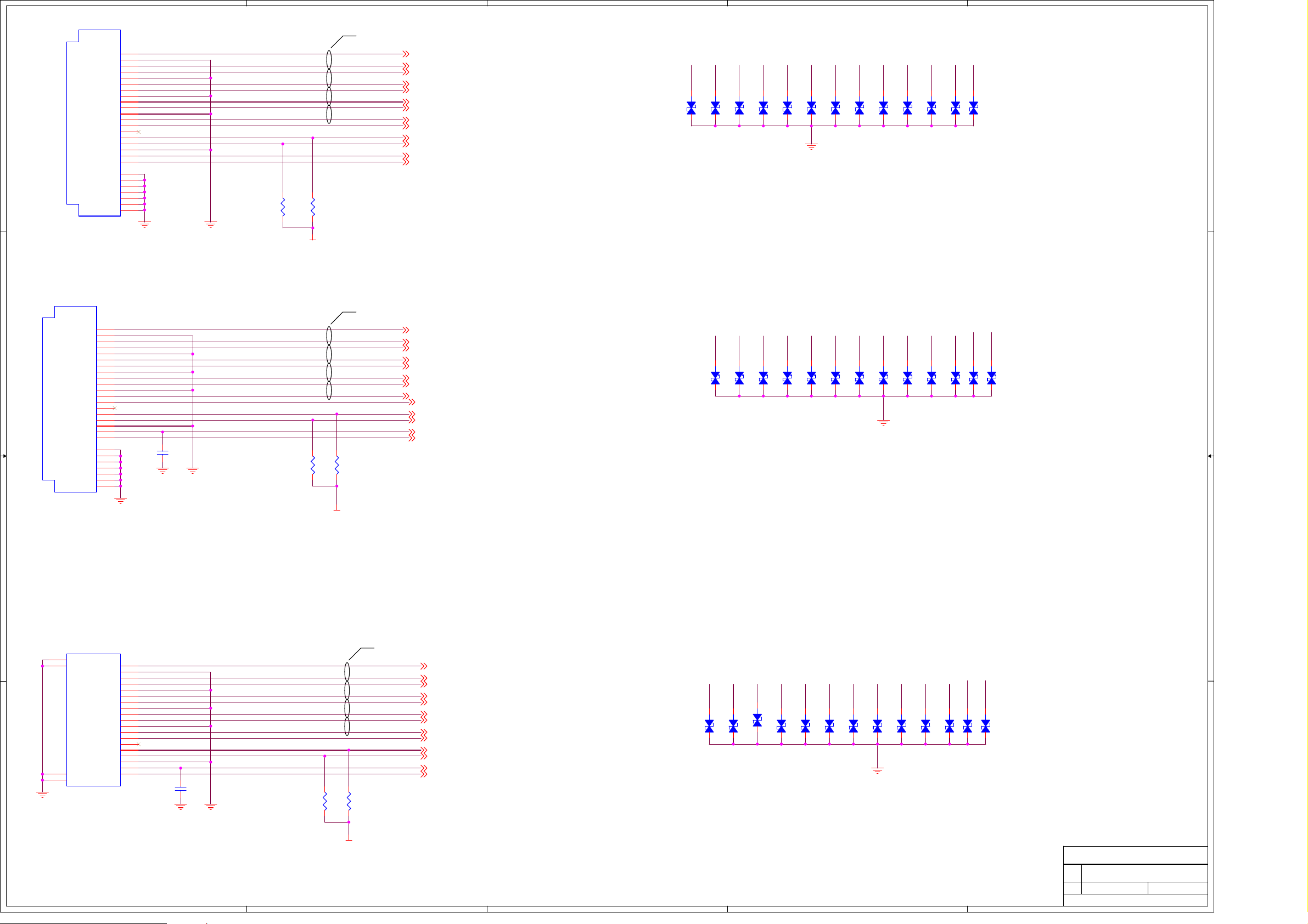
8. BLOCK DIAGRAM AND CIRCUIT DIAGRAM
8.1 BLOCK DIAGRAM
8.2 CIRCUIT DIAGRA
31
Page 32

5
D D
4
3
2
1
UA14
MCU_I2C2CLK
22
MCU_I2C2DATA
22
C C
R996 22R_DNS
R997 22R_DNS
6
SCL
5
SDA
7
IRQ/FOUT
1 2
X1 X2
VDD
VBAT
GND
ISL1208_DNS
YA3
8
3
R995 0
4
C711
0.1uF
FB29 150_Ohm_2A
1 2
C710
+
10UF/16V
3.3VSB_MCU
32.768KHz_DNS
B B
A A
Title
<Title>
Size Document Number Rev
A
<Doc>
<RevCode>
Date: Sheet
5
4
3
2
11Friday, January 18, 2008
of
1
Page 33

5
SiI9185 3:1 HDMI Switch
PCB LAYOUT: Place all decoupling
capacitors as close to the chip as
AVCC18
possible
4
DVDD18 AVCC33
12
+
C620
10uF/16V
12
PIN33
C621
100NF
SMD-R0603
PIN73
12
C622
100NF
SMD-R0603
12
100NF
SMD-R0603
PIN23
C632
12
PIN43
C633
100NF
SMD-R0603
PIN55
C634
100NF
SMD-R0603
PIN63
12
C635
100NF
SMD-R0603
+
C636
10uF/16V
3
+
C637
10uF/16V
2
1
C624
10uF/16V
Optional for HDMI CTS1
.2a
CEC Electrica
May not be req'
for
HDM
N
C
CEC_A3
12
C625
100NF
SMD-R0603
PIN
6
pec
s
IC
TS 1.
3
R770
DNS
SMD-R0603
CEC_A
UC_CEC_MCU16
PIN17
lS
d
AVCC33
1
2
3
12
C626
100NF
SMD-R0603
PIN29
D137
BAV70_DNS
UC_CEC
UC_CEC_MCU
C623
+
D D
C C
B B
+
10uF/16V
C627
100NF
SMD-R0603
PIN37
HPD04
RPWR04
DSDA_04
DSCL_04
R0XC-4
R0XC+4
R0X0-4
R0X0+4
R0X1-4
R0X1+4
R0X2-4
R0X2+4
HPD14
RPWR14
DSDA_14
DSCL_14
R1XC-4
R1XC+4
R1X0-4
R1X0+4
R1X1-4
R1X1+4
R1X2-4
R1X2+4
HPD24
RPWR24
DSDA_24
DSCL_24
R2XC-4
R2XC+4
R2X0-4
R2X0+4
R2X1-4
R2X1+4
R2X2-4
R2X2+4
R994 0
R771 0
R976 0_DNS
12
C628
100NF
SMD-R0603
12
12
PIN49
12
AVCC33
12
C629
100NF
SMD-R0603
12
R772
4.7K
SMD-R0603
PIN57
HPD0
RPWR0
DSDA_0
DSCL_0
R0XCR0XC+
R0X0R0X0+
R0X1R0X1+
R0X2R0X2+
HPD1
RPWR1
DSDA_1
DSCL_1
R1XCR1XC+
R1X0R1X0+
R1X1R1X1+
R1X2R1X2+
HPD2
RPWR2
DSDA_2
DSCL_2
R2XCR2XC+
R2X0R2X0+
R2X1R2X1+
R2X2R2X2+
12
12
SILICON IMAGE CONFIDENTIAL
A A
12
C630
100NF
SMD-R0603
12
C631
100NF
SMD-R0603
PIN69
U43
16
HPD0
32
RPWR0
30
DSDA0
31
DSCL0
18
R0XC-
19
R0XC+
21
R0X0-
22
R0X0+
24
R0X1-
25
R0X1+
27
R0X2-
28
R0X2+
36
HPD1
52
RPWR1
50
DSDA1
51
DSCL1
38
R1XC-
39
R1XC+
41
R1X0-
42
R1X0+
44
R1X1-
45
R1X1+
47
R1X2-
48
R1X2+
56
HPD2
72
RPWR2
70
DSDA2
71
DSCL2
58
R2XC-
59
R2XC+
61
R2X0-
62
R2X0+
64
R2X1-
65
R2X1+
67
R2X2-
68
R2X2+
54
CEC_A
53
CEC_D
Please contact Silicon Image prior to starting a des ign base d on th es e s ch em a tic s
6
1729374957
AVCC18
AVCC18
AVCC18
69
33
7380
AVCC18
AVCC18
AVCC18
AVCC18
DVDD18
DVDD18AGND
23
AVCC33
435563
AVCC33
AVCC33
AVCC33
SiI9185
AGND
AGND
AGND
AGND
AGND
AGND
AGND
3
9202640466066
AGND
Subject to change without notice - March 9, 2007
3.3VSB
FB24 150_Ohm_700mA
1 2
DGND
DGND
34
74
TPWR/I2CADDR
ExtSWING
TX2-
TX2+
TX1-
TX1+
TX0-
TX0+
TXC-
TXC+
TSCL
TSDA
HPDIN
I2CSEL/INT
LSCL/PSEL1
LSDA/PSEL0
RESET#
TEST
75
AVCC33
SI9185
TQFP80G
12
2
1
5
4
8
7
11
10
78
77
76
79
35
15
14
13
EXT_SW
TX2TX2+
TX1TX1+
TX0TX0+
TXCTXC+
TX_DSCL
TX_DSDA
HPDIN
TPWR/I2CADDR
NOTE: Pull-up
require for I2C
mode
I2C_SEL/INT
RESET#
12
R784
4.7K
SMD-R0603
AVCC33
R773 750
SMD-R0603
AVCC33
AVCC18
12
NOTE: Pull-down
required for slave
I2C=C0,D0,E0
12
R782
4.7K
SMD-R0603
12
R783
4.7K_NC
SMD-R0603
R785 0_DNS
SMD-R0603
R786 0
SMD-R0603
C706
47pF
12
12
12
R774
4.7K
R775
SMD-R0603
4.7K
SMD-R0603
I2C_SEL/INT 11
R988 100
R989 100
C707
47pF
close to Si9185
RESETN_AUD_HDMI 13
RESETN 13
1.8VSB
12
12
R776
4.7K
SMD-R0603
AVCC33
MCU_I2C2CLK 16
MCU_I2C2DATA 16
12
C644
+
0.1uF
12
12
R777
R778
4.7K
NI,4.7K
SMD-R0603
SMD-R0603
FB26 150_Ohm_700mA
1 2
FB27 150_Ohm_700mA
1 2
C645
100uF/16V
DVDD18
AVCC18
6
AV1_DET
UC_CEC
R779 100_DNS
HDMI_VDD14
R595 15
RUN AS 100 OHM
DIFFERENTIAL PAIRS
R780
4K7
R978
4.7K
R58
4K7
HDMI_VDD14
VCC3_3
12
R781
390_1%
HDMI_VDD
12
R979
4.7K
390_1%
HDMI_VDD
R62
U1G
B8
HDMI0_D2P
A8
HDMI0_D2N
C8
HDMI0_D1P
C9
HDMI0_D1N
A9
HDMI0_D0P
B9
HDMI0_D0N
B10
HDMI0_CLKP
A10
HDMI0_CLKN
A7
HDMI0_CEC
C10
HDMI0_SCL
E9
HDMI0_SDA
D8
HDMI0_HPD
D9
HDMI0_5VSENSE
D10
HDMI0_RXATEST
E10
HDMI0_REXT
U1O
B4
HDMI1_D2P
A4
HDMI1_D2N
C4
HDMI1_D1P
C5
HDMI1_D1N
A5
HDMI1_D0P
B5
HDMI1_D0N
B6
HDMI1_CLKP
A6
HDMI1_CLKN
C6
HDMI1_CEC
B7
HDMI1_SCL
D7
HDMI1_SDA
D6
HDMI1_HPD
C7
HDMI1_5VSENSE
E8
HDMI1_RXATEST
E7
HDMI1_REXT
HDMI I/F
ZR39780_A_6
HDMI I/F
ZR39780_A_6
Title
<Title>
Size Document Number Rev
<Doc> <RevCode>
C
11Friday, January 18, 2008
5
4
3
2
Date: Sheet
1
of
Page 34

5
4
3
2
1
S0_DQ[15..0]
U1A
S0 Memory I/F
S0_DQ15
S0_DQ14
D D
VCC1_8
R388
100_1%
R389
100_1%
C C
C503
0.1uF
C504
0.1uF
S0_DQ13
S0_DQ12
S0_DQ11
S0_DQ10 S0_A8
S0_DQ9
S0_DQ8
S0_DQ7
S0_DQ6
S0_DQ5
S0_DQ4
S0_DQ3
S0_DQ2
S0_DQ1
S0_DQ0
S0_UDM
S0_LDM
S0_VREF
B15
A21
A14
B22
B20
B17
B21
A15
B14
A22
B13
A23
B19
A18
B23
A13
A20
A19
A24
ZR39780_A_6
S0_DQ15
S0_DQ14
S0_DQ13
S0_DQ12
S0_DQ11
S0_DQ10
S0_DQ9
S0_DQ8
S0_DQ7
S0_DQ6
S0_DQ5
S0_DQ4
S0_DQ3
S0_DQ2
S0_DQ1
S0_DQ0
S0_UDM
S0_LDM
S0_VREF
S0_A13
S0_A12
S0_A11
S0_A10
S0_A9
S0_A8
S0_A7
S0_A6
S0_A5
S0_A4
S0_A3
S0_A2
S0_A1
S0_A0
S0_BA2
S0_BA1
S0_BA0
S0_UDQSN
S0_UDQS
S0_LDQSN
S0_LDQS
S0_RASN
S0_CASN
S0_WEN
S0_CKN
S0_CK
S0_CKE
S0_ODT
S1_DQ[15..0]
U1B
C14
C24
C18
D22
D18
D14
D23
D17
C19
C15
C23
C17
D19
D15
C22
C20
D21
B16
A16
A17
B18
D16
C16
D20
A12
B12
C21
C13
S0_A12
S0_A11
S0_A10
S0_A9
S0_A7
S0_A6
S0_A5
S0_A4
S0_A3
S0_A2
S0_A1
S0_A0
S0_BA2
S0_BA1
S0_BA0
S0_UDQSN
S0_UDQS
S0_LDQSN
S0_LDQS
S0_RASN
S0_CASN
S0_WEN
S0_CKN
S0_CK
S0_CKE
R391
100
R2
P7
M2
P3
P8
P2
N7
N3
N8
N2
M7
M3
M8
A8
B7
E8
F7
K7
K3
K8
K2
L1
L3
L2
L7
J8
L8
DDR II
A12
A11
A10
A9
A8
A7
A6
A5
A4
A3
A2
A1
A0
NC3
BA1
BA0
UDQS
UDQS
LDQS
LDQS
RAS
CAS
WE
CK
CK
CKE
CS
K4T51163QC-2CE7_1
U33A
DQ15
DQ14
DQ13
DQ12
DQ11
DQ10
DQ9
DQ8
DQ7
DQ6
DQ5
DQ4
DQ3
DQ2
DQ1
DQ0
UDM
LDM
VREF
ODT
B9
B1
D9
D1
D3
D7
C2
C8
F9
F1
H9
H1
H3
H7
G2
G8
B3
F3
J2
K9
S0_DQ15
S0_DQ14
S0_DQ13
S0_DQ12
S0_DQ11
S0_DQ10
S0_DQ9
S0_DQ8
S0_DQ7
S0_DQ6
S0_DQ5
S0_DQ4
S0_DQ3
S0_DQ2
S0_DQ1
S0_DQ0
S0_UDM
S0_LDM
S0_VREF
VCC1_8
Note:
The DDR II layout will also accomodate
1M bit devices, expanding the memory
footprint from 128M byte to 256M byte.
* Note:
780 MATRIX ATSC Platform
2 DDR2 32MB each, total 64MB
1080P, PIP ALL THE FEATURES
INCLUDED.
770 MATRIX ATSC Platform
1 DDR 64MB 768p and NO PIP.
C507
0.1uF
C508
0.1uF
S1 Memory I/F
S1_DQ15
S1_DQ14
S1_DQ13
S1_DQ12 S1_DQ13
S1_DQ10
S1_DQ9
B B
VCC1_8
R393
A A
100_1%
R394
100_1%
S1_DQ8
S1_DQ6
S1_DQ5
S1_DQ4
S1_DQ3
S1_DQ2
S1_DQ1
S1_DQ0
S1_UDM
S1_LDM
C505
0.1uF
C506
0.1uF
S1_VREF
R395
27
R396
51
F25
S1_DQ15
M26
S1_DQ14
E26
S1_DQ13
N25
S1_DQ12
L25
S1_DQ11
H25
S1_DQ10
M25
S1_DQ9
F26
S1_DQ8
E25
S1_DQ7
N26
S1_DQ6
D25
S1_DQ5
P26
S1_DQ4
K25
S1_DQ3
J26
S1_DQ2
P25
S1_DQ1
D26
S1_DQ0
L26
S1_UDM
K26
S1_LDM
R26
S1_VREF
B26
RDRIVER
A26
RDRIVER50
A25 D24
RTERM S1_ODT
R397
300
ZR39780_A_6
S1_A13
S1_A12
S1_A11
S1_A10
S1_A9
S1_A8
S1_A7
S1_A6
S1_A5
S1_A4
S1_A3
S1_A2
S1_A1
S1_A0
S1_BA2
S1_BA1
S1_BA0
S1_UDQSN
S1_UDQS
S1_LDQSN
S1_LDQS
S1_RASN
S1_CASN
S1_WEN
S1_CKN
S1_CK
S1_CKE
E24
R24
J24
N23
J23
E23
P23
H23
K24
F24
P24
H24
K23
F23
N24
L24
M23
G25
G26
H26
J25
G23
G24
L23
C26
C25
M24
S1_A12
S1_A11
S1_A10
S1_A9
S1_A8
S1_A7
S1_A6
S1_A5
S1_A4
S1_A3
S1_A2
S1_A1
S1_A0
S1_BA2
S1_BA1
S1_BA0
S1_UDQSN
S1_UDQS
S1_LDQSN
S1_LDQS
S1_RASN
S1_CASN
S1_WEN
S1_CKN
S1_CK
S1_CKE
R392
100
R2
P7
M2
P3
P8
P2
N7
N3
N8
N2
M7
M3
M8
L1
L3
L2
A8
B7
E8
F7
K7
L7
K3
K8
J8
K2
L8
K4T51163QC-2CE7_1
A12
A11
A10
A9
A8
A7
A6
A5
A4
A3
A2
A1
A0
NC3
BA1
BA0
UDQS
UDQS
LDQS
LDQS
RAS
CAS
WE
CK
CK
CKE
CS
DDR II
DDR II SDRAM I/F
5
4
3
U34A
DQ15
DQ14
DQ13
DQ12
DQ11
DQ10
DQ9
DQ8
DQ7
DQ6
DQ5
DQ4
DQ3
DQ2
DQ1
DQ0
UDM
LDM
VREF
ODT
B9
B1
D9
D1
D3
D7
C2
C8
F9
F1
H9
H1
H3
H7
G2
G8
B3
F3
J2
K9
S1_DQ15
S1_DQ14
S1_DQ12S1_DQ11
S1_DQ11
S1_DQ10
S1_DQ9
S1_DQ8S1_DQ7
S1_DQ7
S1_DQ6
S1_DQ5
S1_DQ4
S1_DQ3
S1_DQ2
S1_DQ1
S1_DQ0
S1_UDM
S1_LDM
S1_VREF
2
Option:
Second DDR2 could be reduced
if for ZR770 implementation
only one DDR2 will be
needed.
VCC1_8
C509
0.1uF
C510
0.1uF
Title
Matrix / HD780 Ref. Platform
Size Document
B
780_rev_A1.dsn
Sheet
221
Date:
Friday, January 18, 2008
Drawn by: S. Nguyen
Rev
of
1
A1
Page 35

5
U1C
SIO I/F
TRSTN
E16
TRST
E14
TDI
E18
TDO
E15
D D
C C
I2C_MORPH__ENA
ZR39780_A_6
B B
TMS
TCK
TAPSEL
TAPSEL_CAS
IRR
UART0_TX
UART0_RX
UART1_TX
UART1_RX
USB0_DN
USB0_DP
USB_REXT
USB_ATEST
I2C0_C
I2C0_D
I2C1_C
I2C1_D
I2C2_C
I2C2_D
SPI_DO
SPI_DI
SPI_CLK
SPI_SEL0
SPI_SEL1
SPI_HOLD
SPI_SEL2
SPI_SEL3
RESET_n
CLKIN
CLKOUT
Crystal Y1
15ppm 20C
30ppm
0-70C
E17
E13
D13
R22
L22
M22
P22
N22
D5
E5
D3
D4
AF12
AE12
AE13
AF13
AF14
AE14
R22 4K7
AA14
Y24
W25
Y25
W24
W26
Y26
AA24
AB24
V24
U26
U25
EJTCK
C1
R17 3K4_1%
R23 47
R25 47
SD_CSN
RESETN
R26
1M
R27
100
C6
27pF
68pF
I2C0CLK 9
I2C0DATA 9
I2C1CLK 5
I2C1DATA 5
I2C2CLK 10 22
I2C2DATA 10 22
RESETN 13,16
R2 4K7
R12 4K7
INFRARED_760 13
UART0TX 8,13
UART0RX 8,13
UART1TX 16
UART1RX 16
USB_DN
USB_DP
R20
4K7
VCC3_3
R610
4K7_DNS
Y1
25 MHz
C7
27pF
VCC3_3
SIO I/F
U36
1
1
R597 0
靠近
780
R597
A A
2
3
NC7SZ126
5
2
4
3
4
TRSTN
EJTDI9
EJTDO9
EJTMS9
R13 47
D139
ESD-0603_DNS
VCC3_3
RESETN
Note: Control differential
VCC3_3
impedance at 90 ohms +/15%
R21
4K7
R24 47
VCC3_3
12
12
C573
C574
0.1uF
100pF
5
R598 47
4
R90
EJTCK
SPI_WR
SPI_RD
SPI_CLK
SPI_CS_n
SPI_WEN
SPI_HOLD
XCLK 12
R54K7
R41K
R61K
R84K7
R71K
SPI_WEN 11
3
VCC3_3
EJTAG I/F
CON29
1 2
3 4
5 6
7 8
9 10
11 12
13 14
TSW-107-07-D/*NC
VCC3_3
Note:
The EJTAG I/F needed
for S/W development and
debug not for MP.
SPI_WR
SPI_RD
SPI_CLK
SPI_CS_n
SPI_WEN
SPI_HOLD
SPI_WR
SPI_RD
SPI_CLK
SPI_CS_n
SPI_WEN
SPI_HOLD
VCC3_3
R29
10K_DNS
USB_PPON12
USB_OC11
R31 1K
12
C8
0.1uF
GND
USB_DN
USB_DP
VCC3_3
C4
0.1uF
R28
10K
close to 780
SPI FLASH
32M bit
5
DIO
2
DO
6
CLK
1
CS
3
WP
7
R30 0R
R32 10k
12
C571
56pF
12
C572
56pF
HOLD
W25X32_DNS
SPI FLASH
32M bit
15
D
8
Q
16
C
9
W
1
HOLD
2
Vcc
M25P32
1 2
1 2
GND
U2
Vcc
U3
NC1
NC2
NC3
NC4S
NC5
NC6
NC7NC8
GND
12
R33 27
R34 27
8
4
C5
0.1uF
VCC3_3
3
4
5
67
11
12
1314
10
USB_VCC
C3
0.1uF
2
3
4
5
1
U4
TPS2014D
I2C0CLK
I2C0DATA
I2C1CLK
I2C1DATA
I2C2CLK
I2C2DATA
VIN1
VIN2
EN
OC
GND
R1 4K7
R3 4K7
R10 4K7_DNS
R11 4K7_DNS
R14 4K7
R15 4K7
* U2/U3 should be programmed
before soldering on PCB.
* U2/U3 will be a double footprint
and only need one of them.
6
OUT1
7
OUT2
8
OUT3
GND
15K
R969
U5
1
2
3
Rclamp0504F_DNS
R968
15K
Note: Place near
connector, and use
layout from
GND
datasheet.
2
VCC3_3
VCC3_3
VCC3_3
1
2
3
USBDMNS2
6
5
4
6
5
4
SD
C2
0.1uF
卡接口
VCC3_3
VCC3_3
12
C9
0.1UF
USBDPLS2
SPI_WR
SPI_CLK
SPI_RD
ESD-0603
R16
4.7K_DNS
SD_CSN
R611 15
R18
10K
R19 4K7
GND_POWER GND
FB1 150_Ohm_2A
1 2
12
C582
100uF/16V
D6
ESD-0603
D7
m1
M2
M5
M4
m7
m10
m18
EJTAG5 (8pin/2mm)_DNS
1
1
2
2
3
3
4
4
5
5
6
6
7
7
8
8
CNC9
SD_DET 11
SD_CSN
USB_VCCVCC5_0
12
C580
100uF/16V
CNC11
1
2
USB
3
4
USB_DNS
6 5
m15
1
M3
M6
m9
m16
m8
m17
M12
m11
m19
M13
m14
Title
Matrix / HD780 Ref. Platform
Size Document
C
780_rev_A1.dsn
Sheet
321
of
Friday, January 18, 2008
Date:
5
4
3
2
Drawn by: S. Nguyen
1
Rev
A1
Page 36
5
4
3
2
1
R736
47K
RUN AS 100 OHM
DIFFERENTIAL
PAIRS
HPD0
RUN AS 100 OHM
DIFFERENTIAL
PAIRS
RPWR1
HPD1
R0X2+ 22
R0X2- 22
R0X1+ 22
R0X1- 22
R0X0+ 22
R0X0- 22
R0XC+ 22
R0XC- 22
CEC_A 22
DSCL_0 22
DSDA_0 22
RPWR0 22
HPD0 22
R1X2+ 22
R1X2- 22
R1X1+ 22
R1X1- 22
R1X0+ 22
R1X0- 22
R1XC+ 22
R1XC- 22
CEC_A 22
DSCL_1 22
DSDA_1 22
RPWR1 22
HPD1 22
ESD-0603_0.15PF
ESD-0603_0.15PF
ESD-0603_0.15PF
R0X0+
R0X0-
D12
D13
ESD-0603_0.15PF
R1X0-
R1X1+
D124
D125
ESD-0603_0.15PF
R0X1-
R0X2+
R0X2-
D9
D8
ESD-0603_0.15PF
R1X2-
D121
ESD-0603_0.15PF
ESD-0603_0.15PF
ESD-0603_0.15PF
R0X1+
D10
D11
ESD-0603_0.15PF
R1X2+
R1X1-
D122
D123
ESD-0603_0.15PF
ESD-0603_0.15PF
ESD-0603_0.15PF
R0XC+
R0XC-
D14
D15
ESD-0603_0.15PF
R1X0+
R1XC-
D126
D127
ESD-0603_0.15PF
ESD-0603_DNS
ESD-0603_0.15PF
DSCL_0
CEC_A
ESD-0603
D16
D17
R1XC+
CEC_A
D129
D128
ESD-0603_DNS
ESD-0603
ESD-0603
RPWR0
DSDA_0
D18
DSCL_1
D130
ESD-0603
ESD-0603
HPD0
D19
D20
ESD-0603_DNS
RPWR1
DSDA_1
D131
ESD-0603
D132
HPD1
D133
ESD-0603_DNS
CON30
R0X2+
1
TMDSD2+
2
DSHLD0
TMDSD2-
TMDSD1+
DSHLD1
TMDSD1-
TMDSD0+
DSHLD2
TMDSD0-
TMDSC+
CON31
TMDSD2+
DSHLD0
TMDSD2-
TMDSD1+
DSHLD1
TMDSD1-
TMDSD0+
DSHLD2
TMDSD0-
TMDSC+
CSHLD0
TMDSC-
CEC
SCL
SDA
DDC_GND
VCC5
HPD
GND
SHLD0
SHLD1
SHLD2
SHLD3
SHLD4
GND
CSHLD0
TMDSC-
CEC
SDA
DDC_GND
VCC5
HPD
GND
SHLD0
SHLD1
SHLD2
SHLD3
SHLD4
GND
HDMI_CONN_vert
1
2
3
4
5
6
7
8
9
10
11
12
13
14
NC
15
16
17
18
19
27
20
21
22
23
24
28
D D
C C
HDMI_CONN_vert
SCL
R0X2-
3
R0X1+
4
5
R0X1-
6
R0X0+
7
8
R0X0-
9
R0XC+
10
11
R0XC-
12
13
14
NC
15
16
17
18
19
27
20
21
22
23
24
28
CEC_A
DSCL_0
DSDA_0
RPWR0 RPWR0
R38
R39
4.7K
47K
5VSB
R1X2+
R1X2-
R1X1+
R1X1-
R1X0+
R1X0-
R1XC+
R1XC-
CEC_A
DSCL_1
DSDA_1
RPWR1
C601
0.1uF
R735
4.7K
5VSB
B B
RUN AS 100 OHM
R60
47K
DIFFERENTIAL
PAIRS
HPD2
R2X2+ 22
R2X2- 22
R2X1+ 22
R2X1- 22
R2X0+ 22
R2X0- 22
R2XC+ 22
R2XC- 22
CEC_A 22
DSCL_2 22
DSDA_2 22
RPWR2 22
HPD2 22
ESD-0603_0.15PF
R2X2-
D22
D21
ESD-0603_0.15PF
ESD-0603_0.15PF
R2X1+
D23
D24
ESD-0603_0.15PF
ESD-0603_0.15PF
R2X0+
R2X0-
D25
D26
ESD-0603_0.15PF
R2X1-
R2X2+
ESD-0603_0.15PF
R2XC+
R2XC-
D28
D27
ESD-0603_0.15PF
DSCL_2
CEC_A
ESD-0603
D30
D29
ESD-0603_DNS
ESD-0603
RPWR2
DSDA_2
HPD2
ESD-0603
D31
D32
D33
ESD-0603_DNS
CON32
20
SHELL1
22
SHELL3
23
SHELL4
21
SHELL2
A A
HDMI_con
D2+
D2 Shield
D2-
D1+
D1 Shield
D1-
D0+
D0 Shield
D0-
CK+
CK Shield
CK-
CEC
DDC CLK
DDC DATA
GND
+5V
HP DET
NC
R2X2+
1
2
R2X2-
3
R2X1+
4
5
R2X1-
6
R2X0+
7
8
R2X0-
9
R2XC+
10
11
R2XC-
12
13
14
15
16
17
18
19
CEC_A
DSCL_2
DSDA_2
RPWR2
C10
0.1uF
R59
4.7K
5VSB
5
4
3
2
Title
Matrix / HD780 Ref. Platform
Size Document
C
780_rev_A1.dsn
Sheet
421
Friday, January 18, 2008
Date:
Drawn by: S. Nguyen
1
of
Rev
A1
Page 37

5
4
3
2
1
D D
VCC5_0_T2
VCC5_TUNER_IN
150_Ohm_600mA
VCC5_0_T2
TU_SDA_ph/th
TU_SCK_ph/th
IF_AGC_IN
C C
B B
C25
FB3
1 2
0.1uF
R967 4.7K_DNS
C562
C27
VCC5_0_T1
1nF
VCC5_TUNER
+
470uF/16V
C24
10uF
ALPS TUNER 5V :MAX 225MA
U39
8
+5V
2
+5V
7
Analog IF AGC
1
16
15
14
18
6
19
17
11
5
FB18
TU_SCK_ph/th
TU_SDA_ph/th
VIDEO_OUT
NC#1
AS
SDA
SCL
AGC_INT
AFT
NC
NC
NC
NC
TDQU4
300_ohm,700mA
C563
0.1uF
GND
GND
GND
GND
GND
GND
IF_OUT2
IF_OUT1
VCC5_0_T2
12
C564
1nF
I2C
ADDRESS:0xC2/0xC3
3
SIF
4
9
10
23
22
13
12
20
21
U11 DTVS205FL201A_DNS
11
5V
1
RF_AGC
2
NC_PIN2
3
NC(VT TP)
7
TP(IF Out)
8
SCL
9
SDA
10
GND
12
NC_PIN12
13
AFT
6
IF AGC
C30
C31
47pF
47pF
close to tuner
VCC3_3
R68 100
R69 100
0.1uF_25v .
C37
TU_CVBS
SIF
VIDEO OUT
DIF+
DIF-
R71
1K
IF_P_OUT
IF_N_OUT
M4
M3
M2
M1
M4
M3
M2
M1
SIF
VCC5_0_T2
R593
10K
Q31
C568 0.1uF
C567
1nF
R590
3K
VCC5_0_T2VCC5_TUNER_IN
SIF
14
TU_CVBS
15
23
22
21
20
19
18
17
16
4
5
R72
1K
10uF
R585
10K_DNS
IF_P_OUT
IF_N_OUT
IF_AGC_IN IF_AGC
I2C1DATA 3
I2C1CLK 3
C565
R589
22K_DNS
1
R982 0
R586
10K_DNS
R424 0
R423 0
close to tuner
SIF_VCM
SIF_VBIAS
SIF_RBIAS
1
R591
10K
C566
0.1uF
32
Q30
MMBT3904_DNS
R588 0R
R587
470R_DNS
C513 27pF_DNS
R422 2K
R74
5k1 .
.
MMBT3904
2 3
R592
330R
1 2
TU_CVBS_OUT
L41 0
C514 27pF_DNS
L40 0
C43
0.1uF_10v
C570
0.01uF
SIF_OUT
TU_CVBS_OUT 7
IF_P
IF_N
C22
4700pF
C42
0.1uF_10v
.
IF_P
IF_VCM
IFE_VBIAS
IF_RBIAS
IF_N
C515
30pF
VCC5_0
.
C46
0.1uF
R73
5k1
220nH
.
C14
0.1uF_16v
VCC3_3
L3
C41
0.1uF_10v
R67 47
.
.
C15
47pF_16v .
L2
BLM18AG601
R70
1K_1%
VCC3_3
R77
2K_1%
C20
10uF
Place parts very close to U1.
R425 0
R426 0
R427 47pF
R428 47pF
L4
BLM18AG601
GPIO011
VCC3_3
IF_AGC
close to U1.
C40
0.1uF_10v
.
SIF_IN_N
L1
220nH_2%_DNS
.
C17
0.1uF_16v
C38
10uF
R75 0
R76 4K7
4.7k
R421
C47
0.01uF
C16
10pF_50v_DNS
.
C18 0.1uF_10v
C21
.01uF
C516 0.01uF
C35 0.1uF_10v
VCC3_3
C19
0.1uF_16v
SIF_RBIAS
SIF_VBIAS
SIF_VCM
C517 0.01uF
IF_RBIAS
IFE_VBIAS
IF_VCM
C36
0.1uF_10v
C39
.01uF
R78
3K
AF5
AE5
AE4
AF4
AF6
AE6
AD6
AD5
AD4
AF2
AE2
AD3
AD2
AD1
AF1
AE1
AC1
AC2
AD10
AF11
AD9
AC6
AE9
AF8
AF7
ZR39780_A_6
L5
LI0603G121R
Demodulator
SIF_AINN
SIF_AINP
SIF_VREFN
SIF_VREFP
SIF_VDD3P3_0
SIF_VDD3P3_1
SIF_RBIAS
SIF_VINBIAS
SIF_VCM
IF_AINN
IF_AINP
IF_RBIAS
IF_VINBIAS
IF_VCM
IF_VREFN
IF_VREFP
IF_VDD3P3_0
IF_VDD3P3_1
DEMOD_CLKO
MPEG_FAIL
DMOD_RSTn
SA_DATA
PARAM[0]
RF_AGC
IF_AGC
U1P
DM_PLL_VDD
C49
1.0uF
C50
0.1uF
AC10
Tuner / Demodulator
A A
Title
Matrix / HD780 Ref. Platform
Size Document
C
780_rev_A1.dsn
Sheet
521
of
Friday, January 18, 2008
Date:
5
4
3
2
Drawn by: S. Nguyen
1
Rev
A1
Page 38

5
CON44
SVIDEO_AUD_R
21
RGND
SVIDEO_AUD_L
53
LGND
NC
SW
NC
RCA_LR
1 3
4
6
3RCA_SA
CON37
RGND
LGND
NC
SW
NC
RCA_LR
4
2
5
8
7
YPBPR1_AUD_R
21
YPBPR1_AUD_L
53
4
ESD-0603
VCC3_3
AV1_AUD_L
D34
AV1_AUD_R
R432
100K
ESD-0603
ESD-0603
D44
ESD-0603
D36
ESD-0603
ESD-0603
ESD-0603
D37
D45
ESD-0603
D104
D105
CVBS_IN_1 7
AV1_DET 22
D102
CON35
6
7
6
7
D D
C C
4
R476 22K
R478 22K
R79 22K
R82 22K
R97 22K
R103 22K
R479
33K
R480
33K
C52 0.47uF
R81
33K
C55 0.47uF
R84
33K
C554
0.47uF
C555
R80
100
R83
100
C65 0.47uF
R99
33K
C69 0.47uF
R107
33K
0.47uF
R481
100
R482
100
C51
1800pF
C56
1800pF
R98
100
R104
100
3
接口的开关为常通的。高电平时,有端子插入;低电平时,无端子插入
RCA
C556
1800pF
C557
1800pF
VGA AUDIO IN (A4)
CON5
C66
1800pF
C70
1800pF
PHONEJACK STEREO
1
5
2
4
12
14
15
11
U12
2Y0
2-COM
2Y1
2Y2
2Y3
1Y0
1Y1
1Y2
1-COM
1Y3
74LV4052D
8
3
5
4
2
1
7
6
VCC
INH
GND
GND
3
16
Audio_SEL0
10
A
Audio_SEL1
9
B
6
8
7
13
Audio Source Selection
AUD_SEL1
L
ESD-0603
VGA_AUD_R
ESD-0603
D41
D40
VCC8_0
C53
C54
0.1uF
10uF
AUD_SEL0
L
H
VGA_AUD_L
FB5
150_Ohm_600mA
1 2
+
R88 22K
2
AUD_OUT
NCL
AV1
YPBPR1LH
YPBPR2HH
R94 22K
C58 0.47uF
R90
33K
C63 0.47uF
R96
33K
R89
100
R95
100
VCC5_0
R414
100K_DNS
R416
100K_DNS
C60
1800pF
C64
1800pF
1
R415
100K_DNS
AUDIO_MUX_R 9
AUDIO_MUX_L 9
R417
100K_DNS
PC_R 9
PC_L 9
0.47uF
R461
100
33K
R462
100
R111
R116
33K
C75
C73
C547
1800pF
0.47uF
C548
1800pF
R110
C74
100
1800pF
C77
R113
100
1800pF
CON47
DVI_R 9
DVI_L 9
VIDEO/AUDIO IN
2
1
4 7
5
6
3RCA_H
CNC2
AV3_DNS
3
ESD-0603
R114 22K
VCC3_3
VCC3_3
ESD-0603
D42
R118 22K
R100 22K
D43
R469
4.7K
R472
4.7K
R105 22K
R471
1K
R473
1K
R117
33K
R120
33K
VCC8_0
R470
10K
Audio_SEL0
Q18
MMBT3904
VCC8_0
R474
10K
Audio_SEL1
Q19
MMBT3904
2
CNC5
DVD_L_IN
1
DVD_R_IN
2
3
DVD AUDIO IN_DNS
VCC3_3
D48
ESD-0603
D49
CVBS_IN_3 7
AV3_L_IN
ESD-0603
D50
D103
AUD_SEL011
AUD_SEL111
AV3_DET 11
R463
100K
3
8
9
AV3_DET
6
5
4
3
2
1
ESD-0603
AV3_R_IN
ESD-0603
CVBS_IN_3
AV3_L_IN
AV3_R_IN
CON38
YPBPR2_AUD_R
21
RGND
YPBPR2_AUD_L
53
NC
NC
RCA_LR
RCA_LR
LGND
4
SW
ESD-0603
ESD-0603
D47
D46
DVI_R_IN
21
RGND
DVI_L_IN
53
LGND
4
SW
ESD-0603
5
R457 22K
R459
33K
R458 22K
R460
33K
ESD-0603
D1
D2
6
7
B B
CON39
6
NC
7
NC
A A
R109 22K
R112 22K
C545
0.47uF
C546 0.47uF
4
R102
33K
R108
33K
C67 0.47uF
C71 0.47uF
C76
C79 0.47uF
0.47uF
R101
100
R106
100
R115
100
R119
100
C68
1800pF
C72
1800pF
C78
1800pF
C80
1800pF
DVD_R 9
DVD_L 9
AV3_R 9
AV3_L 9
Title
Matrix / HD780 Ref. Platform
Size Document
C
780_rev_A1.dsn
Sheet
621
Friday, January 18, 2008
Date:
Drawn by: S. Nguyen
1
of
Rev
A1
Page 39

5
CNE6
SVIDEO_DET1
4
4
3
3
2
1
D D
EJTAG6 (6pin/2.0mm)_DNS
S_C1_IN
2
S_Y1_IN
1
156
CON10
DIN4
4
8
S-Video
C C
VCC3_3
R700
100K
CON46
B B
CVBS_IN_16
536
4
DIN4
8
S-Video
CVBS_IN_36
VCC3_3
R464
100K
SVIDEO_DET 11
R131
ESD-0603
ESD-0603
ESD-0603
D99
R133
75R
SVIDEO_DET1 11
ESD-0603
D110
ESD-0603
R134
75R
ESD-0603
D111
32
LC
7
12
YC
7
D53
D54
D112
75R
R132
75R
C97 1uF
R701
75R
R702
75R
C100 1uF
C86 1uF
C92 1uF
Y_IN
C590 1uF
C591 1uF
4
C88
330pF_DNS
C93
330pF_DNS
C98
330pF_DNS
C594
330pF_DNS
C598
330pF_DNS
C102
330pF_DNS
C99
330pF
C103
330pF
C89
C94
330pF
C595
330pF
C599
330pF
330pF
Y_OUT
S_C1_OUTS_C1_IN
S_Y1_OUTS_Y1_IN
3
2
1
U1L
SD Video In
C85
0.1uF
C_OUTC_IN
C90
0.1uF
C95
0.1uF
C592
0.1uF
C596
0.1uF
C101
0.1uF
C87
47pF
C91
47pF
C96
47pF
C593
47pF
C597
47pF
C104
47pF
U3
SVIDEO0Y
V3
SVIDEO0C
W3
CVBS0
U2
SVIDEO1Y
V2
SVIDEO1C
Y3
CVBS1
ZR39780_A_6
CVBS2
Y4
A A
TU_CVBS_OUT5
5
R135
75R_DNS
C105 1uF
C107
330pF_DNS
4
C108
330pF
3
0.1uF
C106
C109
47pF
Title
Matrix / HD780 Ref. Platform
Size Document
B
780_rev_A1.dsn
Sheet
721
of
Date:
Friday, January 18, 2008
2
Drawn by: S. Nguyen
1
Rev
A1
Page 40

5
4
3
2
1
PC_UART0RX
PC_UART0TX
PR2_OUT
16
VCC
GND
8
Y2_OUT
PB2_OUT
PR1_OUT
Y1_OUT
PB1_OUT
Da
Db
Dc
Dd
VCC5_COMP
4
7
9
12
R141
75R_DNS
R142
75R_DNS
Y1_OUT
PB1_OUT
PR1_OUT
R143
75R_DNS
R980 1K
R145
75R_DNS
PC_UART0TX
UART0TX3,13
R146
75R_DNS
R147
75R_DNS
VCC3_3
R136 100
CON11
DB15ds
1
6
2
7
3
8
4
9
5
10
ESD-0603
PC_R_IN
D63
VGA_VCC5_0
PC_G_IN
ESD-0603
D64
VCC3_3
D D
D55
BZV55-C5V1
CON41
1 3
4
C C
6
3RCA_SA
D56
BZV55-C5V1
CON40
VGA_SDA
VGA_HSYNC
VGA_VSYNC
VGA_SCL
VGA_SDA
ESD-0603
VGA_SCL
ESD-0603
D59
VGA_HSYNC
VGA_VSYNC
D66
PR2_IN
PB2_IN
Y2_IN
ESD-0603_DNS
D67
COM2_DET_IN
ESD-0603_DNS
2
5
8
7
11
12
13
14
15
16 17
PC_UART0RX
PC_UART0TX
ESD-0603
ESD-0603
D60
D61
COM2_DET 11
D62
R456 100K
ESD-0603
PC_B_IN
R149
75
PC_B_IN
D65
PC_R_IN
PC_G_IN
R150
75
R151
75
R169
75
ESD-0603
Y1_IN
R170
75
C1121uF
C1161uF
C1191uF
ESD-0603
PB2_IN
PR1_IN
ESD-0603
PR2_IN
ESD-0603
ESD-0603
D73
D72
PB1_IN
ESD-0603
D70
D71
C1251uF
C1271uF
C1281uF
Y2_IN
ESD-0603
D69
D68
R171
75
VCC5_0
R140 20K_DNS
R144 10K_DNS
VCC5_0
R148 20K_DNS
R152 10K_DNS
COM2_DET_IN
COM1_DET_IN
ESD-0603
D100
VCC5_0
R162 20K_DNS
R163 10K_DNS
VCC5_0
R165 20K_DNS
R167 10K_DNS
VCC5_0
R172 20K_DNS
R173 10K_DNS
R138
D101
VCC5_0
20K_DNS
R139 10K_DNS
2
3
5
6
11
10
14
COMP_VIDEO_SW1
13
1
15
C121
0.1uF
U13
S1a
S2a
S1b
S2b
S1c
S2c
S1d
S2d
IN
#EN
PI5V330
C115 0.22uF
C117 0.22uF
C118 0.22uF
R981 1K
R490
4.7K_DNS
R137 100
R594 0_DNS
Close to U1
C1100.22uF
C1110.22uF
C1130.22uF
RGB_VSYNC
RGB_HSYNC
C120 1000pF
R620 0_DNS
Q29
2N7002LT1
1
C1141000pF
2 3
1
VCC3_3
R493
4.7K
23
Q28
MMBT3906
V4
VIN_R1
U4
VIN_G1
T3
VIN_B1
R4
SOGIN0
T4
SOYIN0
T5
VGA_R0
R5
VGA_G0
R3
VGA_B0
L5
AFE_VS_IN
K5
AFE_HS_IN
UART0RX 3,13
R491 100
PC_UART0RX
U1F
HD Video In
ZR39780_A_6
VGA_UART_ON/OFF 16
Da
Db
Dc
Dd
VCC5_COMP
C132
10uF
VCC5_COMP
4
7
9
12
C133
0.1uF
VGA_SDA
VGA_SCL
Y2_OUT
PB2_OUT
PR2_OUT
R175 4K7
R177 4K7
U15
24LC02B
5
SDA
6
SCL
1
A0
2
A1A2GND
Vcc
WP
8
3
7
4
COM_Y2_IN
COM_CB2_IN
COM_CR2_IN
R180
VGA_HSYNC
VGA_VSYNC
COMP_VIDEO_SW1
COMP_VIDEO_SW2
R164 0
R166 0
R168 0
BAV70
100
D74
1
3
2
R186 100
R189 100
R190 100
R191 100
Y2_OUT
PB2_OUT
PR2_OUT
VGA_VCC5_0
RGB_HSYNC
RGB_VSYNC
COMP_SW1
COMP_SW2
5VSB
R187
4.7K
VCC3_3
R188
4.7K
RGB_VSYNC 16
COMP_SW1 11
COMP_SW2 11
1 3
4
6
3RCA_SA
B B
INNER DVD_YPBPR
PR1_IN
2
PB1_IN
5
Y1_IN
8
COM1_DET_IN
7
CNC4
7
7
6
6
5
5
4
4
3
3
2
2
1
1
TJC3-7A (7pin/2.0mm)_DNS
ESD-0603
C1221uF
COM1_DET 11
R455 100K
CR_DVD
CB_DVD
R466 4.7K
ESD-0603
CB_DVD
Y_DVD
ESD-0603
D77
D76
CR_DVD
D75
VCC3_3
Y_DVD
VCC3_3
R174 100
AUTO_SW 11
R181
R182
75
75
R183
75
R159
75
R160
75
R161
75
C1291uF
C1301uF
C1311uF
C1231uF
C1241uF
VCC5_0
R153 20K_DNS
R154 10K_DNS_DNS
VCC5_0
R155 20K_DNS
R156 10K_DNS
VCC5_0
R157 20K_DNS
R158 10K_DNS
VCC5_0
R176 20K_DNS
R178 10K_DNS
VCC5_0
R179 20K_DNS
R420 10K_DNS
VCC5_0
R184 20K_DNS
R185 10K_DNS
C126
0.1uF
COM_Y2_IN
COM_CB2_IN
COM_CR2_IN
COMP_VIDEO_SW2
VCC5_0
2
3
5
6
11
10
14
13
1
15
PI5V330_DNS
FB6 150_Ohm_600mA
1 2
Analog Video Inputs
S1a
S2a
S1b
S2b
S1c
S2c
S1d
S2d
IN
#EN
U14
16
VCC
GND
8
HD Analog Inputs
A A
5
4
3
2
COMP_SW1
COMP_SW2
Level
L VGA
H
H
COMPONENT_OUT
COMPONENT1
COMPONENT2L
INNER DVD
Title
Matrix / HD780 Ref. Platform
Size Document
C
780_rev_A1.dsn
Sheet
821
Friday, January 18, 2008
Date:
Drawn by: S. Nguyen
1
of
Rev
A1
Page 41

5
VCC3_AUD
1 2
FB7
150_Ohm_600mA
D D
I2S_SCLK
I2S_LR_CLK
R226
R229
15K_DNS
C210 0
C211 0
CON45
HEADPHONE_OUT
DVD_L6
DVD_R6
R223
100K
15K
R231
10K
1
2
367
4
5
I2S_DATA0
AV_L_OUT
AV_R_OUT
1 2
8V_AMP
R225
10K
R236
10K
HEADPHONE OUT
PHONE_OUT_R
HEADPHONE_PLUG
PHONE_OUT_L
Sc4_in_L
Sc4_in_R
C194
470pF
1
2
3
4 5
LM4558
+
C209
10uF/16V
D82
ESD-0603_DNS
12
R224
100K
U18
OUTA
INAINA+
VSS INB+
ESD-0603_DNS
OUTB
R200
10K_DNS
EJTMS 3
EJTDI 3
EJTDO 3
RGND
LGND
SWNCNC
FB10
VCC3_3
R201
R199
R202
10K
10K
10K
I2S_MCLK
I2S_SCLK
I2S_LR_CLK
I2S_DATA0
21
53
4
ESD-0603
ESD-0603
D79
D80
C204
+
PHONE_OUT_R
470uF/16V
8V_AMP
12
+
C207
47uF/16V
SMD470UF/16V
R228
1K
C208
0.1uF
LS_HP_R
LS__HP_L
8
U1E
Audio I/F
ZR39780_A_6
C C
B B
LRCLK0
ADATAI0_0
ADATAI0_1
ADATAI0_2
ADATAO0_0
ADATAO0_1
ADATAO0_2
IEC958_0
R204 22
AF15
ACLK0
R205 22
AE15
BCLK0
R206 22
AE16
AD15
AC16
AB16
R207 22
AD16
AC17
AB17
IEC958_O
AF16
CON34
6
7
RCA_LR
VCC8_0
150_Ohm_600mA
VDD
INB-
3.3VSB
D83
C135
10uF
10uF/16V
10uF/16V
1 2
C167
C169
ESD-0603_DNS
C161
+
+
AV_R_OUT
AV_L_OUT
8
7
6
R240
100K
8V_AMP
D84
VCC1_8_AUD
0
C165 0
12
C195
470pF
R227 15K
R235
10K
HEADPHONE OUT
HEADPHONE_PLUG 11
VCC1_8_AUD
VCC1_8_AUD
VCC1_8_AUD
C152
100nF
C156
R20910K
R210
220
R211
220
VCC8_0
1 2
150_Ohm_600mA
AUDIO OUTPUT
470uF/16V
R232
SMD470UF/16V
15K_DNS
C136 27pF
C137 27pF
1 2
FB17
150_Ohm_600mA
1uF
FB9
C171
10uF
C205
+
HEADPHONE_PLUG
76
77
78
79
80
81
82
83
84
85
86
87
88
89
90
91
92
93
94
95
96
97
98
99
100
PHONE_OUT_L
R233
1K
PHONE_OUT_R
PHONE_OUT_L
Y2
27 MHz
C553
C142
330uF
100nF
C143
100nF
I2S_MCLK
75
I2S_SCLK
I2S_LR_CLK
I2S_DATA0
I2S_DATA1
I2S_DATA2
I2S_DATA3
I2SA_SCLK
I2SA_LR_CLK
I2SA_DATA
VDD18
VSS18
BUS_EXP
IRQ
GND_PSUB
NC
NC
NC
NC
NC
NC
NC
NC
MONO_IN
SC4_IN_L
SC4_IN_R
SC1_OUT_R
SC1_OUT_L
1
C172
100nF
C549
330PF
330PF
CNC10
4
4
3
3
2
2
1
1
TJC3-4A(4pin/2.5mm)_DNS
4
SPDIF_OUT
IEC958_O
RESETN_AUD_HDMI 16
R193 100
R195 100
VCC3_AUD
L13
100uH
C162 0
C168 0
1uF
C176 1uF
AV3_R 6
AV3_L 6
C185
47uF
Gain
VCC12_0
VCC12_0
12
+
D87
D81
L12
100uH
L14
100uH
C166 0
C170 0
MAIN_R
R234
47K_DNS
1N4148
R245
R249
10K
L11
100uH
L15
10uH
MAIN_L
1 2
R243 4.7K
10K
AMP_SD16
VCC3_AUD
R230
47K_DNS
1 2
C141
150_Ohm_600mA
330uF
10nF
Sc3_in_R
Sc3_in_L
Sc2_in_R
Sc2_in_L
VCC3_AUD
1
R992
10K_NC
1 2
FB8
C148
10nF
C153
C155
10nF
Sc5_in_R
Sc5_in_L
23
Q2
MMBT3906
R246
R974 100_DNS
R975 100_DNS
C145
10nF
C1471uF
0
MAIN_R
C151
0
C154
PC_R 6
PC_L 6
AUDIO_MUX_R 6
AUDIO_MUX_L 6
4.7K
3.3VSB
R251
4.7K
1 2
D88 1N4148
C1441uF
LS__HP_L
MAIN_L
+
C216
220uF/16V
D85 1N4148
D86 1N4148
RESET
R194
270K
C138
100nF
C139
C140
100nF
100nF
5859606162636465666768697071727374
51525354555657
U16
C146
SCL
SDL
RST
VSS18
VDD18
CK_SEL
I2S0_SCLK
VSS33_IO1
VSS33_IO2
VDD33_IO2
I2S/PCM/CLK
SC3_OUT_L
GND_H
VCC_H
C550
VDD33_IO1
SPDIF_OUT
I2S0_DATA0
VCC18_CLK1
VCC18_CLK2
GND18_CLK1
GND18_CLK2
CK_TST_CTRL
SPDIF_BYPASS
XTALIN_CLKXTP
XTALOUT_CLKXTM
STV8358D-GP
SC2_OUT_R
SC2_OUT_L
GND33_LS
VCC33_LS
SC2_IN_R
SC2_IN_L
VBG
VREFA
SC1_IN_R
SC1_IN_L
GND33_SC
VCC33_SC
SC3_OUT_R
SC5_IN_L
SC5_IN_RNCNC
18171615141312111098765432
19202122232425
C173
100nF
C177
C178
10uF
100nF
C184
100nF
I2S0_DATA1
I2S0_LR_CLK
VDD18_CONV
VSS18_CONV
VDD33_CONV
VSS33_CONV
GND_SANCNC
I2SD_DATA
HP_LSS_R
HP_LSS_L
SC3_IN_R
330PF
C179
10uF
ADR_SEL
HP_DET
LS_SUB
SCR_FLT
SCL_FLT
SC3_IN_L
C551
C182
100nF
50
VDD18
49
VSS18
48
47
46
45
44
NC
43
NC
42
41
NC
40
39
NC
38
37
NC
36
LS_R
35
NC
34
LS_L
33
NC
32
LS_C
31
30
29
28
27
26
C159
100nF
C552
330PF
C180
100nF
0
C183 0
R192 4.7K
C134
10nF
R1970
R1960/NC
R30,R31 for Address selection.
C149100nF
C157
C158
10nF
10nF
C174
Sc1_in_R
Sc1_in_L
AG2
AG1
0 0 20
0 1 26 Selected
1 0 32
1 1 36
47uF/16V
C218
1N4148
VCC1_8_AUD
LS_HP_R
DVI_R 6
DVI_L 6
AUD_AMP_MUTE_MCU16
I2C2DATA 3
I2C2CLK 3
I2C0DATA 3
I2C0CLK 3
AUD_AMP_MUTE12
POWER_UP/DOWN
3
POWER_UP/DOWN
3.3VSB
R237 NC
2
HEADER 3X2
6
VCC3_3
R198 0
VCC5_0
R203 0_DNS
CNA2
1
2
3
4
TJC3-4A
VCC5_0
R216
10K
R217
4.7K
R219
R411
4.7K
4.7K_DNS
R220 1K_DNS
R412 1K
AG1
AG2
R241
100K
100K_DNS
R239 0
R248
4.7K
R250
47K_DNS
Q1
1
MMBT3904
R218
C188
2 3
47K_DNS
0.1uF_DNS
AMP_MUTE
+18V
R242
C193
+
C192
0.1uF/50V
4.7uF/50V
C196
1uF
SMD-CC0805A
C198 1uF
1uF
C201
C202
1uF
SMD-CC0805A
Q3
1
MMBT3904
2 3
48
P_GND
AVCC
NC#47
1
NC#1
P_GND
RIN
2
RINN
3
RINP
4
AGND
5
LINP
LIN
6
LINN
7
NC#7
8
GAIN0
9
GAIN1
10
MSTR/SLV
11
SYNC
R238
12
NC#12
27K
NC#13
ROSC
13
14
R244
100K
VBYPASS
C221
1uF
SMD-CC0805A
15
P_GND
P_GND
R247
100K
12
C150
0.1uF
P_GND
MUTE
FAULT
/SHUTDOWN
U17
TPA3101
HTQFP48
VREG
VBYP
AGND
1617181920
C217
0.01uF
C583
1000uF/35V
BSRP
BSLP
C214
0.22uF
+18V_IN
C190
0.22uF
5
3
1
R214 0R
R215 0R
ROUTP
LOUTP
CON43
+
4.7uF/50V
P_GND
L16 33uH/2A
L5-9
ROUTP
LOUTP
LOUTP
4
2
+
C160
P_GND
L17 33uH/2A
L5-9
ROUTN
LOUTN
21
SPDIF_OUT
C163
0.1uF/50V
22
L18 33uH/2A
L5-9
L19 33uH/2A
L5-9
+18V
R208 0R
C164
0.01uF/50V
12
C558
0.1uF/50V
P_GND
12
C559
0.1uF/50V
P_GND
C191
0.22uF
3738394041424344454647
BSRN
NC#37
ROUTN
NC#36
PVCCR
PGND
PVCCR
PGND
PGND
PGNDR
PGND
PGND
PGNDR
PGND
PGND
VCLAMPR
PGND
PGND
VCLAMPL
PGND
PGND
PGNDL
PGND
PGND
PGNDL
PGND
PGND
PVCCL
PGND
PGND
PVCCL
NC#25
BSLN
LOUTN
NC#24
24
23
C215
0.22uF
12
C560
0.1uF/50V
12
Speaker-R+
C187
0.47uF/50V CBB
Speaker-R-
CNC1
Speaker-R+
4
Speaker-R-
3
Speaker-L-
2
Speaker-L+
1
TJC3-4A
P_GND
36
35
C199
65
34
0.1uF/50V
64
63
33
62
61
32
60
59
C203
31
1uF
58
57
C206
30
1uF
56
55
29
54
53
28
52
P_GND
51
27
50
49
26
25
P_GND
P_GND
0.1uF/50V
C212
0.1uF/50V
P_GND
Speaker-L-
C220
0.47uF/50V CBB
Speaker-L+
C561
C200
0.1uF/50V
4.7uF/50V
SMD10UF/16V
P_GND
C213
0.1uF/50V
+18V
+
C197
P_GND
+18V
+
C577
4.7uF/50V
STEREO
10Wx2Ch x
8 Ohm
1
A A
Title
Matrix / HD780 Ref. Platform
Size Document
E
780_rev_A1.dsn
Rev
Sheet
921
A1
of
Friday, January 18, 2008
Date:
5
4
3
2
1
Drawn by: S. Nguyen
Page 42

5
4
3
2
1
CND1
VCC5_0
Q4
CND2
18
2
4
LVDS_D2O_P
6
LVDS_CO_P
8
10
LVDS_D3O_P
12
LVDS_D4O_P
14
16
17
34
2
LVDS_D0E_P
4
LVDS_D1E_P
6
8
LVDS_D2E_P
10
LVDS_CE_P
12
14
LVDS_D3E_P
16
18
DCR_EN/DISPEN
20
LVDS_D4E_P
22
3V_SCL3V_SDA
24
26
28
30
BRI_OUT
32
33
R257 4.7K_DNS
1 2
1
2 3
R260
4.7K_dns
1 2
Panel_power
R258 0R
R259
4.7K_DNS
VCC3_3
LVDS Video I/F
Title
Matrix / HD780 Ref. Platform
Size Document
B
Date:
Drawn by: S. Nguyen
I2C2CLK 3
12
12
12
DISPLAY/HV-ON 12
R263
4.7K_DNS
780_rev_A1.dsn
Sheet
10 21
of
Friday, January 18, 2008
1
Rev
A1
U1J
VCC5_0
LVDS_CE_P
D D
CVBS_OUT
C617 1u
R762
33K
R755 0R
R763
47K
R756
560
3906
Q33
Q34
3904
1
2 3
R757
560
R758
560
R759
0
R760
1K
R761
75R
ESD-0603
D135
CON48
2
SW
1 3
Video GND
Video(RCA-102H)_DNS
Close to 780
C C
AD22
LVDS_REXT
R255
820_1%
R256
1K
BL_BR_CNTRL
U1I
B B
ZR39780_A_6
A A
Video Out
AUX_AVID_COMP
AUX_ATEST_RES
AUX_RSET
5
AB25
AC25
AB26
R252
348R
R429
37.4R_1%
CVBS_OUT
C223
0.01uF
4
Place
closer
to
780.
AD21
AC24
LCD_ON16
LVDS_TXATST
PWM0
ZR39780_A_6
LVDS_CE_N
LVDS_CO_P
LVDS_CO_N
LVDS_D0E_P
LVDS_D0E_N
LVDS_D1E_P
LVDS_D1E_N
LVDS_D2E_P
LVDS_D2E_N
LVDS_D3E_P
LVDS_D3E_N
LVDS_D4E_P
LVDS_D4E_N
LVDS_D5E_P
LVDS_D5E_N
LVDS_D0O_P
LVDS_D0O_N
LVDS_D1O_P
LVDS_D1O_N
LVDS_D2O_P
LVDS_D2O_N
LVDS_D3O_P
LVDS_D3O_N
LVDS_D4O_P
LVDS_D4O_N
LVDS_D5O_P
LVDS_D5O_N
BL_BR_CNTRL
R273
4.7K
R276
10k
3
AF26
AE26
AE21
AF21
AD25
AD26
AE25
AF25
AF24
AE24
AD23
AD24
AE23
AF23
AF22
AE22
AF20
AE20
AD19
AD20
AE19
AF19
AF18
AE18
AD17
AD18
AE17
AF17
+
C224
10uF/16V
LVDS_CE_P
LVDS_CE_N
LVDS_CO_P
LVDS_CO_N
LVDS_D0E_P
LVDS_D0E_N
LVDS_D1E_P
LVDS_D1E_N
LVDS_D2E_P
LVDS_D2E_N
LVDS_D3E_P
LVDS_D3E_N
LVDS_D4E_P
LVDS_D4E_N
LVDS_D0O_P
LVDS_D0O_N
LVDS_D1O_P
LVDS_D1O_N
LVDS_D2O_P
LVDS_D2O_N
LVDS_D3O_P
LVDS_D3O_N
LVDS_D4O_P
LVDS_D4O_N
BRI_OUT
VCC5_0
R261
1K_DNS
C225
0.01uF
VCC3_3VCC5_0
R274
1K
Q7
MMBT3904
VCC3_3
R275
RES_dns
R596
0_DNS
R262
1K_DNS
R266
1K_DNS
VCC3_3
1 2
BL_PWM_CNTRL11
1 2
12
R253
4.7K_dns
R254
4.7K_dns
I2C2DATA3
Panel_power
LVDS_D0E_N
LVDS_D1E_N
LVDS_D2E_N
LVDS_CE_N
LVDS_D3E_N
FORMAT
LVDS_D4E_N
BRI_IN
BL_BRI_CNTRL
BLON
2
LVDS
LVDS_D0O_N LVDS_D0O_P
LVDS_D1O_N LVDS_D1O_P
LVDS_D2O_N
LVDS_CO_N
LVDS_D3O_N
LVDS_D4O_N
VCC5_0
EJTAG5 (4pin/2.0mm)
1
3
5
7
9
11
13
15
CON16-LVDS
1
3
5
7
9
11
13
15
17
19
21
23
25
27
29
31
CON32-LVDS
MMBT3904_DNS
CNE5
1
1
2
2
3
3
4
4
Page 43
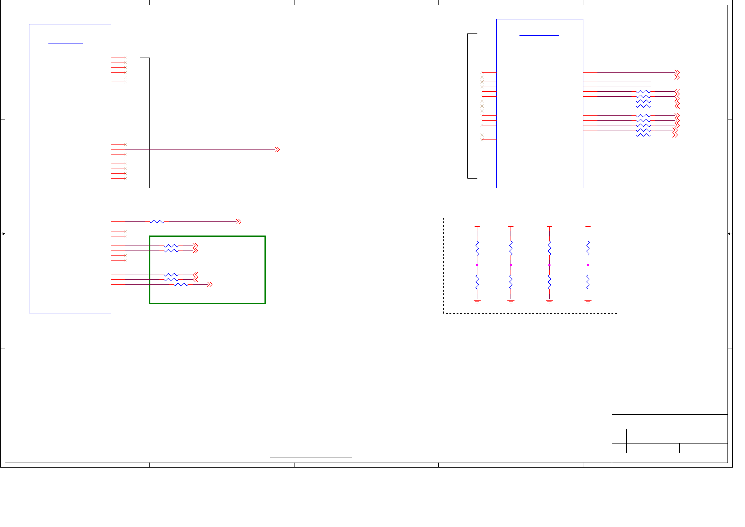
5
4
3
2
1
U1H
U1K
AFE & GPIO
Guest Bus
GADR0
D D
C C
GADR1
GADR2
GADR3
GADR4
GADR5
GDAT0
GDAT1
GDAT2
GDAT3
GDAT4
GDAT5
GDAT6
GDAT7
AC20
V21
AA20
AC21
W21
Y21
AB21
AB22
AB23
AA21
AA22
AA23
Y22
Y23
NAND FLASH INTERFACE
(for intrenal debug usage)
SD_DET 3
Reserved
AC11
AB11
AA11
AA10
AA6
AA5
AB6
AB5
AB8
AA8
AC8
AD8
AE8
AA9
AFE_DIN0
AFE_DIN1
AFE_DIN2
AFE_DIN3
AFE_DIN4
AFE_DIN5
AFE_DIN6
AFE_DIN7
AFE_DIN8
AFE_DIN9
AFE_DIN10
AFE_DIN11
AFE_DINCLK
IF_DVAL
ZR39780_A_6
GPIO_P0
GPIO_P1
GPIO_P2
GPIO_P3
GPIO_P4
GPIO_P5
GPIO_P6
GPIO_P7
GPIO_P20
GPIO_P21
GPIO_P22
GPIO_P23
GPIO_P24
E11
D11
C11
B11
A11
E12
D12
C12
B2
A2
A3
B3
C3
GPIO0
GPIO1
GPIO2
GPIO3
GPIO0 5
GPIO1 12
R41015
R40215
R40915
R40815
R40315
R40715
R40615
R27815
R28315
AUD_SEL0 6
AUD_SEL1 6
SVIDEO_DET 7
AV3_DET 6
COMP_SW1 8
COMP_SW2 8
BL_PWM_CNTRL10
COM1_DET 8
COM2_DET 8
Bootstrap Configuration
R27715
R741 15
1 2
R730 15
SPI_WEN 3
R40415
R40115
R39915
USB_OC 3
AUTO_SW 8
HEADPHONE_PLUG 9
SVIDEO_DET1 7
I2C_SEL/INT_CPU 16
GPIO3
R286
4.75K_NS
R279
4.75K
GPIO2
R287
4.75K_NS
R280
4.75K
GPIO1
R288
4.75K
R281
4.75K_NS
VCC3_3VCC3_3VCC3_3VCC3_3
R282
4.75K_NS
GPIO0
R289
4.75K
GALE
U21
AC22
U22
V22
V23
W23
U23
AC23
W22
AB20
GPIO_P8
GIORD_N
GIOWR_N
GOE_N
GWE_N
GWS_ACK
GCS_N0
GCS_N1
GCS_N2
B B
ZR39780_A_6
A A
Title
Matrix / HD780 Ref. Platform
Size Document
B
780_rev_A1.dsn
Sheet
11 21
GPIO / Guest Bus
Date:
Friday, January 18, 2008
5
4
3
2
Drawn by: S. Nguyen
of
1
Rev
A1
Page 44
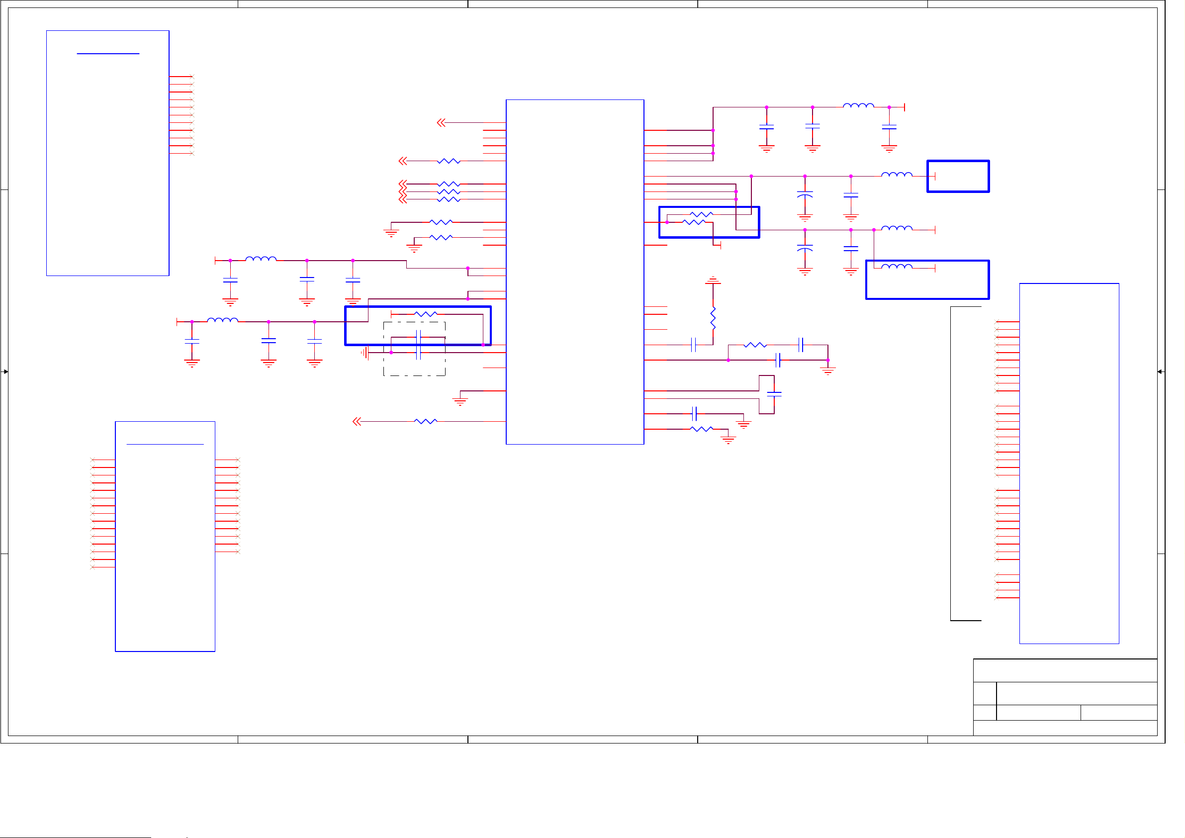
5
Transport I/F
U1D
4
3
2
1
TPDATA7
TPDATA6
TPDATA5
D D
C C
ZR39780_A_6
TPDATA4
TPDATA3
TPDATA2
TPDATA1
TPDATA0
TPVALID
TPFRAME
TPCLK
VCC3_3
No Connect Pins
AA1
NC_AA1
B B
AA25
AA26
AA7
AB10
AB19
AB7
AC19
AC3
AC4
AC5
AD11
AE10
AE11
AE3
NC_AA25
NC_AA26
NC_AA7
NC_AB10
NC_AB19
NC_AB7
NC_AC19
NC_AC3
NC_AC4
NC_AC5
NC_AD11
NC_AE10
NC_AE11
NC_AE3
AB14
AD14
AB13
AC13
AD13
AD12
AC12
AB12
AC14
AC15
AB15
VCC3_3
NC_AF10
NC_AF3
NC_AF9
NC_B25
NC_G6
NC_K22
NC_R23
NC_U1
NC_U24
NC_U6
NC_V25
NC_Y1
NC_Y2
L23
LI0603G121R
C671
0.1uF
U1M
AF10
AF3
AF9
B25
G6
K22
R23
U1
U24
U6
V25
Y1
Y2
L22
LI0603G121R
C320
0.1uF
C239
1.0uF
GPIO111
C235
1.0uF
C240
0.1uF
AUD_AMP_MUTE9
DISPLAY/HV-ON10
USB_PPON3
ADVCC2_1
DVD_STB17
C236
0.1uF
XCLK
3
R971 0 ohm
C237 10uF
C243 10uF
DEMO 4.7UF
R295
0 ohm
12
12
为
U1Q
AC7
AFE_XCLK_TEST
N5
AFE_ATCLK0
P5
AFE_ATCLK1
G7
AFE_CLK
AE7
R40015
R28415
R40515
R29015
R291845R 1%
12
R292845R 1%
12
AFE_TCLK_IN
Y5
AFE_TCLK_OUT
W5
AFE_TEST0
AB9
AFE_TEST1
AC9
AFE_TEST2
L3
LVDSVCRX_REXT
U7
LVDSVCRX_ATST
L4
LVDSVCTX_REXT
AA4
LVDSVCTX_ATST
AB2
LVDSRX_VDD33_0
AB3
LVDSRX_VDD33_1
AA3
LVDSTX_VDD33_0
AB4
LVDSTX_VDD33_1
W6
PGA_LDO
L1
AVDDLDO
M5
VBG
T1
AVSUB
AD7
TRIN_RESET_N
ZR39780_A_6
AVDD_SYNC1
AVDD3_HPLL
AVDD3_SYNC
AVDD3_AFE
AVDD18_HPLL
AVDD18_R
AVDD18_G
AVDD18_B
DVDD18
AFE_CLAMPDAT
AFE1_HSYNC_IN
AFE1_VSYNC_IN
VCOOUT
AFE_VOUT
VFILTOUT
VREFP
VREFN
VCOM
RSET
R2
M1
N1
N2
M2
P2
P1
R1
R973 0 ohm
T2
R972 0 ohm_DNS
M4
AB1
AA2
W4
C241 1.0uF
Y6
L2
W1
W2
C246 470nF
V1
R296 62K
M3
1 2
12
C229
0.1uF
ADVCC2_1
R293
75
R294 3.3K 1%
1 2
C244 3.9nF
C230
1.0uF
C232
1000pF
C522
1000pF
C242 39nF
1 2
12
4.7uF
C245
1 2
LI0603G121R
C233
.01uF
C523
.01uF
DIGITAL VIDEO INTERFACE
reservede for internal
debug
L20
C273
0.1uF
LI0603G121R
LI0603G121R
LI0603G121R_DNS
VCC3_3
L21
L42
L44
VCC1_8_AVDD
ADVCC2_1
VCC1_8_AVDD
E3
E2
E1
F1
D2
D1
C2
C1
B1
A1
F3
F5
F4
F2
G1
G2
G3
G5
G4
H1
H6
H2
H3
H4
H5
K1
K4
K3
K2
J1
J2
J3
J4
J5
BLUE0
BLUE1
BLUE2
BLUE3
BLUE4
BLUE5
BLUE6
BLUE7
BLUE8
BLUE9
GREEN0
GREEN1
GREEN2
GREEN3
GREEN4
GREEN5
GREEN6
GREEN7
GREEN8
GREEN9
RED0
RED1
RED2
RED3
RED4
RED5
RED6
RED7
RED8
RED9
DATACK
HSOUT
VSOUT
OE_FIELD
U1S
A A
ZR39780_A_6
Title
ZR39780_A_6
Matrix / HD780 Ref. Platform
Size Document
B
780_rev_A1.dsn
Sheet
12 21
of
Date:
Friday, January 18, 2008
5
4
3
2
Drawn by: S. Nguyen
1
Rev
A1
Page 45
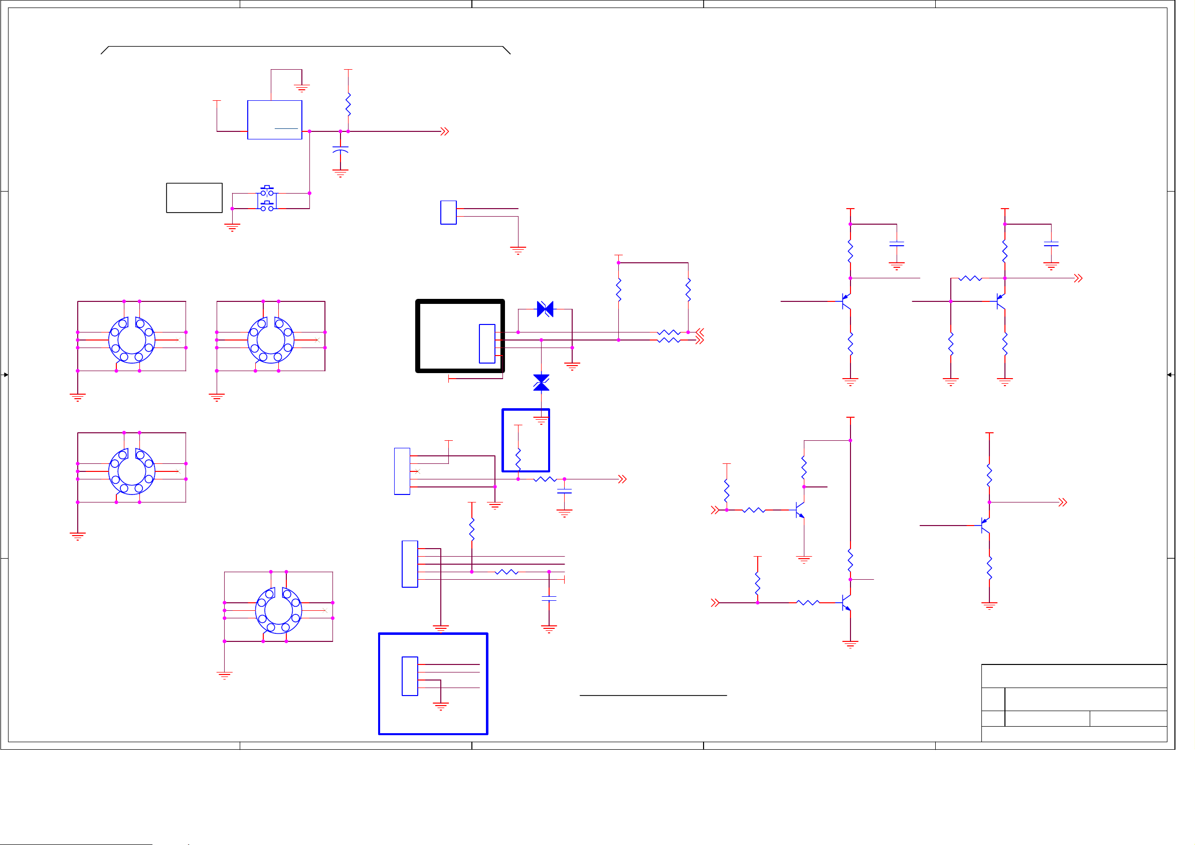
5
4
3
2
1
Reset Circuit
VCC3_3
D D
VCC3_3
Reset
Switch
C C
H2 GEN315R140-8
1
8
2
9 10
3
4
7
6
5
2
9 10
3
1
GND
RESETVCC
U19
AP1701_DNS
SW1
1 2
3 4
button_4pin_DNS
H1 GEN315R140-8
1
8
4
5
R297
1K
23
C247
0.1uF
7
6
TJC3-4A (4pin/2.5mm)
VCC5_0
RESETN 3,16
CNE3
IR_DVD
2
2
1
1
EJTAG2 (2pin/2.0mm)
CNB1
1
1
2
2
3
3
4
4
D89
12
DZ23C10_DNS
12
D90
R302
4.7K
VCC3_3
R304100
R305100
SPDIF OUT
R303
4.7K
UART0TX 3,8
UART0RX 3,8
VCC5_0
IR_DVD
C248
0.1uF
R990 0R
IR
R298
4.7K
23
IR
Q8
1
MMBT3906
R306
0
R991
22K
1
3.3VSB
23
Q9
R299
4.7K_DNS
IR_MCU
MMBT3906_DNS
R307
0_DNS
C249
0.1uF
INFRARED_MCU 16
DZ23C10_DNS
5VSB
IR
R314
220
LED_G
Q12
MMBT3904
2
R300
10K_DNS
R316 100
3.3VSB_MCU
R312
100K
R313 10K
LED_G
LED_R
IR
C252
68PF
KEY 16
C251
10nPF
5VSB
MISC & Connectors
3
3.3VSB
R467
4.7K
1K
LED1_CTL16
LED2_CTL16
R311
3.3VSB
R468
4.7K
R317
R308
220
LED_R
Q10
MMBT3904
1K
H4 GEN315R140-8
1
8
2
B B
A A
9 10
3
4
5
7
6
5
H7 GEN315R140-8
1
8
2
9 10
3
4
7
6
5
4
CNE2
5
4
3
2
1
PH-4A5pin/2.0mm)
CNE1
5
4
3
2
1
EJTAG6 (6pin/2.0mm)
CNE7
4
3
2
1
EJTAG6 (6pin/2.0mm)
5VSB
5
4
3
2
1
5
4
3
2
1
4
3
2
1
KEY_IN
5VSB
LED_G
LED_R
KEY_IN
VCC3_3
R309
4.7K
23
Q11
1
MMBT3906
R315
Title
Size Document
B
Date:
Drawn by: S. Nguyen
IR_760
0
INFRARED_760 3
Matrix / HD780 Ref. Platform
780_rev_A1.dsn
Sheet
13 21
of
Friday, January 18, 2008
1
Rev
A1
Page 46

3.3V Bypass Caps
5
4
3
2
1
1.8V Bypass Caps
VCC3_3
U1R
VCC1_8
Power
C253
D D
0.1uF
VCC3_3
C269
0.1uF
C254
0.1uF
C270
0.1uF
C255
0.1uF
C271
0.1uF
C256
0.1uF
C272
0.1uF
C257
0.1uF
C274
0.1uF
C258
0.1uF
C259
0.1uF
C275
0.1uF
1.0V Bypass Caps
C315
.01uF
C321
1.0uF
HDMI_VDD22
VCC1_0
C292
1.0uF
VCC1_0
C304
1.0uF
C293
1.0uF
C305
1.0uF
C316
1000pF
HDMI_VDD
C322
0.1uF
HDMI_VDD
VCC1_0
C C
B B
A A
VCC1_0
C287
1.0uF
C299
1.0uF
C288
1.0uF
C300
1.0uF
VCC1_8_AVDD
VCC3_3
C289
1.0uF
C301
1.0uF
C290
1.0uF
C302
1.0uF
L28
LI0603G121R
L30
LI0603G121R
C291
1.0uF
C303
1.0uF
C260
1.0uF
C276
1.0uF
C294
1.0uF
C306
1.0uF
C277
0.1uF
C295
1.0uF
C307
1.0uF
C296
1.0uF
C308
1.0uF
VCC1_0
F12
F13
F14
F15
F16
G12
G13
G14
G15
G16
K6
K7
M6
M7
N6
N7
P7
R7
T7
L20
L21
M20
M21
N20
N21
P20
P21
R20
R21
T20
T21
T22
T23
T24
T25
T26
Y11
Y12
Y13
Y14
Y15
Y16
AA12
AA13
AA15
AA16
AA17
AA18
AA19
P6
R6
T6
F6
F7
F8
F9
F10
F11
L6
L7
CORE_VDD0
CORE_VDD1
CORE_VDD2
CORE_VDD3
CORE_VDD4
CORE_VDD5
CORE_VDD6
CORE_VDD7
CORE_VDD8
CORE_VDD9
CORE_VDD10
CORE_VDD11
CORE_VDD12
CORE_VDD13
CORE_VDD14
CORE_VDD15
CORE_VDD16
CORE_VDD17
CORE_VDD18
CORE_VDD19
CORE_VDD20
CORE_VDD21
CORE_VDD22
CORE_VDD23
CORE_VDD24
CORE_VDD25
CORE_VDD26
CORE_VDD27
CORE_VDD28
CORE_VDD29
CORE_VDD30
CORE_VDD31
CORE_VDD32
CORE_VDD33
CORE_VDD34
CORE_VDD35
CORE_VDD36
CORE_VDD37
CORE_VDD38
CORE_VDD39
CORE_VDD40
CORE_VDD41
CORE_VDD42
CORE_VDD43
CORE_VDD44
CORE_VDD45
CORE_VDD46
CORE_VDD47
CORE_VDD48
CORE_VDD49
CORE_VDD50
CORE_VDD18_0
CORE_VDD18_1
CORE_VDD18_2
HDMI_VDD_0
HDMI_VDD_1
HDMI_VDD_2
HDMI_VDD_3
HDMI_VDD_4
HDMI_VDD_5
ZR39780_A_6
IOVDD0
IOVDD1
IOVDD2
IOVDD3
IOVDD4
IOVDD5
IOVDD6
IOVDD7
IOVDD8
IOVDD9
IOVDD10
IOVDD11
IOVDD12
IOVDD13
IOVDD14
IOVDD15
IOVDD16
IOVDD17
IOVDD18
IOVDD19
IOVDD20
IOVDD_I
MVDD0
MVDD1
MVDD2
MVDD3
MVDD4
MVDD5
MVDD6
MVDD7
MVDD8
MVDD9
MVDD10
MVDD11
MVDD12
MVDD13
MVDD14
MVDD15
MVDD16
MVDD17
MVDD18
MVDD19
MVDD20
MVDD21
MVDD22
MVDD23
USB_VDD1
USB_VDD33
PLL_VDD
DAC_VDD
LDI_VDD1
LDI_VDD0
G8
G9
G10
G11
H7
H8
J6
J7
U20
V7
V20
W7
W20
Y7
Y8
Y9
Y10
Y17
Y18
Y19
Y20
V6
E19
E20
E21
E22
F17
F18
F19
F20
F21
F22
G17
G18
G19
G20
G21
G22
H20
H21
H22
J20
J21
J22
K20
K21
E6
E4
V26
AC26
AB18
AC18
VCC3_3
VCC1_8
C654
0.1uF
VCC1_8
C278
0.1uF
C309
0.1uF
C312
0.1uF
C317
0.1uF
C323
0.1uF
C655
0.1uF
C279
0.1uF
1000pF
C297
1.0uF
1.0uF
1.0uF
1.0uF
1000pF
C310
C313
C318
C324
C656
0.1uF
C280
0.1uF
C285
C657
0.1uF
C281
0.1uF
C286
.01uF
C298
.01uF
LI0603G121R
LI0603G121R
LI0603G121R
LI0603G121R
C658
0.1uF
C282
0.1uF
LI0603G121R
L26
C311
0.1uF
L27
C314
0.1uF
L29
C319
0.1uF
L31
C325
0.1uF
C659
0.1uF
C651
0.1uF
LI0603G121R
L25
VCC3_3
VCC3_3
VCC3_3
VCC3_3
L24
C660
0.1uF
C652
0.1uF
VCC1_0
C661
0.1uF
C653
0.1uF
VCC3_3
Title
Matrix / HD780 Ref. Platform
Size Document
B
780_rev_A1.dsn
Sheet
14 21
HD780 Power
5
4
3
2
Date:
Friday, January 18, 2008
Drawn by: S. Nguyen
of
1
Rev
A1
Page 47

5
VCC1_8
VCC3_3
VCC1_0
VCC1_0
C669
1.0uF
C673
1.0uF
C679
1.0uF
C686
0.1uF
D D
C705
1.0uF
C C
B B
C668
1.0uF
C685
0.1uF
C678
1.0uF
C667
0.1uF
C666
0.1uF
C672
1.0uF
C677
1.0uF
C684
0.1uF
C665
0.1uF
C664
0.1uF
C670
0.1uF
C676
1.0uF
C683
0.1uF
C663
0.1uF
C682
0.1uF
C675
1.0uF
C662
33uF
+
C346
0.1uF
C342
33uF
C674
1.0uF
+
C681
0.1uF
+
C327
1000uF
+
C343
33uF
4
U1N
3
2
1
Bulk Bypass Caps
Ground
VCC3_3VCC1_0 VCC1_8
C694
10uF
N17
GND47
N16
GND46
N15
GND45
N14
GND44
N13
GND43
N12
GND42
N11
GND41
N10
GND40
N9
GND39
M18
GND38
M17
GND37
M16
GND36
M15
GND35
M14
GND34
M13
GND33
M12
GND32
M11
GND31
M10
GND30
M9
GND29
L18
GND28
L17
GND27
L16
GND26
L15
GND25
L14
GND24
L13
GND23
L12
GND22
L11
GND21
L10
GND20
L9
GND19
K18
GND18
K17
GND17
K16
GND16
K15
GND15
K14
GND14
K13
GND13
K12
GND12
K11
GND11
K10
GND10
K9
GND9
J18
GND8
J17
GND7
J16
GND6
J15
GND5
J14
GND4
J13
GND3
J12
GND2
J11
GND1
J10
GND0
B24 V5
GND99 GND106
N3
GND100
N4
GND101
P3
GND102
GND49GND48
GND50
GND51
GND52
GND53
GND54
GND55
GND56
GND57
GND58
GND59
GND60
GND61
GND62
GND63
GND64
GND65
GND66
GND67
GND68
GND69
GND70
GND71
GND72
GND73
GND74
GND75
GND76
GND77
GND78
GND79
GND80
GND81
GND82
GND83
GND84
GND85
GND86
GND87
GND88
GND89
GND90
GND91
GND92
GND93
GND94
GND95
GND96
GND97
GND98
GND105
GND104
GND103
P9N18
P10
P11
P12
P13
P14
P15
P16
P17
P18
R9
R10
R11
R12
R13
R14
R15
R16
R17
R18
T9
T10
T11
T12
T13
T14
T15
T16
T17
T18
U9
U10
U11
U12
U13
U14
U15
U16
U17
U18
V9
V10
V11
V12
V13
V14
V15
V16
V17
V18
U5
R25
P4
C687
10uF
C696
10uF
C688
10uF
C697
10uF
C689
10uF
C698
10uF
C690
10uF
VCC1_8VCC1_0
C699
10uF
2 caps on side, 1 cap near DDR21 cap per side 1 cap per side
C691
10uF
C700
10uF
C692
10uF
C701
10uF
ZR39780_A_6
A A
Title
Matrix / HD780 Ref. Platform
Size Document
B
780_rev_A1.dsn
Sheet
15 21
HD780 Ground
5
4
3
2
Date:
Friday, January 18, 2008
Drawn by: S. Nguyen
of
1
Rev
A1
Page 48

5
4
3
2
1
5VSB
C708
D D
10UF/16V
C C
C709
+
0.1uF
8
MCU_I2C2DATA
22
MCU_I2C2CLK
22
U44 UR133L-3.3V-C
2
Vin Vout
GND
1
VGA_UART_ON/OFF
MCU_I2C2DATA
MCU_I2C2CLK
3.3VSB_MCU
3
3.3VSB_MCU
R489
4.7K
4.7K
R802
L32 10uH
C511
+
10UF/16V
4.7K
R803
3.3VSB_MCU
12
U20
AMP_SD9
LCD_ON10
ADU_PWR_CTRL18
LCD_PWR_SW17
MCU_RST_IN
INFRARED_MCU13
POWER_ON17
RESETN3,13,22
R334 100
R335 100
R329 100
R332 100
R331 100
R327 100
R325 100
R413 100
R336
R323 100
100
XTAL1
XTAL2
1
DAC0/P2.0
2
P2.1
3
KBI0/CMP2/P0.0
4
P1.7
5
P1.6
6
RST/P1.5
7
VSS
8
XTAL1/P3.1
9
CLKOUT/XTAL2/P3.0
10
INT1/P1.4
11
SDA/INT0/P1.3
12
SCL/T0/P1.2
13
MOSI/P2.2
14 15
MISO/P2.3 P2.4/SS
P89LPC933
P0.1/CIN2B/KBI1/AD10
P0.2/CIN2A/KBI2/AD11
P0.3/CIN1B/KBI3/AD12
P0.4/CIN1A/KBI4/DAC1/AD13
P0.5/CMPREF/KBI5
P0.6/CMP1/KBI6
P2.7
P2.6
VDD
P0.7/T1/KBI7
P1.0/TXD
P1.1/RXD
P2.5/SPICLK
28
27
26
9
25
24
23
22
21
20
19
18
17
16
VCC5_0
3.8V
R333 100
R602 100
R603 100
R339 100
R338 100
R330 100
R604 100
R322 100
R319 100
R328 100
R326 100
R318
1K
R320
10K
PWR_SW_DVD 17
AUD_AMP_MUTE_MCU
PDA
PCL
UART1RX
UART1TX
LED_R
LED_B
KEY 13
UC_CEC_MCU
RESETN_AUD_HDMI 9 22
LED1_CTL 13
LED2_CTL 13
I2C_SEL/INT
22
3.3VSB
R970
4.7K
I2C_SEL/INT 22
VDD
D138
1N4148
RGB_VSYNC
3.3VSB_MCU
C512
0.1uF
8
U37
5
1
GND
RESETVCC
AP1701_DNS
1
2
3 4
23
Q35
S1
G1
D2 S2
UM6K1N
D1
G2
R600
1K
C576
0.01uF
6
5
MCU_RST_IN
R609
100K
C389
22pF
VCC3_3
MCU_I2C2CLK
MCU_I2C2DATA
3.3VSB
XTAL1
R993 1M
Y3
1 2
12MHz
XTAL2
R601
330
C390
22pF
4
I2C2CLK
I2C2DATA
R790 0_DNS
R791 0_DNS
R977 0_DNS
PDA
MCU_I2C2CLK
MCU_I2C2DATA
I2C_SEL/INT_CPUI2C_SEL/INT
5
CON25
1
2345
JK_2.5
1
2
34
MCU_RST_IN
PCL
3
2 3
Q40 AO3401
1
R805
4.7k
3.3VSB
VDD
C575
1k R
VCC3_3
R806
4.7K
I2C_SEL/INT_CPUI2C_SEL/INT
CON33
1
2
3
4
TJC3-4A_DNS
I2C_SEL/INT_CPU11
5VSB
2
R419 100
R418 100
VCC3_3
R342
4.7K
R343
4.7K
UART1RX
UART1TX
UART1RX 3
UART1TX 3
MCU
Title
Haier_HD780 Platform
Size Document
B
Haier_780_V2.0.dsn
Sheet
16 21
of
Date:
Friday, January 18, 2008
Drawn by: S. Nguyen
1
Rev
2.0
3.3VSB_MCU
B B
I2C2DATA
A A
3
3
I2C2CLK
I2C2DATA
I2C2CLK
Page 49

5
4
3
U42
2
1
1
R751 100k
VCC12_0
C612
D D
C393
0.1uF
4.7K
VCC12_0
C398
0.1uF
1 2
3.3VSB
Panel_power
C421
0.1uF
5VSB
R349
4.7K
VCC12_0
POWER_ON 16
C412
470uF/16V
C413
+
0.1uF
1 2
VCC12_0
C429
+
470uF/16V_DNS
4.7k
R359
VCC12_0
C401
470uF/16V
2 3
5 6
19
18
17
4
C430
0.1uF_DNS
1 2
R380
4.7k
VCC6_5
+
U23
IN SW
EN FB
TH_GND
TH_GND
TH_GND
GND
TH_GND
16
2 3
5 6
19
18
17
4
R488 1.5/2W_15mm_DNS
CNA1
7
6
5
4
3
2
1
TJC3-7A(7pin/2.5mm)
C C
LVDS_VD Panel_power
VCC3_3
R358
R361
4.7K
R364
LCD_PWR_SW16
10K
B B
VCC3_3
R376
4.7K
10K
PWR_SW_DVD16
A A
R381
1
4.7K
R362 22K
Q15
1
MMBT3904
2 3
VCC5_DVD_IN VCC5_DVD
CTRL_DVD
R373
4.7K
R379
22K
Q17
MMBT3904
2 3
+
R487 0
100R/0.25W_15mm
2 3
Q27 AO3401
CTRL_LVDS
C422
+
220uF/16V_DNS
Panel ON/OFF Control
2 3
Q26 AO3401
1
C427
0.1uF
1
C437
220uF/16V_DNS
12
12
R987
LVDS_VD
12
MMBT3904
R354 0
R355 0
12V LVDS POWER IS FOR LG LCD.
VCC12_0
1
1
C423
1uF
VCC5_DVD_IN
VCC5_DVD_IN
R372
10K
R375
CTRL_DVD
1K
Q16
MMBT3904
2 3
FOR INNER DVD POWER
MMBT3904
2 3
R356
10K
R360
1K
Q14
1
2
3
4
C432
1uF_DNS
R382
33K
LVDS_VD
CTRL_LVDS
U25
D1
S1
D2
S2
D3
S3
D4
G
FDS9435A_DNS
C431
0.1uF
C392
100uF/16V
5VSB
Q13
2 3
1
2
3
4
FDS9435A_DNS
C418
1uF_DNS
R366
33K
8
7
6
5
C435
220uF/16V
U24
S1
S2
S3
G
+
R348
1K
0.1uF
D1
D2
D3
D4
1
VCC12_0
8
7
6
5
C416
VCC5_DVD
1 2
12
C397
47uF/16V
R351
C420
220uF/16V
C436
0.1uF
+
0.1uF
1 2
R344 100k
R345 100k_DNS
C402
+
47uF/16V
1 2
1
BST
SC4519
COMPSYNC
TH_GND
TH_GND
TH_GND
TH_GND
TH_GND
TH_GND
13
14
15
U26
1
IN SW
EN FB
SC4519_DNS
TH_GND
TH_GND
TH_GND
GND
TH_GND
TH_GND
15
16
C611 Option
R752 3.9k
C396 Option
R346 3.9k
C403
0.1uF
78
10
C419
11
180pF
12
9
TH_GND
BST
COMPSYNC
TH_GND
TH_GND
TH_GND
TH_GND
TH_GND
TH_GND
13
14
12
C613
Option
78
10
11
12
9
C404
Option
C439
180pF
1 2
12
R365
3.3k
FB
2
AP1513_DNS
EN
3
OCSET
4 5
VCC Output
C614
0.1uF
1 2
U22
1
FB
2
EN
3
OCSET
4 5
VCC Output
C405
0.1uF
1 2
1 2
D94
1N4148
C410
0.22uF
L35 10uH/3A
L5-9
R385
3.3k
C417
3.3nF
31.6K_1%
D95
1N5822
C426
0.22u
L37 10uH/3A_DNS
L5-9
C438
3.3nF
D97
1N5822_DNS
AP1530
R357
R485
R363
1N4148
VSS
VSS
Output
0
10k_1%
D96
VSS
VSS
Output
+
470uF/16V
R377
31.6K_1%
R383
10k_1%
8
7
6
8
7
6
C411
+
10uF/16V
32PDP_5VIN
C428
+
470uF/16V_DNS
CNA3
D134
1N5822_DNS
D91
1N5822
C414
VCC6_5
C433
+
10uF/16V_DNS
32PDP_5VIN
4
3
2
1
L43 33uH/2A_DNS
L5-9
L33 22uH/3A
L4.5-9
C415
0.1uF
1 2
R368
R369 0_DNS
R370
12
0.1/1W_05_DNS
C434
0.1uF_DNS
1 2
C615
Option
C407
Option
VCC6_5
0_DNS
R371 0
R374 0_DNS
R378 0_DNS
R753
1.27K_1%
1 2
R754
1.02K_1%
R347
909R_1%
1 2
R350
2.49K_1%
32PDP_5VIN
PH05A(5pin/2.0mm)_DNS
VCC5_DVD_IN
Power & Ground 3
Vout=0.8*(1+R753/R754);
R754=0.7K~5K
Vout=0.8*(1+R347/R350);
R350=0.7K~5K
C11
+
+
470uF/16V
CNA4
470uF/16V
5
4
3
2
1
LVDS_VD
VCC1_8
1 2
C355
C12
+
33uF/16V
5V LVDS POWER IS
FOR SUMSUNG/AU/CMO
LCD
C616
0.1uF
VCC1_0
1 2
C409
0.1uF
1 2
C424
0.1uF
+
1.8V - 2A (2.8A MAX)
6.5V - 1.5A (5A MAX)
"Power LED"
LED_DNS
D92
D93
LED_DNS
VCC12_0
C425
100uF/16V
1 2
R352
12
R353 330
12
VCC3_3
C524
0.1uF
R367
4.7K
+
330
VCC5_DVD
C525
100uF/16V
VCC6_5
5VSB
DVD_STB 12
Title
TJC3-3A(3pin/2.5mm)_DNS
5
4
3
2
Matrix / HD780 Ref. Platform
Size Document
C
780_rev_A1.dsn
Sheet
17 21
Friday, January 18, 2008
Date:
Drawn by: S. Nguyen
1
of
Rev
A1
Page 50

5
4
3
2
1
VCC6_5
VCC6_5
D D
VCC6_5
C C
VCC12_0 VCC8_0
VCC6_5
B B
1 2
C463
0.1uF
R386 0
C459
0.1uF
+
100uF/16V
+
C464
VCC5_0
U28 AP1084E18
C460
470uF/16V
U29 LM7808
1
VIN
VCC6_5
23
OUTIN
GND TAB
1 4
R484
100R
TAB
3
VOUT
TAB
GND
2
U30 AP1117E5_DNS
23
OUTIN
R483
220_1%
C465
0.1uF
1 2
R387 0_DNS
+
C462
470uF/16V
+
C466
100uF/16V
VCC1_8
C461
0.1uF
VCC5_TUNER
5VSB
C578
0.1uF
VCC8_0
L39
10uH
VCC5_0
C448
+
22uF/16V
+
C471
0.1uF
U27 AP1084E33
C579
100uF/16V
23
OUTIN
GND TAB
1 4
U38 AP1117E33
OUTIN
GND TAB
1 4
+
C472
10uF/16V
C449
+
100uF/16V
23
C585
0.1uF
U31 AP1117E5
OUTIN
GND TAB
1 4
FB12 150_Ohm_2A
1 2
C450
0.1uF
3.3VSB
+
C586
100uF/16V
23
C473
0.1uF
+
VCC3_3
ADU_PWR_CTRL8
VCC5_TUNER
C474
100uF/16V
3.3VSB VCC3_AUD
2 3
Q38 AO3401
1
VCC1_8_AUD1.8VSB
2 3
Q39 AO3401
1
R804
4.7k
3.3VSB
VCC1_8_AVDD
1 2
FB28
150_Ohm_2A
C467
0.1uF
3.3VSB
C475
0.1uF
A A
+
C476
+
100uF/16V
C468
10uF/16V_DNS
U32 AP1117E18
1 4
1 4
OUTIN
GND TAB
GND TAB
23
C477
0.1uF
C469
0.1uF
+
+
C470
100uF/16V
1.8VSB
C478
100uF/16V
Power & Ground 3
VCC5_0
C518
0.1uF
+
U35 AP1117_ADJ
C519
10uF
OUTIN
GND TAB
1 4
R431 121_1%
R430
82_1%
ADVCC2_1
23
+
C520
100uF/16V
C521
0.1uF
Vout=1.25V*(1+Rdown/Rup)
Title
Matrix / HD780 Ref. Platform
Size Document
B
780_rev_A1.dsn
Sheet
18 21
of
Date:
Friday, January 18, 2008
5
4
3
2
Drawn by: S. Nguyen
1
Rev
A1
Page 51

5
4
3
2
1
U2 Bypass Caps
VCC1_8
D D
C C
C479
0.1uF
VCC1_8
C485
0.1uF
C480
0.1uF
BP2 BP3
C486
0.1uF
BP9 BP10 BP11BP7 BP8 BP12
C481
0.1uF
C487
0.1uF
C482
0.1uF
C488
0.1uF
C483
0.1uF
BP6BP4 BP5BP1
C489
0.1uF
C484
0.1uF
C490
0.1uF
VCC1_8
U33B
J1
A1 A3
E1 E3
J9
C1
C3
C7
C9
G1
G3
G7
G9
A2
E2
DDR II
VDDL
VDD VSS
VDD VSS
VDD
VDDQ
VDDQ
VDDQ
VDDQ
VDDQ
VDDQ
VDDQ
VDDQ
NC1
NC2
K4T51163QC-2CE7_1
VSSDL
VSS
VSSVDD
VSSVDD
VSSQVDDQ
VSSQ
VSSQ
VSSQ
VSSQ
VSSQVDDQ
VSSQ
VSSQ
VSSQ
VSSQ
NC4
NC5
NC6
J7
J3
N1M9
P9R1
A7A9
B2
B8
D2
D8
E7E9
F2
F8
H2
H8
R3
R7
R8
Option:
U3 Bypass Caps
VCC1_8
C491
0.1uF
VCC1_8
B B
C497
0.1uF
C492
0.1uF
BP2 BP3
C498
0.1uF
C493
0.1uF
C499
0.1uF
BP9 BP10 BP11BP7 BP8 BP12
C494
0.1uF
C500
0.1uF
C495
0.1uF
BP6BP4 BP5BP1
C501
0.1uF
C496
0.1uF
C502
0.1uF
VCC1_8
U34B
J1
A1 A3
E1 E3
J9
C1
C3
C7
C9
G1
G3
G7
G9
A2
E2
DDR II
VDDL
VDD VSS
VDD VSS
VDD
VDDQ
VDDQ
VDDQ
VDDQ
VDDQ
VDDQ
VDDQ
VDDQ
NC1
NC2
VSSDL
VSS
VSSVDD
VSSVDD
VSSQVDDQ
VSSQ
VSSQ
VSSQ
VSSQ
VSSQVDDQ
VSSQ
VSSQ
VSSQ
VSSQ
NC4
NC5
NC6
J7
J3
N1M9
P9R1
A7A9
B2
B8
D2
D8
E7E9
F2
F8
H2
H8
R3
R7
R8
Second DDR2 could be reduced
if for ZR770 implementation
only one DDR2 will be
needed.
K4T51163QC-2CE7_1/*NC OPTION
A A
DDR2 Power/Gnd
Title
Matrix / HD780 Ref. Platform
Size Document
B
780_rev_A1.dsn
Sheet
19 21
of
Date:
Friday, January 18, 2008
5
4
3
2
Drawn by: S. Nguyen
1
Rev
A1
Page 52

5
4
3
2
1
GPIO Pin Table
D D
Signal
FP_CHFP_CH+
FP_VOLFP_VOL+
ZR39760 GPIO #
07
06
31
30
FP_MENU 26
FP_VIN_SW 27
FP_SEL 28
Function
Tuner control
Tuner control
VOL control
VOL contol
MENU set
Video IN select (FP)
GUI ENTER
Note
Active low
Active low
Active low
Active low
Active low
Active low
Active low
Setting
0000
0001
0010
0011
Boot Options
Boot from SPI flash, fall back to UART0
Boot from UART0
Boot from SPI flash, fall back to UART1
Boot from UART1
Perform ROM Checksum01XX
36 CVBS -Y/C Video IN Recognition 1=CVBS; 0 = Y/CVideo_Input_Select
04
Enable signal for 12V supplyLCD_PWR_SW
05 LCD backlight on/off controlLCD_ON
C C
SD card CSSD_CSN 34 Act i v e lo w
SD card detectSD_DET 62 Acti v e l o w
33 HDMI HPD RecognitionGPIO_HPD Act i v e hi g h
Active high
Active high
1111
1110
1010
1011
1100
Boot from 8 bit NAND flash
Boot from 16 bit NAND flash
Boot from SPI flash
63 Back light voltage controlBL_BR_CNTRL PWM type
Video IN select VID_IN_SEL 55
Audio PWR Amp MUTEAUD_AMP_MUTE 47 Acti v e l o w
Audio IC's resetAUD_RESETN 48 Ac t i v e low
Tuner PWR switchTU_5V_SW 42 0 = OFF; 1 = ON
B B
A A
Title
Matrix / HD780 Ref. Platform
Size Document
B
GPOIs Table
5
4
3
2
780_rev_A1.dsn
Sheet
21 21
Date:
Friday, January 18, 2008
Drawn by: S. Nguyen
Rev
of
1
A1
Page 53

Page 54
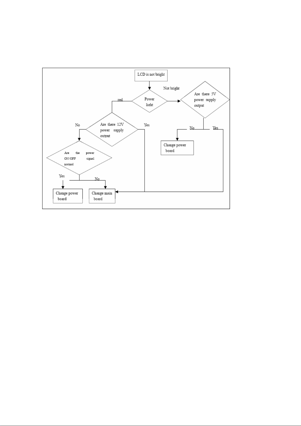
10. TROUBLE SHOOTING GUIDE
10.1. Simple check
10.1.1 LCD is not bright
10.1.2 No picture
33
Page 55

First, check cables which connect with PSUˈthen check as follows
1) Check input voltage
voltage: +5VSBĺPOWER ON(5V) ĺ+12Vĺ5V
connector: CN4(P1) ĺ CN4(P13) ĺCN5(P1,P2,P3) ĺCN4(P2,P3,P4,P5) ĺCN4(P12) ĺCON4(P14)
2)Check output voltage
voltage: Vblon ĺ+5VĺVipwm
connector: CN4(P12) ĺJ28(P26-P30) ĺCON4(P14)
CN4 CN5
On/Off Control
Voltage
Control Voltage
ON - 2.0 - 5.0 V
OFF
MAX 3.0 3.15 3.3 V Maximun duty ratio Internal PWM
MIN
VBLON
- 0 - 0.8 V
VIPWM VSEL=L
0 - V Minimum duty ratio
34
Page 56
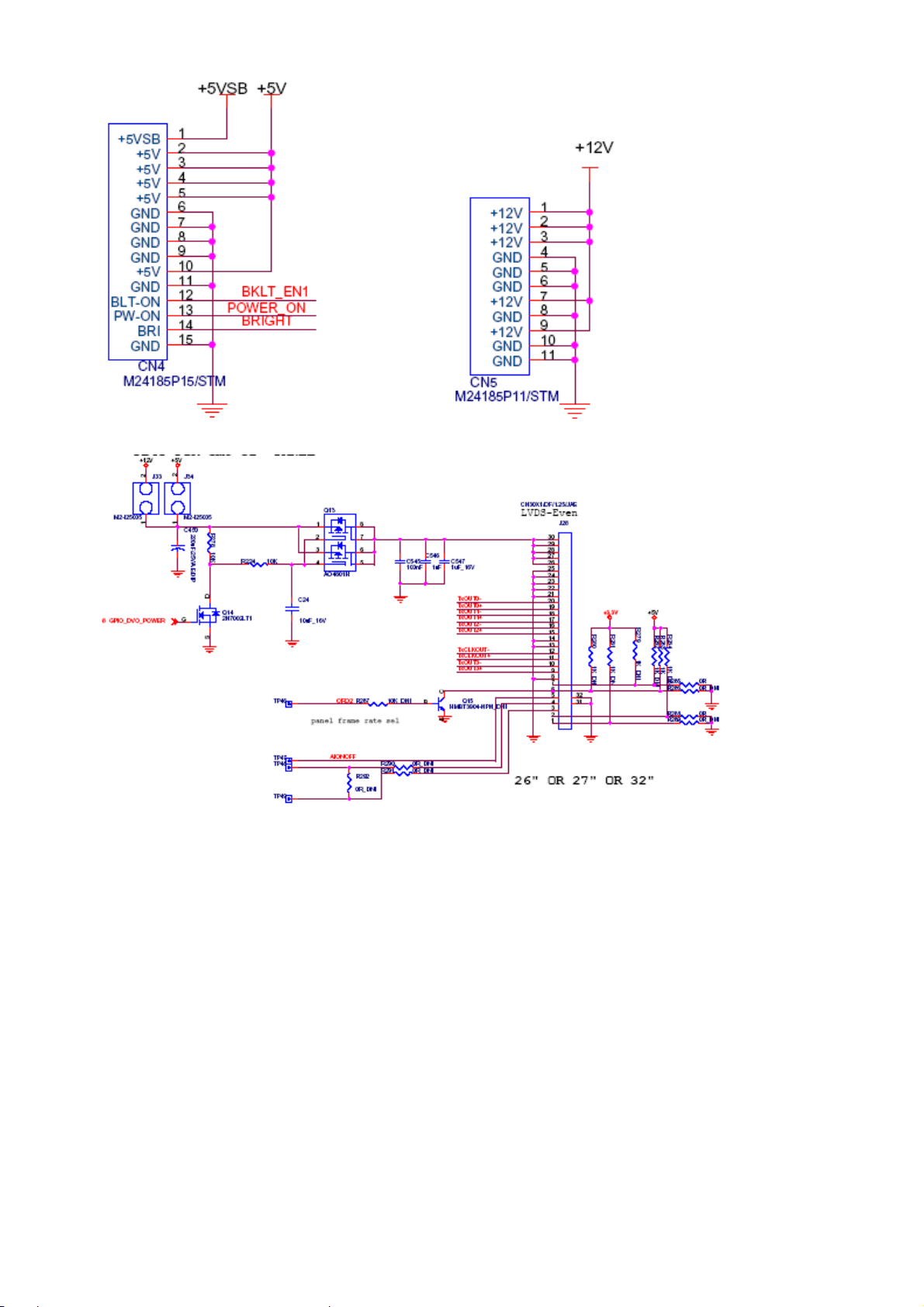
CN4 CN5
10.1.3 No sound
35
Page 57

No sound
Y
N
Y
1st pin of
CN20 is 18V?
Is 45th of
U29 low?
Y
IS there input
of 2ed pin of
U29?
Change power
board
N
Change U29
N
Change main board
Y
Is there output
st
of 21
and 39
pins of u29
Y
Change speaker
N
th
Change U29
36
Page 58

Firstˈcheck cables which connect with PSUˈthen check as follows
1) Check input voltage as NO picture
2) Check speaker output
First, check speaker anode (+) and cathode (-),confirm speaker short or not. If short , replace speaker.
Second, check CN2, CN3 with oscillograph, confirm wave output or not.
Connector: CN2, CN3
10.2 PSU failure check
State: No power
First, check cables which connect with PSU, then check as follows
1) Check PSU input voltage˄AC input˅
voltage : 120V
connector:CON1˄P1,P5˅
2˅Check PSU output voltage orderly˖
voltage :+5V(Stand-By)ĺON˄5.0V˅ĺ+24V ,+12V
connector:CON4˄3˅ĺCON4˄1˅ĺCON4˄6,7˅,CON2˄1-4˅
State˖No sound
10.3 Panel failure
37
Page 59

Failure Mode
Part Name Description Phenomena Failure cause
TCP
V B/D
V
Dim
V L/D
H B/D
H
Dim
H L/D
Vertical
bar
Virtal gray
line
Vertical
color
line(light or
dark
forever)
Horizontal
bar
Horizontal
gary line
Horizontal
line(light or
dark
forever)
Block Defect :TCP cracking or cracking
Dim or L/D :TCP Sunken
:TCP lead cracking
:ACF bonding short
:Awful environment and something electric
enter into
LCD
:Mis-align between TCP and Panel
:Panel failure
:TCP failure
Failure Mode
Part Name Description Phenomena Failure cause
Bright dot dark
dot in panel
Bladder in
Polarizer
Polarizer
Scratch
Eyewinker
inside Polarizer
Incoming Inspection Standard
Bladder between Polarizer and top glass
Tine or rigidity arose
Eyewinker inside Polarizer
Panel or
Polarlzer
Dot Defect
Polarizer
Bubble
Polarizer
Scratch
F/M inside
Polarizer
Circuit
Abnormal
Display
Abnormal
Display
1.Chip lose action
2.IC Abort or jointing bad
38
Page 60

3.Panel and VSC connect bad
Flashing
Bright and dark
display
alternately
Failure Mode
Part Name Description Phenomena Failure cause
Circuit
White
Screen
B/L normal,
only white
screen display
Maybe caused by surge current and EDS
Black
Screen
B/L normal,
only Black
screen display
FIIcker Crosstalk LCD Vcom imbalance
Abnormal
Color
Abnormal
Color
Only color
abnormal
Only color
abnormal
Capacitance improper bring crosstalk
inside LCD panel
1.Chip lose action
2. IC short or joint bad
3.Panel and VSC connect bad
Failure Mode
Part Name Description Phenomena Failure cause
Mechanlcal
Nolse
Ripple
When turn
panel,appear
cacophony
Connectric
circle
B/L off B/L lose action
*Connect badness between wire and
39
Caused by Mechanica noise of backlight
unit
Causeed by between mechanism and
Panel
electrode
Page 61

B/L dark
B/L brightness
darker than
normal
*Connect badness
Short between wire and electrode
B/L wire
damaged
B/L wire
open
B/L shut
down
B/L wire
damaged
Without
backlight
B/L shutdown in
sometime
Operation abnormal or systemic noise
Operation abnormal or systemic noise
Short between lamp housing and wire,
Because consume power too much
F/M in
F/M
B/L ,white, back
Rotundity or
F/M in B/L unit
wire like
Failure Mode
Part Name Description Phenomena Failure cause
Brightness at
Light
leakage
bottom of LCM
brighter than
B/L unit badness
normal
Mechanlcal
or B/L
Uniformity
Mount hole
B/L brightness
asymmetric
Lack screw or
screw damage
Sheet in B/L unit is uneven
*Lack screw
Screw damage
40
 Loading...