

Page 1
18.5&21.5&23.6 LCD TV Haier LE19C1320&LE22/24C1380
Service
Service
Service
31~75 KHz
Description Page Description Page
Table of Contents.......……....................................…........1
Important Safety Notice.......................................……......2
Revision List…………………………………………………3
1. General Specification.................................………........4
2. Operating Instructions…………………….……...….......6
2.1 The Use of Remote Control…….…………...…….......6
2.2 To Use the Menus…...………………….….………......7
2.3 Front Panel Control Knobs……………….………......13
2.4 How to Connect…….…………………….…..…….....14
3. Input/Output Specification…………....................…....15
4. Mechanical Instructions…………………….................19
5. Repair Flow Chart ………………………………………24
6. PCB Layout …………...………………………………...31
6.1 Main Board………..…………………...…….….......31
ANY PERSON ATTEMPTING TO SERVICE THIS CHASSIS MUST FAMILIARIZE HIMSELF WITH THE CHASSIS
TABLE OF CONTENTS
6.2 Power Board…..…………..………….…..…….......33
6.3 Key Board………………………..……..……….......42
6.4 IR Board…………………………..……….…….......42
7. Adjustment..............................................................43
7.1 ADC Adjustment……………………..……...………43
7.2 FW Upgrade.………………………………...………44
7.3 The Writing VGA & HDMI EDID….………...………48
8. Block Diagram.…….................................................53
9. Wiring Diagram.……...............................................54
10. Schematic Diagram………..……..………………...57
10.1 Main Board…………….…………………...….......57
10.2 Power Board………..…....…………...……….......67
10.3 Key Board……………….………….………….......73
10.4 IR Board……………………………….……….......74
SAFETY NOTICE
Horizontal Frequency
AND BE AWARE OF THE NECESSARY SAFETY PRECAUTIONS TO BE USED WHEN SERVICING
ELECTRONIC EQUIPMENT CONTAINING HIGH VOLTAGES.
CAUTION: USE A SEPARATE ISOLATION TRANSFOMER FOR THIS UNIT WHEN SERVICING
1
Page 2

Important Safety Notice
Proper service and repair is important to the safe, reliable operation of all Haier Company Equipment. The service
procedures recommended by Haier and described in this service manual are effective methods of performing
service operations. Some of these service operations require the use of tools specially designed for the purpose.
The special tools should be used when and as recommended.
It is important to note that this manual contains various CAUTIONS and NOTICES which should be carefully read in
order to minimize the risk of personal injury to service personnel. The possibility exists that improper service
methods may damage the equipment. It is also important to understand that these CAUTIONS and NOTICES ARE
NOT EXHAUSTIVE. Haier could not possibly know, evaluate and advise the service trade of all conceivable ways in
which service might be done or of the possible hazardous consequences of each way. Consequently, Haier has not
undertaken any such broad evaluation. Accordingly, a servicer who uses a service procedure or tool which is not
recommended by Haier must first satisfy himself thoroughly that neither his safety nor the safe operation of the
equipment will be jeopardized by the service method selected.
Hereafter throughout this manual, Haier Company will be referred to as Haier.
WARNING
Use of substitute replacement parts, which do not have the same, specified safety characteristics might create
shock, fire, or other hazards.
Under no circumstances should the original design be modified or altered without written permission from Haier.
Haier assumes no liability, express or implied, arising out of any unauthorized modification of design.
Servicer assumes all liability.
FOR PRODUCTS CONTAINING LASER:
DANGER-Invisible laser radiations when open AVOID DIRECT EXPOSURE TO BEAM.
CAUTION-Use of controls or adjustments or performance of procedures other than those specified herein may
result in hazardous radiation exposure.
CAUTION -The use of optical instruments with this product will increase eye hazard.
TO ENSURE THE CONTINUED RELIABILITY OF THIS PRODUCT, USE ONLY ORIGINAL MANUFACTURER'S
REPLACEMENT PARTS, WHICH ARE LISTED WITH THEIR PART NUMBERS IN THE PARTS LIST SECTION OF
THIS SERVICE MANUAL.
Take care during handling the LCD module with backlight unit.
-Must mount the module using mounting holes arranged in four corners.
-Do not press on the panel, edge of the frame strongly or electric shock as this will result in damage to the screen.
-Do not scratch or press on the panel with any sharp objects, such as pencil or pen as this may result in damage to
the panel.
-Protect the module from the ESD as it may damage the electronic circuit (C-MOS).
-Make certain that treatment person’s body is grounded through wristband.
-Do not leave the module in high temperature and in areas of high humidity for a long time.
-Avoid contact with water as it may a short circuit within the module.
-If the surface of panel becomes dirty, please wipe it off with a soft material. (Cleaning with a dirty or rough cloth may
damage the panel.)
2
Page 3

Revision List
Version Release Date Revision Instructions Customer Model Model
Jan.18,2011
A00
Feb.28,2011
Initial release
LE24C1380 E2CB6ZNKWNH6NN
LE19C1320 E19B2ZNKWNH6NN
LE22C1380 E22B2ZNKWNH6NN
3
Page 4
1. General Specification
Note
* This model complies with the specifications listed below.
* Designs and specifications are subject to change without notice.
* This model may not be compatible with features and/or specifications that may be added in the future.
Model No. LE19C1320 LE22C1380 LE24C1380
DISPLAY
Viewable 18.5" 21.5" 23.6"
Television System NTSC standard, ATSC standard (8-VSB, Clear-QAM)
VHF: 2 through 13
UHF: 14 through 69
Channel Coverage
Rear Connectors
Cable TV: Mild band (A - 8 through A - 1, A through I),
Super band (J through W),
Hyper band (AA through ZZ, AAA, BBB),
Ultra band (65 through 94, 100 through 125)
CONNECTIONS
Tuner input (75)
AV IN: AV/S-Video and L/R audio input
PC IN: D-SUB and PC Audio (Headphone mini-jack)
Supported scan rate: 640x480@60/72/75Hz, 720x400@70Hz,
800x600@56/60/72/75Hz,
1024x768@60/70/75Hz, 1280x720@60Hz,
1280x768@60Hz.
Note:
1360x768@60Hz: For LE19C1320 only.
1280x1024@60Hz, 1440x900@60Hz,
1680x1050@60Hz, 1920x1080@60Hz: For
LE22C1380 / LE24C1380 only.
Recommended: For LE19C1320: 1360x768@60Hz
For LE22C1380 / LE24C1380: 1920x1080@60Hz
Component Video and L/R Audio input
Supported resolution: 480i@59.94/60Hz, 480p@59.94/60Hz,
720p@59.94/60Hz, 1080i@59.94/60Hz,
1080p@59.94/60Hz
HDMI input
Supported scan rates: 480i@59.94/60Hz, 480p@59.94/60Hz,
720p@59.94/60Hz, 1080i@59.94/60Hz,
1080p@59.94/60/24/30Hz
AV/S-Video input
SPDIF
HDMI 1
HDMI 2
Side Connectors
Dimensions
with Stand
(W x H x D)(inch)
Dimensions
without Stand
(W x H x D)(inch)
Weight with Stand 7.08 (lbs) 8.78 (lbs) 9.61 (lbs)
Weight without Stand and
Base
Earphone Output
USB PORT
WEIGHT & DIMENSIOIN
18.48x13.92x5.91 21.11x15.40x6.30 22.87x16.42x6.30
18.48x12.35x1.63 21.11x13.84x1.63 22.87x14.84x1.63
6.56 (lbs) 8.18 (lbs) 9.00 (lbs)
4
Page 5
Model No. LE19C1320 LE22C1380 LE24C1380
WALL MOUNTING
VESA-compatible
wall bracket
(W x H)
Screw type Metric 4 x 10 mm
Power Consumption 33W 50W 50W
Standby <1W
Mains Power 120V~60Hz
Audio Power 3W + 3W
Ambient Temperature 41°F~95°F
Supplied Accessories
100 x 100 mm
POWER
PACKAGE CONTENTS
TV unit x 1
Base x 1
Remote control x 1 (with two size AAA alkaline batteries)
User manual x 1
Registration Card x 1
5
Page 6
/
2. Operating Instructions
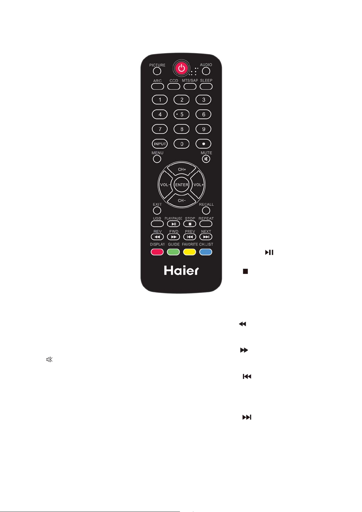
2.1 The Use of Remote Control
POWER
Press to power ON/OFF (standby) TV.
Note: The TV is never completely
powered off unless physically unplugged.
PICTURE
Press to change the picture mode: Vivid,
Standard, Eco, Movie, or Personal.
AUDIO
Press to change the audio mode:
Personal, Music, or Speech.
ARC
Press to change the aspect ratio: Normal,
Zoom1, Wide, Zoom2, or HDMI PC
mode(Only for HDMI Video Source).
CCD
Press repeatedly to change the closed
caption type: CC On/CC Off/CC On with
mute.
MTS/SAP
Press to activate the NTSC TV sounds.
(Switch Stereo, SAP or Mono tone for
ATV / switch audio languages for DTV.)
SLEEP
Press to set the preset time to switch the
TV to standby mode automatically (off / 5
10 / 15 / 30 / 60 / 90 / 120 / 180 /240
mins).
0 ~ 9 / • number
Press to enter TV channel number to
select channel (Press "•" to choose the
sub-channel).
INPUT
Press "INPUT" to open or toggle source
item in Input List.
MENU
Press to open or exit menu.
MUTE
Switch the sound on/off.
CH+ / CH -
• Menu is displayed: Press CH+ or CH- to
• Menu not displayed: Press CH+ or CH-
VOL+ / VOL-
• Menu is displayed: Press VOL+ or VOL-
• Menu not displayed: Press VOL+ or
navigate up or down.
to browse through the TV channels.
to navigate right or left.
VOL- to adjust volume.
EXIT
Press to exit menu or OSD.
RECALL
Press to display the previous channel.
DISPLAY
Press to show the information about the
input source, TV channel, display
resolution and current time.
GUIDE
Press to display the Electronic Program
Guide.
FAVORITE
Press "FAVORITE" to open or toggle
channel item in Favorite Channel List.
CH.LIST
Press to display the channel list.
For Multimedia use only.
USB
• For non JPEG/MP3 mode: Press to
display "Multimedia List" menu.
• For JPEG/MP3 mode: Press to toggle
MP3/JPEG mode.
PLAY/PAUSE
Press to Play/Pause in Multimedia source.
STOP
Press to Stop playing in Multimedia
source.
REPEAT
Press to toggle Repeat On/Off mode in
MP3 MusicBox.
REV
Press to go to the Previous folder / photo
in JPEG Viewer.
FWD
Press to go to the Next folder / photo in
JPEG Viewer.
PREV
Press to go to the First folder / photo in
JPEG Viewer. Press to skip current file
playing and play the previous file during
playing state in MP3 MusicBox.
NEXT
Press to go to the Final folder / photo in
JPEG Viewer. Press to skip current file
playing and play the next file during
playing state in MP3 MusicBox.
ENTER
Press to confirm a selection.
6
Page 7
2.2 To Use the Menus
1. Press the Menu button to display or close the main menu.
2. Use the Navigation Ring to move around to select, adjust or confirm an item in the OSD (On Screen Display)
menu.
Press the Menu button to enter the main OSD. Adjust the items including Video menu, Audio menu, Feature
menu, Channel menu, and VGA menu. However, some options in the menus may be unavailable in certain source
modes.
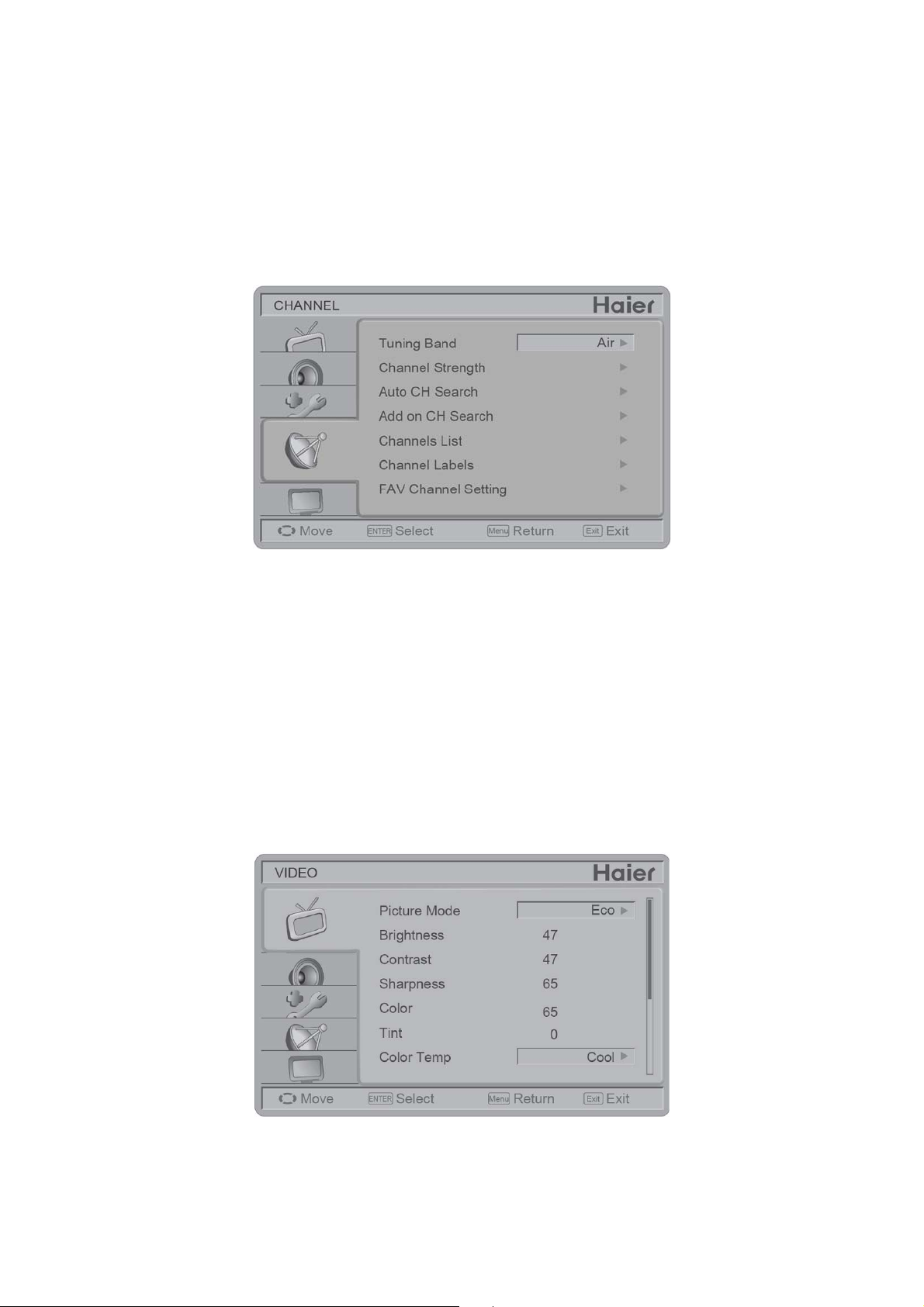
CHANNEL MENU
The Channel menu in TV mode is shown below.
1. Tuning Band: Select TV source signal from the Air (antenna) or Cable (CATV).
2. Channel Strength: Show the intensity of the received DTV signal.
3. Auto CH Search: Automatically scan all NTSC / ATSC TV channels and then store in the channel table. In
channel scan process, the OSD can display the number of channels which had been found.
4. Add on CH Search: Add channels which are newly found.
5. Channels List: Show the Channel List. You can select which channels are viewable.
6. Channel Labels: Shows the NTSC / ATSC TV Channel Labels. You can edit the labels.
7. FAV Channel Setting: Show the Favorite Channel List. You can add/remove channels from the favorites list.
VIDEO MENU
The Video menu in most source modes is shown below. It provides several video adjustment items for fine tuning
the video display. Only in VGA source mode, the Picture menu simply provides Picture Mode, Brightness,
Contrast, Color Temp, Noise Reduction, Backlight, Aspect Ratio, and Preset items.
1. Picture Mode: Select the picture mode: Vivid, Standard, Eco, Movie, or Personal (In VGA mode only support
Standard and Personal).
2. Brightness: Video brightness adjustment, the tuning range is 0 ~ 100.
3. Contrast: Video contrast adjustment, the tuning range is 0 ~ 100.
4. Sharpness: Video sharpness adjustment, the tuning range is 0 ~ 100.
7
Page 8
5. Color: Video color chroma adjustment, the tuning range is 0 ~ 100.
6. Tint: Video tint adjustment, the tuning range is R50 ~ G50.
7. Color Temp: Three color temperature modes. (Cool / Normal / Warm)
8. Noise Reduction: Select the noise reduction level: Low, Mid, High and Off.
9. Adaptive Contrast: Select On or Off to automatically adjust the contrast after analyzing the input signal.
10. DCR: Select On or Off to auto matically adjust the backlight of the screen.
11. Backlight: Backlight strength adjustment, the tuning range is 0 ~ 30.
12. Aspect Ratio: Select the aspect ratio: Normal / Zoom1 / Wide / Zoom2 / HDMI PC mode (Only for HDMI Video
Source).
13. Preset: Restore the default video settings.
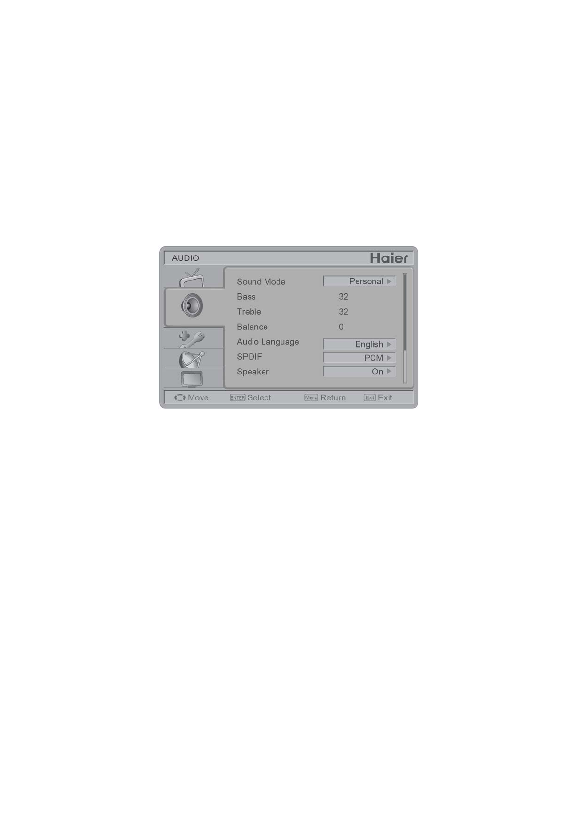
AUDIO MENU
The Audio menu in TV mode is shown below. It provides adjustments for modifying the audio setting. The audio
language setting is only available with ATSC (Digital) TV source, the option is disabled in other source modes.
1. Sound Mode: Select the audio mode: Personal, Music, or Speech.
2. Bass: Bass tone adjustment, the tuning range is 0 ~ 63.
3. Treble: Treble tone adjustment, the tuning range is 0 ~ 63.
4. Balance: Audio balance adjustment, the tuning range is L50 ~ R50.
5. Audio Source: Select the audio source: Stereo, SAP or Mono. (This function works in Analog TV only.)
6. Audio Language: Change the audio language setting for ATSC TV programs. The number of supported audio
languages depends on the ATSC TV program. (English / Spanish / French)
7. SPDIF: Digital audio output format. Select from RAW and PCM. (This function works in Digital TV only.)
8. Speaker: Choose to turn on / off the TV's intergrated speaker. The digital audio output signals and earphone
output signals will not be turned off even though the TV speaker is off. The default setting is On.
9. AVL: Choose On or Off to adjust volume to be consistent across programs and channels automatically.
10. Preset: Restore the default audio settings.
8
Page 9
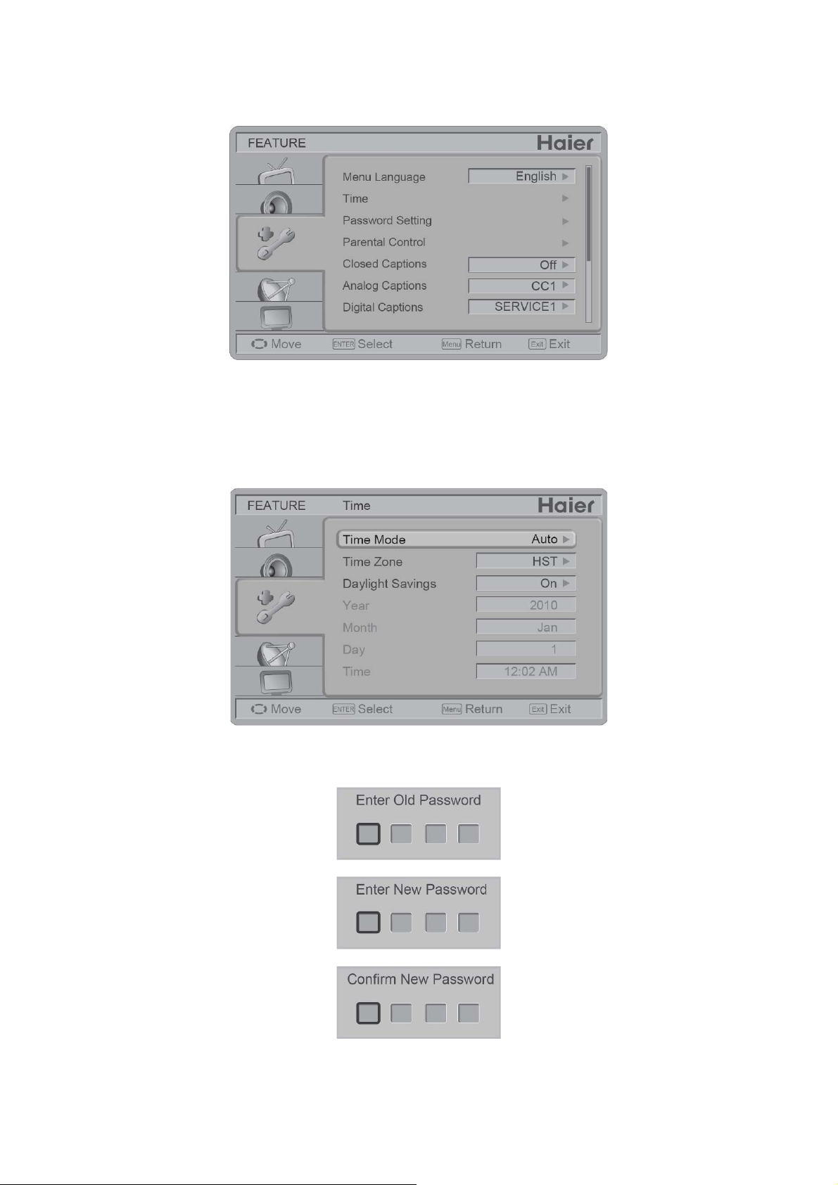
FEATURE MENU
The Feature menu is shown below. This menu contains options to set the language, time, and other settings.
Depending on the current mode (TV, HDMI, etc.), some options may not be available.
1. Menu Language: Select the menu display language. (English / Français / Español)
2. Time: Set current time. The sub-menu includes Time Mode, Time Zone, and Daylight Savings.
[Time Mode] – Select Auto or Manual. If Manual is selected you can set the Year, Month, Day and, Time
manually.
[Time Zone] – Set current time zone. (This item is available when Time Mode is set to Auto.)
[Daylight Savings] – Set to On or Off. (This item is available when Time Mode is set to Auto.)
3. Password Setting: Change the 4-numeral parental control password. Three steps are required for changing the
password: Enter Old Password –> Enter New Password –> Confirm New Password. Note: This option is only
available in TV, Composite and S-Video source modes. The default password is ό0 0 0 0ύ.
4. Parental Control: Provide the parental Control (V-chip) function setting. Before entering the Parental Control
sub-menu, enter the password first. Enter the Parental Lock item, then you can modify the MPAA or TV Rating table
to restrict viewing of certain programs. The blocked channels or source signals can be unlocked by entering the
password. Note: This feature is only available in TV, Composite and S-Video source modes. (The default password
9
Page 10
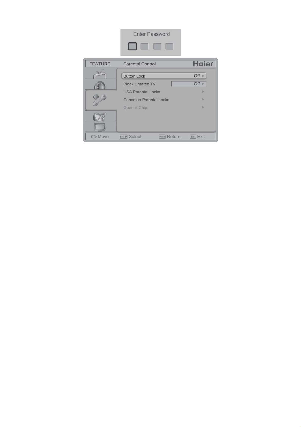
is 0 0 0 0.)
[Button Lock] – Select On or Off to lock or unlock the control buttons on the side panel of the TV. When this
function is enabled, the control buttons on your TV will be locked and the TV can only be controlled by the
remote control.
[Block Unrated TV] – When Block Unrated TV is set to on, your TV will block unrated programs.
[USA Parental Locks] – Set the parental control level by MPAA or TV Rating.
[Canadian Parental Locks] – Set the parental control level by English Rating or French Rating.
[Open V-Chip] – Open V-Chip is an advanced V-Chip rating system for digital channels that are received.
The rating table will be updated by program with RRT5 rating information.
5. Closed Captions: Select closed caption options. (Off / On / With Mute)
6. Analog Captions: Select analog caption options. (CC 1-4 / TEXT 1-4)
7. Digital Captions: Select digital caption options. (SERVICE 1-6) Note: This feature is only available in Digital TV
(ATSC) mode.
8. Digital Captions Setup: Provides numerous options for setting the digital closed caption style in the sub-menu.
Note: This feature is only available in Digital TV (ATSC) mode.
[Style] – Set to Automatic or Customer mode. If Customer mode is selected, you can modify the options
described below. The setting result will be shown immediately on the bottom of the sub-menu OSD.
[Size] – Digital closed caption font size, which can be set to Automatic, Small, Normal, or Large.
[Font] – Digital closed caption font style, which can be chosen as Automatic, Default, or Font 1 ~ 7.
[Text Color] – Automatic / White / Red / Green / Blue / Yellow / Magenta / Cyan / Black.
[Text Opacity] – Automatic / Solid / Flashing / Transparent / Translucent.
[Background Color] – Automatic / Black / White/ Red / Green / Blue / Yellow / Magenta / Cyan.
[Background Opacity] – Automatic / Solid / Flashing / Transparent / Translucent.
[Edge Effect] – Automatic / None / Raised / Depressed / Uniform / Left Shadow / Right Shadow.
[Edge Color] – Automatic / Red / Green / Blue / Yellow / Magenta / Cyan / Black / White.
9. Input Labels: This option is available only for non-TV sources. You can edit the input labels.
10. Component Setting: This option is only available in component input mode, which provides fine tuning of the
component display.
[Phase] – Adjust Picture Phase to reduce Horizontal-Line noise. The tuning range is from 0 to 31.
[Preset] – Restore the default component setting values.
11. MultiMedia Menu: This option shows the photos in JPEG formats and/or plays the music in MP3 formats that
are stored on a USB storage device. You can also use the USB time shift function.Note: File number is limited to
1000 files. Maximum JPEG sizes are:
For 19"/22": 10928 x 6114; For 24": 15360 x 8640
There are three ways to enter the JPEG Viewer and MP3 MusicBox interface:
10
Page 11
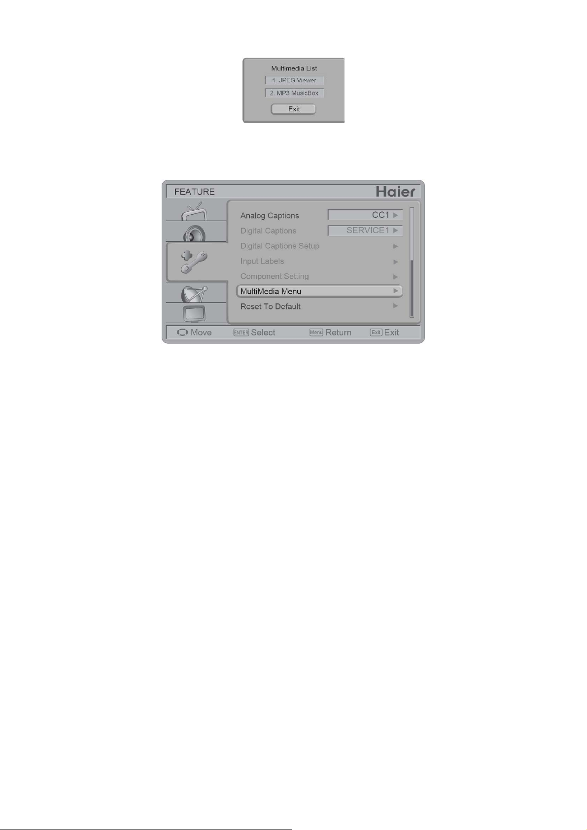
• After plugging a USB storage device into the USB port, the Multimedia List menu will be displayed.
• Select MultiMedia Menu in the Feature Menu to choose JPEG Viewer or MP3 MusicBox. These two items are
activated only if the USB storage device is plugged into the USB port.
• Once USB storage device is connected: Press the USB key to switch to the other multimedia mode. (JPEG
–>MP3 / MP3 –>JPEG)
[JPEG Viewer] – Press Menu to display the control menu. Press Enter to enlarge the selected photo (orange
frame) in browser.
• Image Delay: Set display time for each picture in the slide show mode. There are three options: Fast, Slow,
and Normal.
• Music On Slide Show: Enable background Music during the slide show. It will play the MP3 files in sequence
in the current folder repeatedly. The Music On Slide Show item will be grayed out if there are no MP3 files in
the current folder.
• Start Slide Show: Enter Slide Show mode.
• Rotate Photo: Rotate selected picture. (0/90/180/270)
• Back to Upper Folder: Return to the upper folder.
• Back to Root Folder: Return to root folder.
• Back to Browser: Return to Browser mode. (Photo page with control menu.)
• Exit: Exit JPEG Viewer and return to original source. (Browser with Control menu.)
[MP3 MusicBox]
• ListInfoBar (at the bottom): This part contains play list information: “Current Directory”, “Total File(s)”, “Total
Folder(s)”, “Current Item” in current directory and Key Help Bar.
• PlayList (on the right side): This part contains MP3 music files.
• ControlPanel (on the left side):
Bass, Treble, Balance, Volume: Adjust the audio tone.
Mute Screen: This provides an option for enabling (On) or disabling (Off) the auto
turn-off of the backlight while playing MP3 media. The setting is valid in the MP3 media player interface only.
After setting to On, the backlight will be turned-off automatically after 10 seconds if no key is pressed. Press
any key except POWER and the TV backlight will turn on again.
Preset: Resets all MP3 settings to the default values.
Exit: Exit MP3MusicBox interface.
[Time Shift] – The feature allows the viewer to pause and record the currently watched digital program (ATSC
or QAM) and resume to the point where it was paused. Insert the USB storage device to activate the Time Shift
function in the Feature menu.Note: – Formatting the USB 2.0 storage device will be needed. Save your original
data before formatting. All the data stored in the USB device will be erased after formatting.
– Sleep timer will be suspended if it had been set before Time Shift.
• USB Drive Storage
Format: Select to format the USB drive and locate an area for the Time Shift function.Note:
11
Page 12
• Format process will take at least 2 minutes. Please do not turn off the TV or remove the USB drive during
formatting.
• During formatting, a speed test will be done on the USB drive. If it fails, it means the USB disk may not
support the Time Shift function.
• Start Time Shift
Recording: Select to start the Time Shift function.Note:
• Please do not unplug the USB storage device when the Time Shift function is activated.
• Approximately 4GB of memory could buffer 180 minutes for 480i content or 30 minutes for 1080i content.
• Once 4GB of data gets stored, the time shift function will delete the stored data and restart the buffering of
content. This occurs even for USB devices larger than 4GB.
Note:
Time Shift limitations:
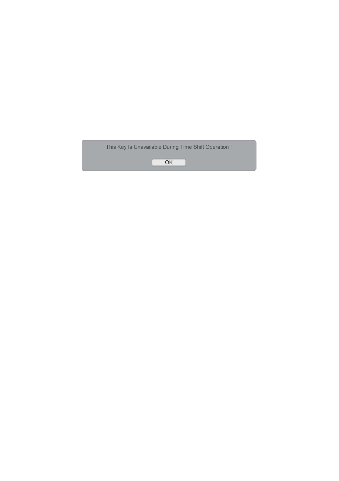
1. When the Time Shift feature is activated, only the PLAY/PAUSE/STOP/FWD/REV/VOL+/VOL-/MUTE
keys and some basic operation keys (ENTER/EXIT/navigation keys) are available. When a key is pressed
and that function is unavailable, the dialog box shown below will appear.
2. Video playback may not be smooth and skip if USB recording speed does not meet the minimum
requirements (for certain 1080i/p signals).
3. Do not remove USB disk or switch off the power during Time Shift operations. It will abort once the signal
is lost.
4. Do not remove the signal source during Time Shift operations.
5. Do not quickly and repeatedly change operations between PLAY/PAUSE/FWD/REV.
6. Sleep timer will be terminated if it had been set before Time Shift.
7. The USB storage size needs to be 4GB, 8GB or 16GB.
8. Video may become pixelated when Video bit rate is too low.
9. Close Caption setting is not available during Time Shift mode.
10. Not all USB devices are compatible. Below is a list of recommended USB drvies. Models that are not
listed may be compatible, but it is not guaranteed to work.
• SanDisk Extreme® Contour™ USB Flash Drive - 8GB SDCZ8-8192-E75
• SanDisk Extreme® Contour™ USB Flash Drive - 16GB SDCZ8-016G-A75
• Kingston DataTraveler 410 USB 2.0 Flash Drive - 8GB DT410/8GB
• Kingston DataTraveler 410 USB 2.0 Flash Drive - 16GB DT410/16GB
• OCZ Technology Rally2 USB 2.0 Flash Drive - 4GB OCZUSBR2DC-4GB
• OCZ Technology ATV USB 2.0 Flash Drive - 8GB OCZUSBATV - 8GB
• OCZ Technology Rally2 USB 2.0 Flash Drive - 8GB OCZUSBR2DC-8GB
11. This feature is not available for all digital TV, such as scrambled or audio only channels.
12. Reset to Default: Restore all settings to the factory default.
VGA MENU
This option is only shown and available while in VGA mode, which provides several options to fine tune the VGA
display.
1. H-Position: Adjust the horizontal position of the picture. (0-40)
2. V-Position: Adjust the vertical position of the picture. (0-16)
3. Clock: Adjust picture clock to reduce Vertical-Line noise. (0-16)
4. Phase: Adjust picture phase to reduce Horizontal-Line noise. (0-31)
5. Auto Adjust: Adjust the settings automatically.
6. Preset: Restore the default VGA setting values.
12
Page 13

2.3 Front Panel Control Knobs
1.
2.
3.
4.
5.
6.
7.
POWER
VOL +
VOL -
CH
CH
MENU
INPUT
Press to turn on / off (standby) the TV set.
Press to increase the volume.
Press to decrease the volume.
Press to increase the channel number.
Press to decrease the channel number.
Press to open or exit the OSD (on-screen display) menu.
Press to select the input source.
13
Page 14
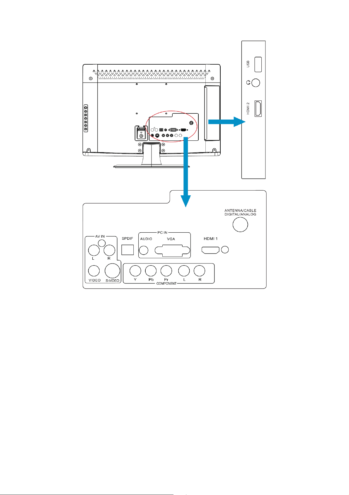
2.4 How to Connect
1. HDMI – Connect the primary source for digital video such as a DVD multimedia player or set top box through this
all digital connector.
2. PC IN – Connect the video and audio cables from a computer here.
3. AV IN (AV/S-VIDEO) – Connect the input source for composite video devices, such as a VCR or video game. Use
the white and red connectors to connect the external audio from the same source. The S-Video connection will take
priority over the Video RCA connector (yellow connector).
4. COMPONENT (Y/Pb/Pr with Audio L/R) – Connect the primary source for component video devices such as a
DVD Player or set top box here. Use red for Pr, blue for Pb, green for Y, red for right audio (R) and white for left
audio (L) inputs.
5. ANTENNA/CABLE DIGITAL/ANALOG – Connect to an antenna or digital cable (out-of-the-wall, not from Cable
Box) for Digital TV.
6. SPDIF (Optical Digital Audio Out) – When a digital audio signal is associated with the input selected for viewing,
the digital audio will be available on this SPDIF connection to your home theater system.
7. USB PORT – Insert USB storage device to the USB port to view JPEG photos, listen to MP3 music, or to run the
[Time Shift] function. (Please refer to page 22~24 for more information.)
8. Earphone Output – Connect to the headphones. When headphones are connected, the TV's intergrated
speakers will be muted.
Once your equipment is connected, use the following procedure to view the input signal: Press the INPUT button on
the remote control to select the relevant source to view.
(ex: Press INPUT button to select “Component” if you have connected a video recorder to the Component input.)
14
Page 15
V
T
T
T
T
T
T
T
T
T
T
T
T
3. Input/Output Specification
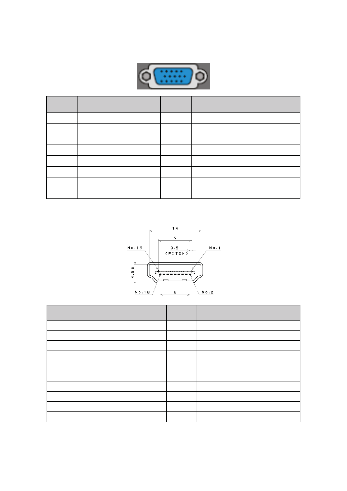
3.1 Input Signal Connector
D-SUB
HDMI
Pin No. Description Pin No. Description
1 Red Video 9 No Pin
2 Green Video 10 Sync Ground
3 Blue Video 11 SDA(Remote Control)
4 SCL(Remote Control) 12 Serial Data for DDC
5 Ground 13 H. Sync
6 Red Ground 14
7 Green Ground 15 Serial Clock for DDC
8 Blue Ground
. Sync
Pin No. Description Pin No. Description
1
2
3
4
5
6
7
8
9
10
MDS Data2+ 11
MDS Data2 shield 12
DMS Data2- 13 CEC
MDS Data1+ 14 NC
MDS Data1 shield 15 SCL
MDS Data1- 16 SDA
MDS Data0+ 17 DDC/CEC Ground
MDS Data0 shield 18 +5V Power
MDS Data0- 19 Hot Plug Detect
MDS Clock+
MDS Clock Shield
MDS Clock-
15
Page 16
3.2 Input Signal Timing
Analog RGB
LE19C1320
VESA MODES
Mode Resolution Total
640x480@60Hz 800 x 525 31.469 N 59.940 N 25.175
VGA
DOS 720x400@70Hz 900 x 449 31.469 N 70.087 P 28.322
SVGA
XGA
CVT-0.92M9 1280x720@60Hz 1664 x 748 44.722 N 59.855 P 74.500
WXGA 1280x768@60Hz 1440 x 790 47.396 P 59.995 N 68.250
WXGA 1360x768@60Hz 1720 x 795 75.000 P 60.020 P 162.000
640x480@72Hz 832 x 520 37.861 N 72.809 N 31.500
640x480@75Hz 840 x 500 37.500 N 75 N 31.500
800x600@56Hz 1024 x 625 35.156 P 56.250 P 36.000
800x600@60Hz 1056 x 628 37.879 P 60.317 P 40.000
800x600@72Hz 1040 x 666 48.077 P 72.188 P 50.000
800x600@75Hz 1056 x 625 46.875 P 75 P 49.500
1024x768@60Hz 1344 x 806 48.363 N 60.004 N 65.000
1024x768@70Hz 1328 x 806 56.476 N 70.069 N 75.000
1024x768@75Hz 1312 x 800 60.023 P 75.029 P 78.750
LE22/24C1380
Mode Resolution Total
640x480@60Hz 800 x 525 31.469 N 59.940 N 25.175
VGA
DOS 720x400@70Hz 900 x 449 31.469 N 70.087 P 28.322
SVGA
XGA
CVT-0.92M9 1280x720@60Hz 1664 x 748 44.722 N 59.855 P 74.500
WXGA 1280x768@60Hz 1440 x 790 47.396 P 59.995 N 68.250
SXGA 1280x1024@60Hz 1688 x 1066 63.981 P 60.020 P 108.000
WXGA+ 1440x900@60Hz 1600 x 926 55.469 P 59.901 N 88.750
WSXGA+ 1680x1050@60Hz 2240 x 1089 65.290 N 59.954 P 146.250
FHD 1920x1080@60Hz 2200 x 1125 67.500 P 60.000 P 148.500
640x480@72Hz 832 x 520 37.861 N 72.809 N 31.500
640x480@75Hz 840 x 500 37.500 N 75 N 31.500
800x600@56Hz 1024 x 625 35.156 P 56.250 P 36.000
800x600@60Hz 1056 x 628 37.879 P 60.317 P 40.000
800x600@72Hz 1040 x 666 48.077 P 72.188 P 50.000
800x600@75Hz 1056 x 625 46.875 P 75 P 49.500
1024x768@60Hz 1344 x 806 48.363 N 60.004 N 65.000
1024x768@70Hz 1328 x 806 56.476 N 70.069 N 75.000
1024x768@75Hz 1312 x 800 60.023 P 75.029 P 78.750
Horizontal Vertical
Nominal
Frequency
(KHz)
VESA MODES
Horizontal Vertical
Nominal
Frequency
(KHz)
Sync
Polarity
Sync
Polarity
Nominal
Freq.
(Hz)
Nominal
Freq.
(Hz)
Sync
Polarity
Sync
Polarity
Nominal
Pixel
Clock
(MHz)
Nominal
Pixel
Clock
(MHz)
16
Page 17
HDMI
LE19C1320
VESA MODES
Mode Resolution Total
DOS 720 x 400@70Hz 900 x 449 31.469 N 70.087 P 28.322
VGA 640 x 480@60Hz 800 x 525 31.469 N 59.940 N 25.175
SVGA 800 x 600@60Hz 1056 x 628 37.879 P 60.317 P 40
XGA 1024 x 768@60Hz 1344 x 806 48.363 N 60.004 N 65
WXGA 1280 x 768@60Hz 1664 x 798 47.396 P 59.995 N 68.25
CVT-0.92M9 1280 x 720@60Hz 1664 x 748 44.772 N 59.855 P 74.5
WXGA 1360x768@60Hz 1720 x 795 75.000 P 60.020 P 162.000
1080P 1920 x 1080P 2200 x 1125 67.5 60, 148.5
720P 1280 x 720P 1650 x 750 45.00 60, 74.25
1080i 1920 x 1080i 2200 x 1125 33.75 60, 74.25
480P 720 x 480P 858 x 525 31.50 60, 27.03
480i 720 x 480i 1716 x 525 15.75 60, 13.51
LE22C1380
Mode Resolution Total
DOS 720 x 400@70Hz 900 x 449 31.469 N 70.087 P 28.322
VGA 640 x 480@60Hz 800 x 525 31.469 N 59.940 N 25.175
SVGA 800 x 600@60Hz 1056 x 628 37.879 P 60.317 P 40
XGA 1024 x 768@60Hz 1344 x 806 48.363 N 60.004 N 65
WXGA 1280 x 768@60Hz 1664 x 798 47.396 P 59.995 N 68.25
CVT-0.92M9 1280 x 720@60Hz 1664 x 748 44.772 N 59.855 P 74.5
SXGA 1280 x 1024@60Hz 1688 x 1066 63.981 P 60.02 P 108
WXGA+ 1440 x 900@60Hz 1904 x 934 55.469 P 59.901 N 88.75
WSXGA+ 1680 x 1050@60Hz 1840 x 1080 65.29 N 59.954 P 146.25
FHD 1920x1080@60Hz 2200 x 1125 67.500 P 60.000 P 148.500
1080P 1920 x 1080P 2200 x 1125 67.5 60, 148.5
720P 1280 x 720P 1650 x 750 45.00 60, 74.25
1080i 1920 x 1080i 2200 x 1125 33.75 60, 74.25
480P 720 x 480P 858 x 525 31.50 60, 27.03
480i 720 x 480i 1716 x 525 15.75 60, 13.51
Horizontal Vertical
Nominal
Frequency
(KHz)
VESA MODES
Horizontal Vertical
Nominal
Frequency
(KHz)
Sync
Polarity
Sync
Polarity
Nominal
Freq.
(Hz)
Nominal
Freq.
(Hz)
Sync
Polarity
Sync
Polarity
Nominal
Pixel
Clock
(MHz)
Nominal
Pixel
Clock
(MHz)
17
Page 18
LE24C1380
VESA MODES
Mode Resolution Total
DOS 720 x 400@70Hz 900 x 449 31.469 N 70.087 P 28.322
VGA 640 x 480@60Hz 800 x 525 31.469 N 59.940 N 25.175
SVGA 800 x 600@60Hz 1056 x 628 37.879 P 60.317 P 40
XGA 1024 x 768@60Hz 1344 x 806 48.363 N 60.004 N 65
WXGA 1280 x 768@60Hz 1664 x 798 47.396 P 59.995 N 68.25
CVT-0.92M9 1280 x 720@60Hz 1664 x 748 44.772 N 59.855 P 74.5
SXGA 1280 x 1024@60Hz 1688 x 1066 63.981 P 60.02 P 108
WXGA+ 1440 x 900@60Hz 1904 x 934 55.469 P 59.901 N 88.75
WSXGA+ 1680 x 1050@60Hz 1840 x 1080 65.29 N 59.954 P 146.25
1080P 1920 x 1080P 2200 x 1125 67.5 60, 148.5
720P 1280 x 720P 1650 x 750 45.00 60, 74.25
1080i 1920 x 1080i 2200 x 1125 33.75 60, 74.25
480P 720 x 480P 858 x 525 31.50 60, 27.03
480i 720 x 480i 1716 x 525 15.75 60, 13.51
Horizontal Vertical
Nominal
Frequency
(KHz)
Sync
Polarity
Nominal
Freq.
(Hz)
Sync
Polarity
Nominal
Pixel
Clock
(MHz)
18
Page 19

4. Mechanical Instructions
LE19C1320
TBD
19
Page 20
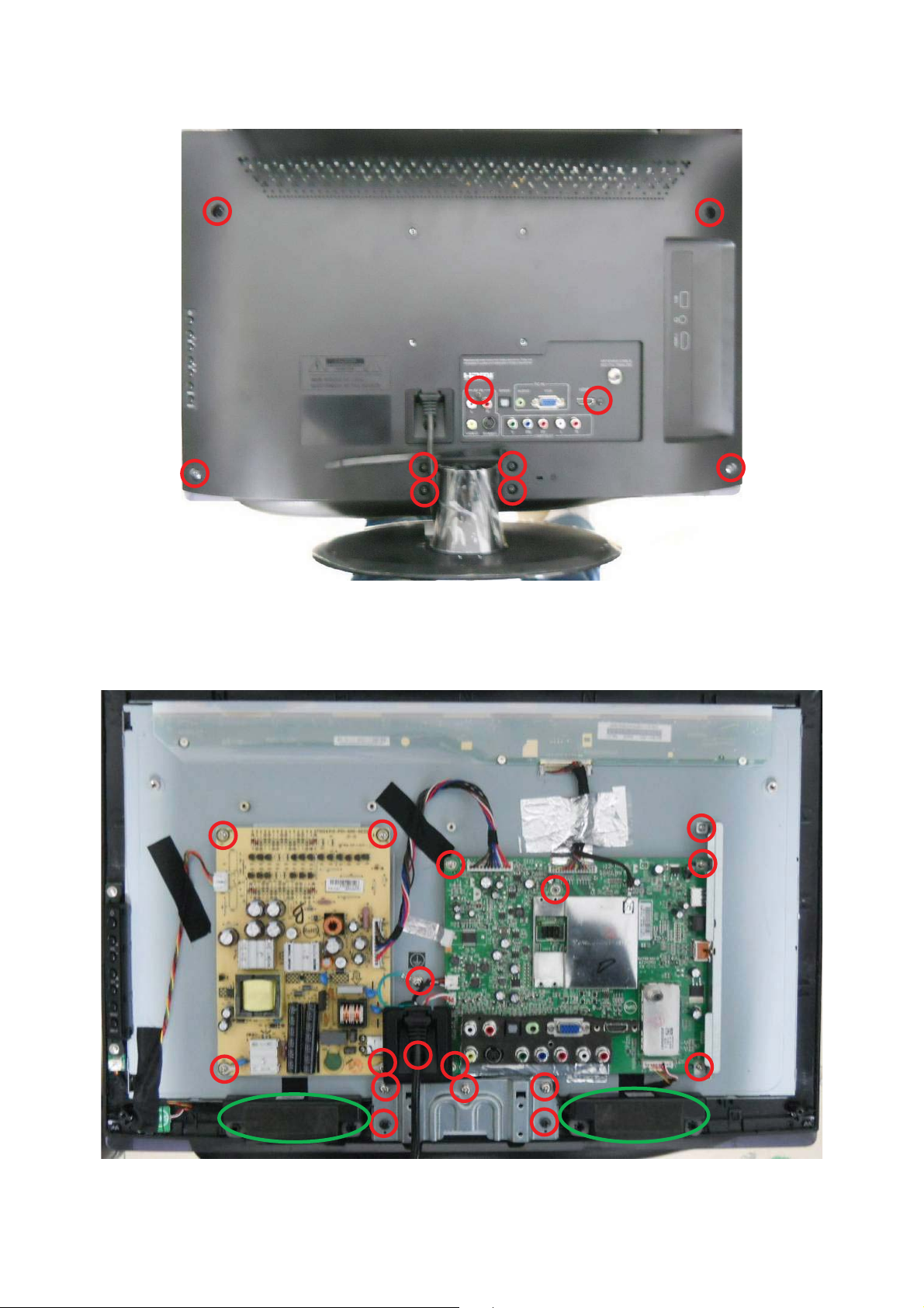
LE22C1380
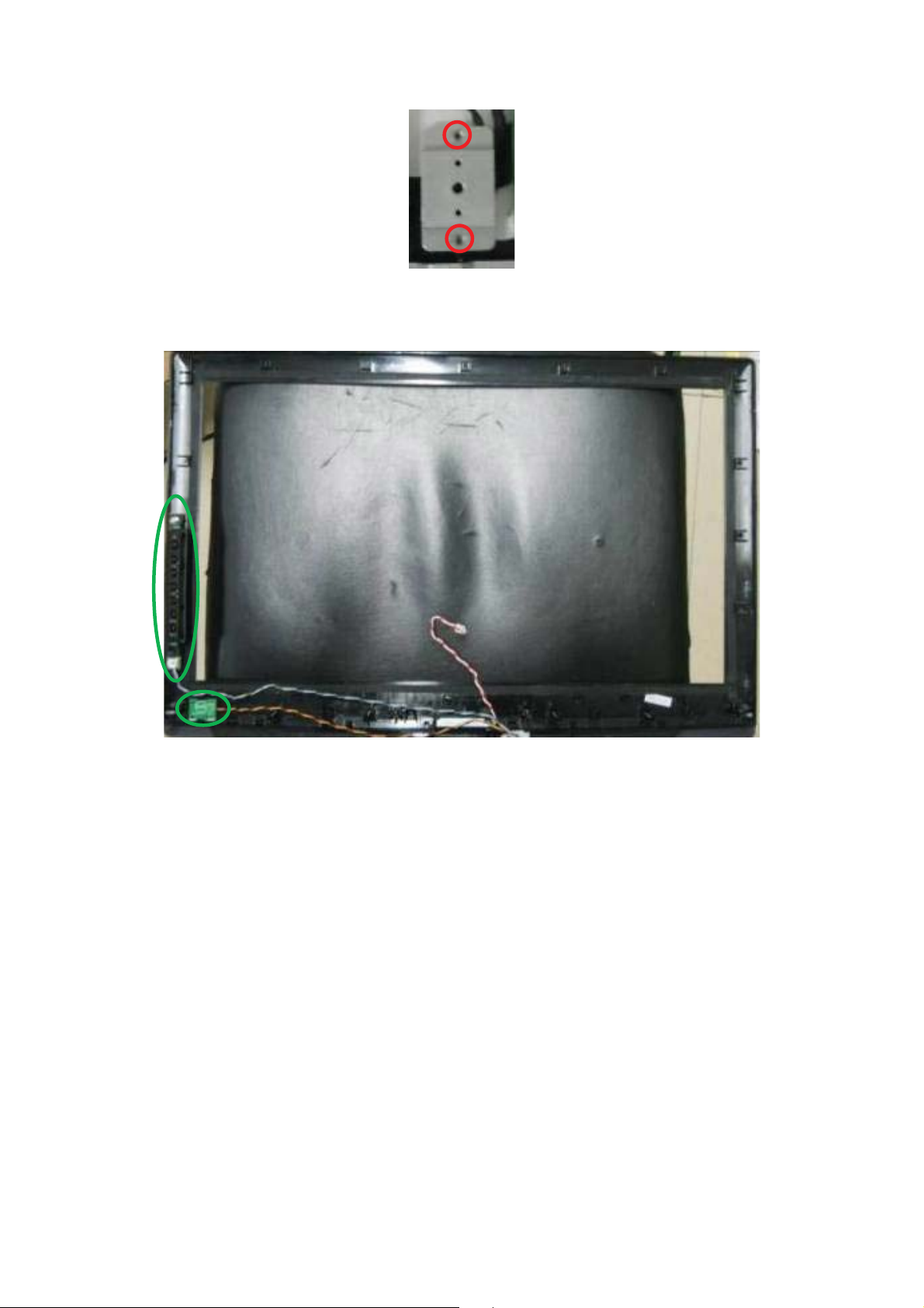
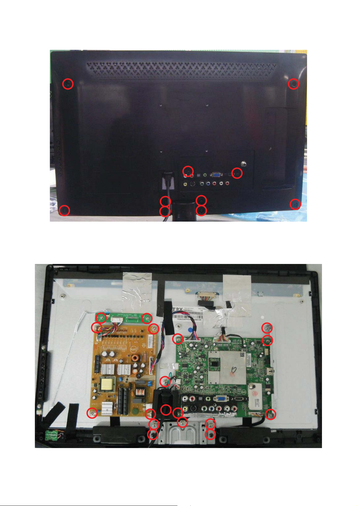
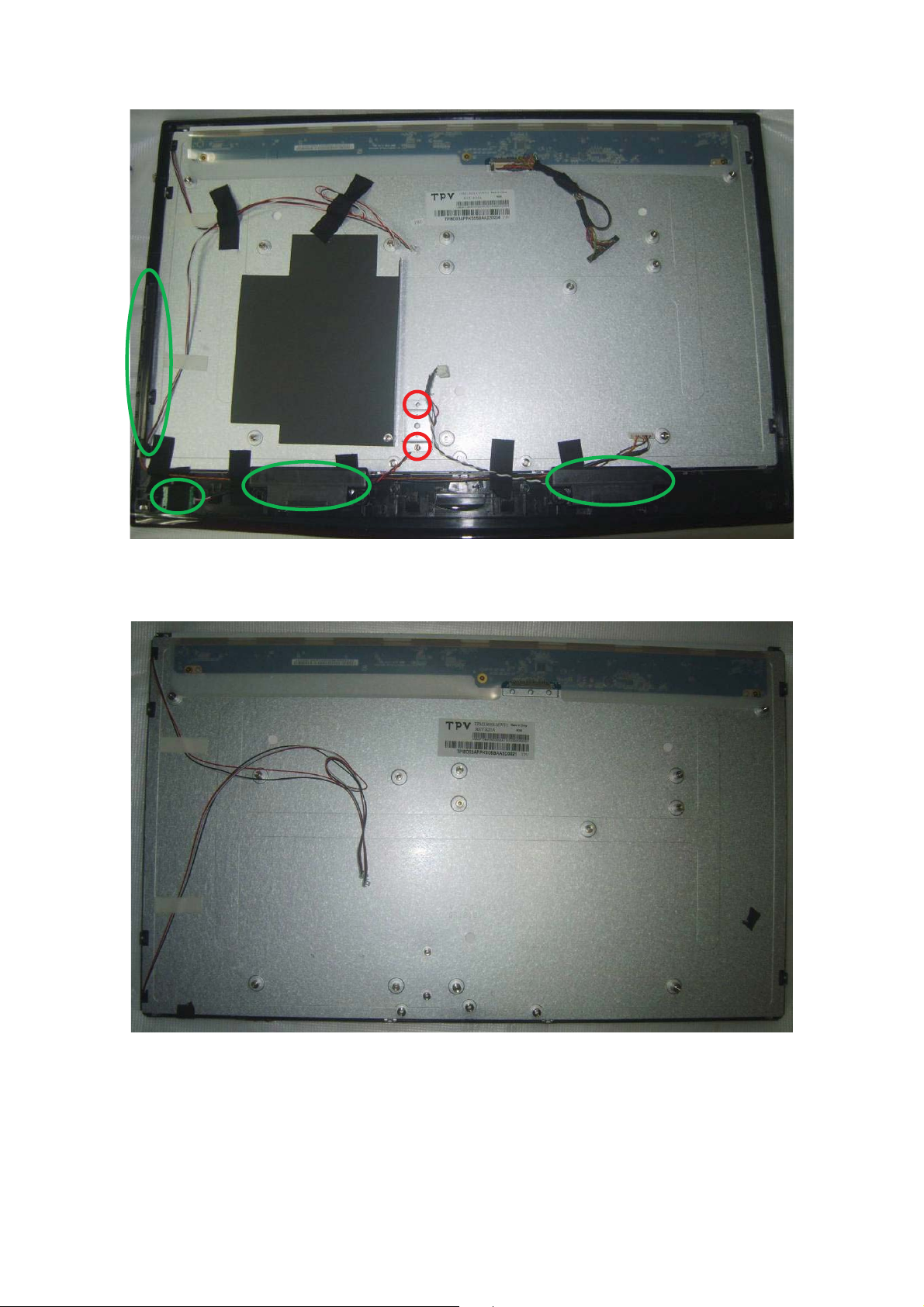
Step1. Remove the STAND ASS’Y and REAR COVER.
Step2. Remove the AC COVER, HINGE BKT, INVERTER BOARD, MAIN BOARD, POWER BOARD
and SPEAKERS and separate BEZEL and PANEL.
20
Page 21
Step3. Remove the AC BKT.
Step4. Remove KEY BOARD and IR BOARD.
21
Page 22
LE24C1380
Step1. Remove the STAND ASS’Y and REAR COVER.
Step2. Remove the AC COVER, HINGE BKT, INVERTER BOARD, MAIN BOARD and POWER
BOARD.
22
Page 23
Step3. Remove the AC BKT, KEY BOARD, IR BOARD and SPEAKERS.
Step4. The PANEL.
23
Page 24

p
p
5. Repair Flow Chart
1. No power
No power (LED “Off”)
Check the AC input and
the
ower is “ON”?
Yes
Power board
out
ut=5.2V?
Yes
Check the IR board and LED
Replace the IR board
No
Replace the main board
No
Power “On”
No
Replace the power board
24
Page 25

2. Can’t start
Can’t start˄LED red˅
Power board output᧹12/16V?
Yes
Check the power key is under control?
No
Check the IR receiver is normal?
No
Replace the power board
Yes
Replace the key board
Yes
Replace the IR board
No
Replace the main board
No
Replace the Power board
25
Page 26

3. Abnormal Display
Abnormal Display
Check the source
Yes
Enter factory mode to do
“EEPROM initial”&“Reset”
No
No
Reset the source
Check the main board
Yes
Check the LVDS cable
Yes
Check the panel
No
Replace the panel
No
Replace the main board
No
Replace the LVDS cable
26
Page 27

4. No display
No display (LED white)
Check TV is under control and power
on/off by remote control and power key?
Yes
Check the LVDS cable
Yes
Yes
Check the backlight is
“On”?
No
Reinsert or replace the
LVDS cable
No
No
Check the B/L
signal is available?
Yes
Replace the main board
No
Replace main board
Panel Vcc = 5V?
Yes
Replace the Panel
No
Replace the main board
Power board output᧹12/16V?
Yes
Replace the Panel
Replace the power board
No
27
Page 28

5. Sound problem
No sound or sound abnormal
Check the audio source connection
and the TV system are correct?
Yes
Check the TV is muted, adjust the
volume or enter the menu to reset?
No
No
Reinsert the audio cable or
change the TV system
Enter factory mode to do “Reset”
No
Check the cable between the
speakers and main board is OK?
Yes
Check the speaker resistance value is in spec
(Remark: The value is marked on the speaker)?
Yes
Replace the cable
Replace the main board
No
No
Replace the speaker
28
Page 29

6. Remote control malfunction
Remote Control malfunction
Check the remote control battery is
not properly placed or no power?
No
Use the other remote controls
No
Whether the IR board is
abnormal?
No
Replace the main board
Yes
Replace the battery
Yes
Replace the remote control
Yes
Replace the IR board
29
Page 30

7. OSD is unstable or can’t work normally
OSD is unstable or can’t work normally
Key board connected properly?
Yes
Buttons are OK?
Yes
Key board is OK?
Yes
Enter factory mode to do “Reset”
No
No
No
No
Reconnect the key board
Replace the button function
Replace the key board
Replace the main board
30
Page 31

6. PCB Layout
6.1 Main Board
715G3759M02000005K
31
Page 32

32
Page 33

6.2 Power Board
LE19C1320 715G3762P01W32002S
33
Page 34

34 35
Page 35

Page 36

LE22C1380 715G4313P01000003S
36
Page 37

37
Page 38

38
Page 39

LE24C1380 715G4147P01H21002S
39
Page 40

40 41
Page 41

Page 42

6.3 Key Board
715G4105K01000004L
6.4 IR Board
715G4104R01000004S
42
Page 43

7. Adjustment
7.1 ADC Adjustment
It’s no need to adjust the white balance for this model, do ADC only.
Step1: Turn on the TV, press “Menu”, then press number key 1 Æ 9 Æ 9 Æ 9 and “ENTER”, it will achieve the factory
mode. Take the following picture for example:
Step2: Change TV, press the “Current Source” to Component mode and change signal to 1080i mode, press the
“Auto Color”;
Step3: Change TV, press the “Current Source” to PC mode and change signal to PC TIMING 137(1024X768);
Pattern 147 (16 Grays), press the “Auto Color”.
43
Page 44

7.2 FW Upgrade
Step 1: Ready for F/W Upgrade
1.1 Prepare a USB memory (The file system of USB memory must be FAT16 or FAT 32).
1.2 Copy the FW from your computer to the USB memory, and remove it from computer’s USB port!
1.3 Note: 1). Note the version of this F/W is V2.01 before upgrade.
2). The software file name must content three parts, the first is brand, the second is customer model
name and the third is FW version. The first and second parts of FW name must be the same as the
TV, and the third part must not be the same as TV current FW version. Or the FW upgrade can’t
continue. Take Haier L19C1120 for example:
Step 2: F/W Upgrad
2.1 AC on (Power plug Figure 2.1/2.2)
Brand: Haier Customer model name
FW version: V2.01
Figure 2.1 Figure 2.2
2.2 Plug the USB memory on the USB port on the side I/O port of TV. (Figure 2.3)
Figure 2.3
44
Page 45

2.3 Press the power key on the Remote Control or the right side of TV to turn on TV.
Figure 2.4 fig2.5
2.4 When TV detects the USB memory, there is a prompt frame appearing on the screen as figure 2.6, press
“ENTER” key(on the Navigation Keys on the Remote control, as follows Figure 2.7 to select “Yes” option to
download F/W(Figure 2.8). Take Haier L19C1120 for example:
Figure 2.6
Figure 2.7
45
Page 46

2.5 TV will upgrade automatically.
Note: When Upgrade on the process, please don’t Power-Off! (Figure 2.8)
Figure 2.8
2.6 When upgrade 100% and prompt for Upgrade Success info, remove the USB Drive and press “ENTER” key
to reset TV (Figure 2.9)
Figure 2.9
Step 3: Check the F/W version and reset to default.
3.1 Press “MENU”+”1”+”9” +”9” +”9” +”ENTER” key rapidly on the Remote control to enter the factory mode
(Figure 3.1)
Do the following steps rapidly:
1. Press “MENU”;
2. Press”1”+”9” +”9” +”9”;
“
Figure 3.1
46
”
Page 47

3.2 Check the F/W version on the second row of the factory mode info. If F/W version is incorrect, please
upgrade again as above steps, else let’s go to Step 3.3. Take Haier HLC24XLE2 for example:
Figure 3.2
3.3 If the FW version is correct, please do factory reset.
Choose “Reset” and press “ENTER” key to do factory reset as figure 3.3 to figure 3.5.
Press “ENTER”,
Show “Doing”
Figure 3.3 figure 3.4
Figure 3.5
3.4 After all the steps, FW upgrade is finished finally.
Show “Done”
Reset ok!
47
Page 48

7.3 The Writing VGA & HDMI EDID
Step1. Ready for writing EDID
Tool: 715G2005-C2
Cable: a LPT cable, a VGA cable, a DVI to HDMI cable and a 12V DC adapter.
715G2005-C2 male to male LPT cable
VGA cable DVI to HDMI cable
Step2. Connection for writing VGA EDID.
Connect to PC LPT port.
Connect to TV VGA port.
48
12V DC input
Page 49

Step3. Install TPV edid tool. Take Haier LY19Z6 for example:
1. Click here to open this interface.
This red frame contents detail information in VGA EDID file.
1. Double click this icon to install. 2. Double click this icon to run.
3. Click anyone file to
add VGA EDID file.
4. Click here to Read the file
2. Choose the VGA EDID file.
49
Page 50

Step4. Click “FPD” to open another interface as follows. Take Haier LY19Z6 for example:
1. Tick LPT1
2. Click here to read file as figure 4.2
2. Click “open” to read the “.dat” file.
figure 4.2
50
Page 51

Step5. Click “write EDID” to write EDID. If display “NG” in the yellow blank, which represent writing failly. Please
check the whether the connection of tool and cables is nomal and retry. Another way is to change a new ISP board
and retry. Take Haier LY19Z6 for example:
2. “OK” represents writing successfully.
3. Click “Read EDID” can read
out the EDID info checked in
“Edid Conten” interface.
1. Click here to write EDID.
Write fail.
51
Page 52

Step6. Write HDMI EDID.
Connection for writing HDMI EDID.
Connect to PC LPT port.
Connect to TV HDMI port.
Notice: When writing HDMI EDID, the TV must be AC on, or the process can’t continue, and will prompt
“NG” info.
The other steps refer to the writing VGA EDID sop.
12V DC input
52
Page 53

Main Board Power System
Max. 2A
For ZR39787HGCF uMCU
TU101 ENV56U03D8F Fo r TUNER+5V
5VT
For Audio Amplifier
9V
P24V/16V
TDA7491P13TR
PANEL Inve rte r
P24V/16V
For TUNER+5V
U708 G9084-50TU3U
TU101 ENV56U03D8F
PANEL LVDS Powe r
5VT
Q403 AO 4449
U706 G5655P12U
U708 G9084-50TU3U
P12V
U401 ZR39787HGCF
1V8_STB
For ZR39787HGCF uMCU
PANEL LVDS Powe rQ403 AO 4449
+5VSB
U401 ZR39787HGCF
U702 AZ1084D-1.8TRE1
For VGA EDID
3V3_STB
U701 G5622ADJT11U
U105 M24C02-WDW6P
For USB OCP
USB5V
U409 G5250K1T1U
VCC5D
Q703 AO4449
For EEPROM
For SPI Flas h
For ZR39787HGCF
For Audio Headphone Am plifier
U406 CAT24C64WI-GT3
U401 ZR39787HGCF
D3V 3
5V_HP
U703 G1084-33T43Uf
U606 MAX9728AETC+
U405 MX25L3205DM2I-12G
For DDR II
For ZR39787HGCF
U401 ZR39787HGCF
U402, U403
H5PS5162FFR-S6C
U401 ZR39787HGCF For ZR39787HGCF
D1V 8
VCC1V1
U704 G5692P11U
U705 G5692P11U
19", 22", 24"
1V8_STB
Max. 1A
Max. 3A
U702
AZ1084D-1.8TRE1
3V3_STB
D3V3
U703 G1084-33T43Uf
U701 G5622ADJT11U
VCC5D
+5VSB
AO4449
Max. 2.5A
STB 15m A
Function9BL_BRI_ADJ
BL_ON_OFF
NC
NC
4
3
1
Pin
2
Power Board Input : +5VSB, P16V
Max. 2A
Max. 2A
D1V8
VCC1V1
U705 G5692P11U
U704 G5692P11U
P16V
Max. 1.5A
POWER
BOARD
GND
GND
5
16V
16V
GND
8
7
6
5.2V
NC
5.2V
11
12
10
Max. 2A
5VT
U708 G9084-50TU3U
9V
U706 G5655P12U
Audio Amplifier
D16V
AO4449
Max. 2A
Max. 2A
53
1V8_STB
LVDS
SPEAKER
Audio Amplifier
LCD PANEL
DDRII * 2
H5PS5162FFR-S6C
GPIO
FLASH ROM
MX25L3205DM2I-12G
CAT24C64WI-GT3
EJTAG
ZR39787HGCF
EarPhone Output
S/PDIF Output
Max. 1A
U702
TDA7491P13TR
Earphone Amplifier
MAX9728AETC+
3V3_STB
U701 G5622ADJT11U
+5VSB
Max. 2.5A
STB 15mA
Max. 2A
AZ1084D-1.8TRE1
Max. 3A
D3V3
U703 G1084-33T43Uf
VCC5D
AO4449
D1V8
Max. 2A
VCC1V1
U705 G5692P11U
U704 G5692P11U
System Block Diagram
Hsync, Vsync
RGB
YPbPr
CVBS
Y/C
DVD Y/C
S-VIDEO
VIDEO
VIF
Tuner
ENV56U03D8F
Y/C
SN74LVC1G17
I2C
VGA
YPbPr
TMDS
TMDS
Function
BL_BRI_ADJ
BL_ON_OFF
Pin
M24C02
HDMI-1
AV AUDIO-R\L
HDMI-2
DVD AUDIO-R\L
VGA AUDIO-R\L
YPbPr AUDIO-R\L
1
Power Board Input : +5VSB, P19V
Comb TV
POWER
BOARD
DVD_5V
19V
GND
GNDNCDVD_5V
GND
8765432
9
5VT
U708 G9084-50TU3U
DVD Comb
12V
Audio Amplifier
U706 G5655P12U
19V
19V
19V
Max. 1.5A
+5V_SSB
PS_ON
19V
12
11
10
13 +5V_SSB
8. Block Diagram
26"
Power Board
Input :
+5VSB, P12V,
Function
Pin
P24V
BL_ON_OFF
6
4
1
3
7
24V5PWR_ON_STB
9108
5.2V
5.2V
12
11
GND
24V2GND
GND
12V
BL_BRI_ADJ
12V
Page 54

Panel
10 Pin
CN401
095G801832D904
LVDS Cable
32 Pin
CN408
12 Pin
CN701
U401
Scaler IC
ZR39787HGCF
54
CN606
095G801313D683
HARNESS
To Panel
4 Pin
13 Pin
CN902
CN903
Speaker R/L
3Pin
CN201
Power Board
10 Pin
CN904
Key
Board
4 Pin
CN001
IR Board
9. Wiring Diagram
LE19C1320
Page 55

Panel
095G801832X902
LVDS Cable
32 Pin
CN408
CN701
12 Pin
U401
ZR39787HGCF
Scaler IC
10 Pin
CN401
55
CN606
095G801313D683
HARNESS
To Panel
4 Pin
13 Pin
CN902
CN901
Speaker R/L
3Pin
CN201
Power Board
6 Pin
CN906
Key
Board
4 Pin
CN001
IR Board
LE22C1380
Page 56

Panel
0
095G801832X903
LVDS Cable
32 Pin
CN408
12 Pin
CN701
U401
ZR39787HGCF
Scaler IC
10 Pin
CN401
56
CN606
095G801313L678
HARNESS
Inverter Board
CN801
10 Pin
CN802
To Panel
6+6 Pin
CN903
4 Pin
13 Pin
CN901
CN904
Speaker R/L
3Pin
CN201
Power Board
IR Board
Key
Board
4 Pin
CN001
LE24C1380
Page 57

U401P
VGA_R 4
VGA_G 4
Demodul ator
IF_AINN
IF_AINP
SIF_AI NN
SIF_AI NP
AF4
AE4
SIF_N
SIF_P
0402
0402
C102 10N 50V
C105 10N 50V
IF_RBIAS
IF_VINBIAS
IF_VCM
AF2
AE2
AD3
AD2
AD1
IF_AINN
IF_AINP
0402
0402
C111 100N 16V
C112 100N 16V
R106 3.9K 1/10W
0402
C107 1N 50V
0402
C110
82pF 50V
L102
0.15uH 5%
0402
R103 47 OHM 1/16W
0402
0402
L101
0.082uH
C115 100pF 50V
C109 100pF 50V
MPEG _FA IL
DEMOD_CLKO
IF_VREFN
IF_VREFP
AF1
AE1
AC8
AC7
AD8
1
1
0402
0402
TP2
TP1
C113 100N 16V
C114 100N 16V
R108 33 OHM 1/10W
D3V3
0402
C108 1N 50V
1 2
0402
R107 47 OHM 1/16W
L103
0.082uH
IF_AGC
RF_AGC
DMOD_RST_N
PARAM0
SA_DATA
AC6
DEMOD_RSTN7
IF_DVAL_GPIO
ZR39787HGCF
AF7
AF8
AE7
AA5
PARAM0
Place R111 & C119
close to U401
R111 2K 1/10W
R109 4.7K 1/10W
C119
100N16V
0402
IF_AGC
3
2
I/O2
I/O34VDD5I/O4
U10 8
AZC19 9- 04S
VCC5D
CN10 1
I2C1_SCL 6,9
I2C1_SDA 6,9
I2C1_SDA
I2C1_SCL
R102
D3V3
NC/10K 1/10W
R101
NC/10K 1/10W
R113 220 OHM 1/10W
R112 220 OHM 1/10W
UART0_RX
UART0_TX
UART0_RX6
UART0_TX6
VGA_B 4
VGA_G
VGA_B
VGA_R
1
I/O1
GND
6
1 2FB102 60 OHM
1 2FB103 60 OHM
1 2FB104 60 OHM
0402
C153
18pF 50V
C152
18pF 50V
0402
C151
18pF 50V
R119
R118
R117
VGA5V
162738495
1716
1112131415
ZD101
1 2
C120
10
VPORT0603100KV05
U10 9
VGA_HSYNC_DET 7
VGA_HSYNC_DET
SN74LVC1G17DBVR
U10 4
53
2 4
3V3_STB
0402
C124
100N16V
RGB_HSYNC
0402
75R 1/10W 1%
75R 1/10W 1%
75R 1/10W 1%
100N16V
0402
VGA_HSYNC
DB15
88G 35315F CL
53
D3V3
1
3
2
I/O1
I/O2
GND
I/O34VDD5I/O4
AZC1 99 -04 S
6
VCC5DC122
R122
2.2K 1/10W
R121
2.2K 1/10W
C123
100N16V
0402
RGB_HSYNC
3V3_STB
VGA_HSY NC 4
NC/22pF
C126
R123 33 OHM 1/10W
SN74LVC1G17DBVR
U10 3
D3V3
2 4
VGA_VSYNC_D ET 7
VGA_VSYN C_DETRGB_VSYNC
SN74LVC1G17DBVR
U10 7
53
2 4
C128
100N16V
0402
RGB_VSYNC
VGA_VSYN C 4
VGA_VSYNC
C129
NC/22pF
R129 33 OHM 1/10W
SN74LVC1G17DBVR
U10 6
53
2 4
0402
C127
100N16V
VGA_EDID _WP 7
57
R105 100 OHM 1/10W
C104
5VT
C103
C101
1
NC
TUNER
TU101
13211
14
ENV56U03D8F
ET-29DHRV
10. Schematic Diagram
10.1 Main Board
715G3759M02000005K
03) Tuner/VGA Inputs
R104 100 OHM 1/10W
1UF16V
2N2 50V
0402
100N16V
C106 2N 2 50V
9
3
2
+B
12
10
6
5
11
NC
SCL
SDA
BT Monitor
RF-AGC Monitor
10
6
9
5
IF_AGC
IF_AP
IF_AN
0402
C118
100N16V
C117
22P 50V
C116
22P 50V
14
12
IF AGC
IFD-out113IFD-out2
TH1
IF Monitor
TH2
TH3
TH4
1
3
5V: +B = 150mA(MAX)
TU_ GND
15
16
TU_G ND
17
18
I2C Bus Address
#C2H (Write Mode)
#C3H (Read Mode)
R115 1K 1/10W
R114 100 OHM 1/10W
R120 100 OHM 1/10W
R116 1K 1/10W
NC/47pF
C121
NC/ 330pF
VGA_SCL
VGA_SDA
RGB_VSY NC
RGB_HSYNC
ZD102
BAT54C
2
+5VSB
VGA5V
3
1
C125
VGA_5V
VGA_EDID _WP
R127 33 OHM 1/10W
R126
1K 1/10W
R128
10K 1/10W
R125
4.7K 1/10W
R124
4.7K 1/10W
VGA_SCL
VGA_SDA
5
6
7
8
WP
SCL
SDA
VCC
0.22uF 25V
A01A12A23GND
U10 5
AT24 C02 BN-SH-T
4
VGA Input
Page 58

A
Vide o In I/F
SVIDEO0YU3SVIDEO0C
SVIDEO1YU4SVIDEO1C
U401F
V3
V4
0402
0402
0402
0402
C169 NC/220N 10V
C170 NC/220N 10V
C165 220N 10V
C166 220N 10V
CVBS0
CVBS1
SVIDEO2YU5SVIDEO2CV5CVBS2
AA3
AB3
AB4
0402
C132 220N 10V
C133
CVBS3
AA4
0402
NC/22pF
Place parts very close to U401
DVD_S_C
AV_CVBS
1 2FB112 NC/ 30 OHM
R180
NC/75R 1/10W 1%
R179
NC/75R 1/10W 1%
AV_S_Y
AV_S_C
1 2FB111 NC/ 30 OHM
DVD_S_Y
SOY_IN0
VIN_R1U2VIN_G1U1VIN_B1V1SOY_IN1
V2
0402
0402
0402
0402
C137 10N 50V
C136 220N 10V
C134 220N 10V
C135 220N 10V
C140
NC/22pF
C139
NC/22pF
C138
NC/22pF
YPbPr_Pb
YPbPr_Pr
YPbPr_Y
VIN_R2W2VIN_G2W1VIN_B2Y1SOG_IN0
VGA_R0T2VGA_G0T1VGA_B0
T3
Y2
0402
0402
0402
C147 220N 10V
C145 220N 10V
C146 220N 10V
04020402 0402
VGA_R
VGA_G
VGA_B
VGA_R3
VGA_G3
AFE_HS_INR5AFE_VS_IN
T4
0402
C148 10N 50V
VGA_B3
VGA_SCL_GPIO_P28
T5
AE9
AB11
VGA_HSYNC
VGA_VSYNC
VGA_HSYNC3
VGA_VSYNC3
VCOM
VREFP
VREFN
VGA_SDA_GPIO_P29
RSETL4REFNODE_GN D_CVBSW3REFNODE_GN D_RL5REFNODE_GN D_GK5REFNODE_GN D_BM5REFNODE_GND_Ch
AB1
AA1
AA2
0402
C154 4.7uF 10V
C155 0.47UF 10V
R151 62K 1/10W
DVD_Audio_L 10
DVD_S_C
DVD_Audio_L
246810
NC/CONN
CN132
13579
DVD_S_Y
DVD_Audio_R
For DVD Interface
ZR39787HGCF
N5
D3V3
D3V3
TV_DVD_SW 7
TV_DVD_SW
DVD_IR
12
R183
11
6PX2 S/T 2.0mm
33G8027 12
D104 NC/LL4148
D3V3
FB113
NC/120OHM
1 2
DVD_IR_ON _OFF
DVD_STB
DVD_IR
KEY_IR6,7
DVD_STB7
DVD_Audio_R10
DVD_IR_ON _OFF7
NC/10K 1/10W
R182
NC/10K 1/10W
R181
NC/10K 1/10W
TV_DVD_SW
DVD_STB
DVD_IR_ON _OFF
D3V3
D3V3
YPbPr_DET 7
YPbPr_DET
R162
33 OHM 1/10W
Q103
R159
R172
MMBT3904
10K 1/10W
C161
10uF 10V
C160
10N16V
R164
200K 1/10W
D102
LL4148
Q104
R161
10K 1/10W
R160
R169
10K 1/10W
R168
10K 1/10W
R167
MMBT3904
R165
100K 1/10W
AV_S_DET 7
AV_S_DET
33 OHM 1/10W
D103
100K 1/10W
200K 1/10W
C159
10uF 10V
R163
3.9K 1/10W
YPbPr_Y
Q105
MMBT3904
C164
10uF 10V
C162
10N16V
R170
200K 1/10W
LL4148
Q106
MMBT3904
R171
200K 1/10W
58
C163
10uF 10V
YPbPr_Audio_L 10
YPbPr_Audio_R 10
AV_Audio_L 10
AV_Audio_R 10
AV_S_Y
AV_CVBS
1 2FB105 30 OHM
R130
CVBS
2
JACK
CN12 1
V &
AV_S_C
1 2FB109 30 OHM
1 2FB110 30 OHM
R174
75R 1/10W 1%
R173
75R 1/10W 1%
ZD103
1 2
VPORT0603100KV05
S_C
1
1
88G 78 8 13 YG
S-Video
Input
(Rear)
75R 1/10W 1%
ZD109
1 2
VPORT0603100KV05
ZD108
1 2
VPORT0603100KV05
S_Y
45
23
CONN
CN13 1
88G100Z 51CL
AV_Audio_R
AV_Audio_L
R140
10K 1/10W
R139
10K 1/10W
R137 10K 1/10W
R135 10K 1/10W
C131
100P 50V
C130
100P 50V
ZD105
1 2
VPORT0603100KV05
ZD104
1 2
VPORT0603100KV05
214
3
A
B
JACK
CN13 6
88G 7813C57C
YPbPr_PbPb
YPbPr_Y
YPbPr_Pr
1 2FB106 30 OHM
1 2FB107 30 OHM
1 2FB108 30 OHM
R146
75R 1/10W 1%
R145
75R 1/10W 1%
R144
ZD112
VPORT0603100KV05
ZD111
ZD110
Pr
Y
214
A
B
JACK
CN111
YPbPr
Input
(Rear)
356
VPORT0603100KV05
C
88G 7813C60C
YPbPr_Audio_L
YPbPr_Audio_R
R150
10K 1/10W
R149
10K 1/10W
R152
R148 10K 1/10W
R147 10K 1/10W
C150
214
A
100P 50V
C149
100P 50V
ZD107
ZD106
VPORT0603100KV05
3
B
88G 7813C57C
75R 1/10W 1%
1 2
1 2
VPORT0603100KV05
1 2
JACK
CN116
D3V3
1 2
VPORT0603100KV05
1 2
D3V3
Video signal detect
Active Low
10K 1/10W
R154
R153
R166
3.9K 1/10W
AV_S_Y
AV_CVBS_DET 7
AV_CVBS_DET
R155
33 OHM 1/10W
Q101
MMBT3904
C158
10uF 10V
C157
10N16V
R157
200K 1/10W
D101
LL4148
Q102
10K 1/10W
MMBT3904
100K 1/10W
R158
200K 1/10W
C156
10uF 10V
R156
3.9K 1/10W
AV_CVBS
04) AV/YPbPr Inputs
Page 59

GPIO_P17
GPIO_P15
GPIO_P16
GPIO_P14
GPIO_P12
GPIO_P18
GPIO_P20
HDMI 1 Trace (mil)
HDMI 0 Trace (mil)
HDMI2 I/ F
HDMI2_D2PD1HDMI2_D2ND2HDMI2_D1PC1HDMI2_D1NC2HDMI2_D0PB1HDMI2_D0NB2HDMI2_CLKPA1HDMI2_CLKNA2HDMI2_SCLB3HDMI2_SDAA3HDMI2_HPDD4HDMI2_5VSENSE
U401D
2922.54
D0P
2615.01
D0P
2995.88
D0N
2673.41
D0N
2942.49
D1P
2667.41
D1P
2966.84
D1N
2660.18
D1N
2981.78
D2P
2664.45
D2P
2948.14
D2N
2632.4
D2N
ZR39787HGCF
E6
2962.88
2995.3
CLKN
CLKP
2563.49
2637.22
CLKN
CLKP
HDMI0 I/ F
HDMI0_D2PB8HDMI0_D2NA8HDMI0_D1PC8HDMI0_D1NC9HDMI0_D0PA9HDMI0_D0NB9HDMI0_CLKP
U401G
HDMI0_D 2P
HDMI0_D 1P
HDMI0_D 2N
3V3_STB
ZD501
NC/ BAT54C
2
3
1
3V3_STB
HDMI0_CLKN
HDMI0_SCL
HDMI0_SDA
HDMI0_HPDD9HDMI0_5VSENSED7HDMI_ATESTD3HDMI_REXT
HDMI0_CEC
D8
B10
A10
B11
A11
HDMI0_HPD_A
HDMITX_CEC
HDMI0_C LKP
HDMI0_C LKN
HDMI0_D 0P
HDMI0_D 1N
HDMI0_D 0N
HDMI0_SDA
HDMI0_SCL
R506 10K 1/ 10W
HDMITX_CEC
R502
NC/100K 1/10W
Q501
NC/2N7002
R501
NC/ 27K 1/10W
HDMI_CEC
ZR39787HGCF
C3
R509
390 OHM 1/10W
HDMI_3V3
R507 4.7K 1/10W
R508 10K 1/ 10W
HDMI0_5V
HDMI1 I/ F
HDMI1_D2PB4HDMI1_D2NA4HDMI1_D1PC4HDMI1_D1NC5HDMI1_D0PA5HDMI1_D0NB5HDMI1_CLKPB6HDMI1_CLKNA6HDMI1_SCLB7HDMI1_SDAA7HDMI1_HPDD6HDMI1_5VSENSE
U401O
HDMI1_D 1N
HDMI1_D 2N
HDMI1_D 2P
HDMI1_D 1P
ZR39787HGCF
C7
HDMI1_HPD_A
HDMI1_SDA
HDMI1_SCL
HDMI1_C LKP
HDMI1_D 0N
HDMI1_C LKN
HDMI1_D 0P
R510 NC/ 10K 1/10W
R511 NC/4.7K 1 /10W
R512 10K 1/ 10W
HDMI1_5V
Run As 100 Ohm Differential Pairs
HDMI1_D0N
HDMI1_D0P
HDMI1_CLKN
HDMI0_D2P
HDMI0_CLKN
HDMI0_CLKP
HDMI0_D0N
HDMI0_D0P
32
41
32
41
L502 NC/90OHM
L501 NC/90OHM
7
10
8
NC6NC
NC9NC
GND
Line-11Line-22VDD3Line-34Line-4
U502
5
VCC5D
HDMI0_CLKN
HDMI0_D0N
HDMI0_CLKP
HDMI0_D0P
R504
ZD502
BAT54C
2
+5VSB
1
HDMI0_D0N
HDMI0_D0P
7
9
TMDSD0+
R503
3
R505
HDMI0_5V
HDMI0_D1P
HDMI0_D2P
HDMI0_D2N
HDMI0_D1N
4
1
6
3
TMDS D0-
TMDS D1-
TMDS D2-
TMDSD1+
TMDSD2+
CN50 1 HDM I
HDMI0_D2N
HDMI0_D1N
HDMI0_D1P
32
41
32
41
HDMI0_HPD_AHDMI0_HPD
L503 NC/90OHM
L504 NC/90OHM
7
10
8
NC6NC
NC9NC
GND
Line-11Line-22VDD3Line-34Line-4
U503
NC/AZ1045-04QU
VCC5D
10K 1/10W
1K 1/10W
HDMI0_CLKN
HDMI0_CLKP
12
10
TMDSC+
5
HDMI0_D1P
HDMI0_D2N
HDMI0_D1N
HDMI0_D2P
U50 4
10K 1/10W
1 2
HDMI0_SCL
HDMI0_SDA
HDMI0_HPD
HDMI_CEC
18
19
13
15
16
SCL
SDA
HPD
CEC
TMDSC-
VCC5
R516 NC/1K 1/10W
NC/AZ1045-04QU
1
3
2
I/O1
I/O2
GND
I/O34VDD5I/O4
AZC199-04S
6
100N16V
0402
C502
VCC5D
0402
100N16V
C501
FB501
120OHM
14
17
5
11
2
8
NC
TH120TH221TH322TH423TH5
DSHLD1
CSHLD0
DSHLD0
DSHLD2
DDC_GND
HDMI0_HPD_A
Q502
2N7002
R519
R517
Q503
4.7K 1/10W
HDMI0_5V
24
88G 34019H VT
10K 1/10W
2N7002
HDMI0_HPD
HDMI1 (Rear)
+5VSB
CN50 6 HDM I
HDMI1_CLKP
32
41
32
41
L505 NC/90OHM
L506 NC/90OHM
7
10
8
NC6NC
NC9NC
GND
Line-11Line-22VDD3Line-34Line-4
U505
5
VCC5D
HDMI1_CLKP
HDMI1_D0P
HDMI1_D0N
HDMI1_CLKN
ZD503
NC/BAT54C
2
3
1
HDMI1_5V
HDMI1_D1P
HDMI1_D1N
HDMI1_D0N
HDMI1_D2N
HDMI1_D2P
HDMI1_D0P
7
4
1
9
6
3
TMDS D0-
TMDS D1-
TMDS D2-
TMDSD0+
TMDSD1+
TMDSD2+
HDMI1_D2N
HDMI1_D2P
HDMI1_D1P
HDMI1_D1N
32
41
32
41
HDMI1_HPD_A
Q504
NC/4.7K 1/10W
NC/2N7002
Q505
NC/2N7002
HDMI1_HPD
88G 34019E AT
HDMI2 (Side)
R523
NC/10K 1/10 W
L507 NC/90OHM
L508 NC/90OHM
7
10
8
NC6NC
NC9NC
GND
Line-11Line-22VDD3Line-34Line-4
U506
NC/AZ1045-04QU
R514
R513
R515
5
VCC5D
HDMI1_D1P
HDMI1_D1N
HDMI1_D2P
HDMI1_D2N
NC/ 10K 1/10W
NC/10K 1/10W
NC/ 1K 1/10W
1 2
HDMI1_SCL
HDMI1_CLKP
HDMI1_CLKN
HDMI1_SDA
HDMI1_HPD
HDMI_CEC
12
19
13
10
15
16
SCL
SDA
HPD
CEC
TMDSC-
TMDSC+
R520 NC/1K 1/10W
NC/AZ1045-04QU
3
I/O2
I/O34VDD5I/O4
U50 7
NC/AZC199-04S
VCC5D
C503
FB502
NC/120OHM
14
18
NC
VCC5
R521
HDMI1_5V
HDMI1_HPD HDMI1_HPD_A
1
2
I/O1
GND
6
NC/ 100N16V
0402
C504
NC/ 100N16V
0402
17
5
11
2
8
23
SHLD020SHLD121SHLD222SHLD3
DSHLD1
CSHLD0
DSHLD0
DSHLD2
DDC_GND
59
05) HDMI Inputs
Page 60

ǂ
0
0
4
3
A01A12A2
0.22uF 25V
U406
GND
VCC8SDA5SCL
WP
CAT24 C64 WI- GT3
6
7
10K 1/10W
R445 33 OHM 1/10W
R444 33 OHM 1/10W
EEPROM_WP
I2C0_SCL
EEPROM_WP7
3V3_STB
I2C0_SDA
3V3_STB
Q406
R4B8
R4B7
NC/AO3401
NC/0R05 1/10W
NC/10K 1/16W
0402
R4B9
CN41 0
For uMCU Debug
3V3_STB
123
I2C2_SCL
NC/CONN
3P S/T 2.5mm
I2C2_SDA
RESET_N
R442
100K 1/10W
2
APX8 09 -29 SAG-7
U40 4
RESET
GND
VCC
3
C401
1
100N16V
0402
D3V3
C403
R443
CN41 1
NC/CONN
123
3P S/T 2.0mm
FB424
NC/300 OH M
1 2
R4C3
NC/220R OHM 1/10W 5%
3V3_STB
Q405
NC/MMBT3904
0402
NC/3.3K 1/16W
R4C1
R4C2
NC/10K 1/16W
0402
3V3_STB
NC/10K 1/16W
0402
System MCU RESET
LIGHTING_LOGO_1
Off
1
33G3802 3B Y
Normal
0
10
Light
VCC5D
Q408
NC/AO3401
LOGO LED
LIGHTING_LOGO_2
LIGHTING_LOGO_1
Q407
NC/MMBT3904
0402
R4C4
NC/3.3K 1/16W
R4C7
NC/10K 1/16W
0402
LIGHTING_LOGO_2
USB_OC_N 7USB_EN7
USB_OC_N
R447
10K 1/10W
C411
22uF/50V
+
USB5V
3
5
OC
OUT
GND
2
IN4EN
U40 9
G5250K1T1U
1
C410
100uF 16V
VCC5D
+
R446
10K 1/10W
USB_EN
D3V3
12345678910
CN40 6
EJTAG I/F
R407
NC/4.7K 1/10W
R406
1K 1/10W
R405
1K 1/10W
R404
4.7K 1/10W
R403
1K 1/10W
R408 33 OHM 1/10W
R402
4.7K 1/10W
TRSTN
R439
330 OHM 1/10W
LIGHTING_LOGO_27
Crystal X401
35ppm 20 ǂ50ppm 0~70
C409
27pF 50V
USB Port
CN10 3
CONN
88G 352 21CL
6 5
1234
123
4
0402
C407
L401
100N16V
U40 8
I/O
1
2
4
3
1
2
90 ohm
AZC199-02S.R7G
GND
3
I/O
Run As 90 Ohm +/-15%
Differential Pairs
D3V3
USB5V
60
Lighting Logo
D3V3
1112
1314
LIGHTING_LOGO_17
SPI_WEN 7
NC/E-J TAG2X7
HEADER 2X7P S/T 2.5mm
D3V3
EJTAG_RSTN
R417
NC/47 OHM 1/10W
RESET_N
0402
UART0_TX 3
UART0_RX 3
C402 1N 50V
R409 NC/33 OHM 1/10W
R411 33 OHM 1/10W
R410 NC/33 OHM 1/10W
R414 33 OHM 1/10W
R413 33 OHM 1/10W
R412 33 OHM 1/10W
UART0_TX
UART0_RX
EJTCK
EJTDI
EJTDO
EJTMS
TDI _M
TDO_ M
KEY_I R 4,7
3V3_STB
D3V3
KEY_I R
D3V3
R421 4.7K 1/10W
R420 4.7K 1/10W
I2C0_SDA 7
I2C0_SCL 7
I2C1_SDA 3,9
I2C1_SCL 3,9
I2C1_SDA
I2C2_SCL
I2C0_SCL
I2C1_SCL
I2C0_SDA
R424 4.7K 1/10W
R425 4.7K 1/10W
R426 4.7K 1/10W
R423 2.2K 1/10W
R422 2.2K 1/10W
SPI_RD
SPI_WEN
SPI_CS_N
R427
4.7K 1/10W
D3V3
I2C2_SDA
R433
4.7K 1/10W
3
4
1
2
SO
W#
CS#
GND
VCC8HOLD#7SCK6SI
U40 5
5
C404
100N16V
0402
MX25L3205DM2I-12G
SPI_WR
SPI_CLK
SPI_HOLD
0402
SPI_CS_N
SPI_HOLD
SPI_CLK
SPI_WR
SPI_RD
0402
0402
0402
0402
RESET_N
R437 10K 1/10W
0402
3V3_STB
C406 100N16V
MOR_RSTN
0402
R401
D3V3
4.7K 1/10W
E16
E14
TRST
SIO I/F
U40 1C
06) SIO I/F
R416 4.7K 1/10W
B25
E15
E17
E19
E13
E18
D13
TMS
TCK
TDI _T
TDI _M
TDO_ T
TDO_ M
TAPSEL
TAPSEL_CAS
JTAG/EJTAG
R418 4.7K 1/10W
R419 4.7K 1/10W
L22
P22
M22
UART0_TX
UART0_RX
R22
N22
IRR
UART1_TX
UART1_RX
UART
AC16
AC17
AC18
AC19
AC20
AC21
AC22
I2C0_C
I2C0_D
I2C1_C
I2C1_D
TV_I2C2_C
TV_I2C2_D
I2C
R431 47 OHM 1/16W
R432 47 OHM 1/16W
R429 47 OHM 1/16W
R430 47 OHM 1/16W
R428 47 OHM 1/16W
AC25
AB24
AB25
SPI_DI
SPI_DO
SPI_CLK
I2C_MORPH__ENA
SPI
R434 100 OHM 1/10W
AB26
AC24
AC26
W26
SPI_SEL0
SPI_SEL1
SPI_HOLD
R438
R436 100 OHM 1/10W
R435 10K 1/10W
AD7
AB21
AB22
RESET_N
MOR_RESET_N
TRIN_R ESET_N
1M 1/10W
C405 100N16V
N1
N2
CLKIN_25M
CLKOUT_25M
MOR_RESET_N_OUT
C408
30pF 50V
X401 25MHz
R440 6.04KO HM +-1% 1/10W
USB2_DN
USB2_DP
AC12
AB12
AE26
AD26
AF26
USB2_DP
USB2_DN
USB_PADP
USB_PADN
USB
R441 4.7K 1/10W
0402
C4E6
1N 50V
U26
AF3
AD25
U25
CLKIN_24M
USB2_REXT
CLKIN_ SEL
USB2_ATEST
CLKOUT_24M
ZR39787HGCF
Page 61

C429
R4
DVDD18
3V3_STB
3V3_STB
FB407
D3V3
FB406
120OHM
1 2
100N16V
0402
AB2
DM_PLL_VDD
PGA_LDO0P4AFE_AVSS
Y3
C428
4.7uF 10V
2
1
ZD401
120OHM
1 2
C435
1UF16V
C434
1UF16V
3V3_STB
3V3_STB
C433
10N 50V
0402
C432
100N16V
0402
C431
1UF16V
W6
Y6
AFE_AVSS3Y4AFE_AVSS4Y5AFE_AVSS5
AC5
KEY_I N
120OHM
1 2
AFE_AVSS6L7AFE_AVSS7M7AFE_AVSS8N7AFE_AVSS9
ADC8_I NA
ADC8_I NB
ADC8_I NC
AD6
AD5
AD4
3V3_CHECK
C4A2
VCC1V1
P7
ADC8_I ND
ADC8_I NE
AE5
R478 1K 1/10W
10N 50V
AC1
AC2
AFE_AVSS0W4AFE_AVSS1W5AFE_AVSS2
IF_VDD3P3_0
IF_VDD3P3_1
VDD33_BOD
AB5
VDD33-BOD
+
C430 100uF 16V
3
BAT54C
FB422
D1V8
FB409
FB408
1 2
AF5
U7
AFE_AVSS10
ADC8_I NF
ADC8_I NG
AE6
AB6
LIGHT_SENSOR
R479 1K 1/10W
0402
120OHM
120OHM
1 2
0402
0402
C440
C437
C436
VDDADC8
ADC8_RBI AS
AC3
R480 51K 1/10W
ADC 0.4V~2.9V
100N16V
100N16V
C439
1UF16V
1UF16V
AE11
AE10
ACOD3_AVSS
ACOD3_AVDD
ADC8_VREF
RC_OSC_REXT
ZR39787HGCF
AF6
AC4
0402
C441
22pF 50V
0402
C438 100N16V
R481 9.1KOHM +-1% 1/ 10W
3V3_STB
61
1
0
1
3V3_STB
R461 4.7K 1/10W
R462 4.7K 1/10W
BOOT_STRAP3
BOOT_STRAP1
Bootstrap Configuration
R460
4.7K 1/10W
3V3_STB
CN404
BOOT_STRAP2
R458
NC/10K 1/10W
3V3_STB
TVMicro Bootstrap
Configuration
R457
R456
4.7K 1/10W
D3V3
TEST_MODE
BOOT0
1
0
0
BOOT1
R463 4.7K 1/10W
BOOT3
BOOT_STRAP0
1
2
Boot OptionTEST MPDE
NC/CONN
R459
10K 1/10W
0
1
16-Bit NAND-Small Page
1
1
SPI
TVM_BOOT
1
1
8-Bit NAND-Large Page
1
1
1 1
0 18-Bit NAND-Small Page
SPI
State BOOT2
1
Debug Mode
I2C EEPROM
Boot Option
0
Normal Mode
TVM_BO OT
NC/4.7K 1/10W
3V3_STB
FB416
1V8_STB
FB401
1 2
300 OHM
1 2
C420
120OHM
C417
C416
D3V3
4.7uF 10V
0402
0402
C419
100N16V
1N 50V
0402
10N 50V
C418
1UF16V
L3
M4
R3
AVDD3_HPLL
AVDD3_SY NC1
LVDSVCTX_REXTG1LVDSVCRX_REXT
LVDSVCRX_ATSTL6LVD SVC TX_ATST
U401Q
K6
G2
3V3_CHECK
R465 1K 1/10W
R467 845 OHM +-1% 1/10W
R468 845 OHM +-1% 1/10W
R464 1K 1/10W
FB403
D3V3
C475
4.7uF 10V
1V8_STB
1V8_STB
FB405
120OHM
1 2
C427
1N 50V
0402
C426
100N16V
1 2F B425 300 OHM
N3
M3
AVSS_HPLL
AVDD18_HP LL
LVDSVCRX_VDD 33_0H6LVDSVCRX_VDD 33_1
J6
120OHM
1 2
3V3_STB
04020402
C425
10uF 10V
C4E5 4.7uF 10V
N4
R2
P3
R1
P1
AVDD18_B
AVDD18_RP2AVDD18_G
AVDD3_AFE
AVDD3_SY NC
AVDD18_CVBS
AVDD18_SVI DEO
LVDSVCTX_VDD33_0G5LVDSVCTX_VDD33_1
G6
0402
C424
100N16V
C423
1UF16V
C422
100N16V
C421
1UF16V
FB404
120OHM
1 2
U401K
NC/470 OHM 1/10W
LED_B
R470 1K 1/10W
H3
TEST_G11G4TEST_G12
LED_B
Q401
NC/ MMBT3906
Q402
MMBT3906
R477
R475 NC/10K 1/10W
LED_1
3V3_STB
10K 1/10W
R476 3.3K 1/10W
C4E8
1N 50V
04020402
C4E7
1N 50V
LED_2
3
U41 0
AZC099-04S.R7G
3V3_STB
R497
430 OHM +-1% 1/10W
ZR39787HGCF
2
I/O2
I/O34VDD5I/O4
R482
R483
1
GND
6
LED_R
LED_B
KEY_IR
1 2FB410 300 OHM
1 2FB402 300 OHM
I/O1
10K 1/10W
3K9 1/10W 1%
123456789
CN40 1
KEY_I R 4,6
I2C0_SD A 6
I2C0_SC L 6
LIGHT_SENSOR
KEY_IN
KEY_PWR
0402
C4E9
100N16V
C487
100N16V
0402
NC/33 OHM 1/10W
NC/33 OHM 1/10W
12
1 2F B420 NC/300 OH M
1 2
1 2FB419 300 OHM
1 2FB421 300 OHM
R4D2
R4D3
ZD402
FB411 120OHM
VPORT0603100KV05
C488
1N 50V
C486
1N 50V
0402
C415
1N 50V
0402
C414
1N 50V
0402
C413
1N 50V
0402 0402
C412
100N16V
0402
10
CONN
10P S/T 2.0mm
33G380210B Y
R474
R473
3V3_STB
220 OHM 1/10W
AUD_SHDN 11
PWR_ON 12
BL_ON_OFF 12
PANEL_ON 9
SPI_WEN 6
EARPHONE_D ET 10
VGA_VSYNC_DET 3
EEPROM_WP 6
TEST_MODE
SPI_WEN
VGA_VSYNC _DET
BL_ON_OFF
LED_1
EARPHONE_D ET
PANEL_ON
TVM_BOOT
EEPROM_WP
DEMOD_RSTN 3
BOOT_STRAP2
BOOT_STRAP1
BOOT_STRAP0
BOOT_STRAP3
D10
D11
D12
C11
C12
C10
GPIO_P3
GPIO_P4
GPIO_P5
GPIO_P1
GPIO_P2
GPIO_P0
R451 33 OHM 1/10W
R449 33 OHM 1/10W
E12
E11
GPIO_P6
GPIO_P7
AB20
GPIO_P8
AB19
GPIO_P9
AB18
R450 33 OHM 1/10W
AB17
GPIO_P10
R452 4.7K 1/10W
C6
GPIO_P11
GPIO
BOOT_STRAP0
BOOT_STRAP1
BOOT_STRAP2
BOOT_STRAP3
8051_BOOT
PANEL_CTRL1 9
PANEL_CTRL2 9,12
VGA_HSYNC_DET 3
LIGHTING_L OGO_2 6
LIGHTING_L OGO_1 6
DVD_STB 4
USB_OC_N 6
USB_EN 6
VGA_EDID_W P 3
AUD_AMP_MUTE 11
PANEL_CTRL1
LED_2
VGA_HSYN C_DET
KEY_PWR
PANEL_CTRL2
PWR_ON
AUD_SHDN
USB_OC_N
USB_EN
AUD_AMP_MUTE
VGA_EDID_W P
NC/33 OHM 1/10W
NC/33 OHM 1/10W
R4C9
R455 100 OHM 1/10W
R454 100 OHM 1/10W
R4A1
R453 33 OHM 1/10W
U23
GPIO_P21
R23
GPIO_P22
AB13
GPIO_P23
AB14
GPIO_P24
AB16
GPIO_P25
AC14
GPIO_P26
GPIO_P27
AA6
Res_AA6
ZR39787HGCF
U401S
U24
GPIO_P19D5GPIO_P13
R466 33 OHM 1/10W
R448 33 OHM 1/10W
N6
AE3
K4
AFE_CLK
AFE I/F_GPO
AB7
AB10
AB9
AB8
V6
U6
AFE_XCLK
AFE_ATCLK0M6AFE_ATCLK1
AFE_TEST0
AFE_TEST1
AFE_TEST2
AFE_TCLK_IN
AFE_TCLK_OUT
AFE_XCLK_TEST
AV_CVBS_DET 4
YPbPr_DET 4
AV_S_DET 4
AV_S_DET
AV_CVBS_DET
YPbPr_DET
VID0E1VID1E2VID2E3VID3E4VID4E5VID5F1VID6F2VID7
TVMM I/F
ZR39787HGCF
U401M
DVD_IR_ON_OFF 4
TV_DVD_SW 4
TV_DVD_SW
DVD_IR_ON_OFF
DVD_STB
LIGHTING_L OGO_1
LIGHTING_L OGO_2
0402
0402
0402
NC/33 OHM 1/16W
NC/33 OHM 1/16W
NC/33 OHM 1/16W
R4D5
R4D6
R4D4
F3
F5
F4
G3
VCLKx2
Vsy nc_in
Hsy nc_in
LED_R
07) GPIO Block
Page 62

Trace (mil)
910
910
910
910
910
910
910
910
910
910
910
909.99
910
910
910
910
910
910
910
910
1250.63
1251.88
910
910
Trace (mil)
910S1_A3
910
910
910
910
910
910
910
910
910
910
910
910
910
910
910
910
910
910
909.99
1250.77
1250.36
910
910
TopBottom
S0_DQ1
S0_DQ0
Trace (mil)
1250
1250
S0_A1
S0_A0
R484
100R 1/10W 1%
C442
100N16V
D1V8
D1V8
0402
C1
G1
G3
C3
C7
G7
C9
G9
A9
E9
J1
A1
E1
R1
M9
J9
J2
S0_VREF
S0_DQ2
1250
S0_A2
S0_VREF
S0_DQ0
G8
M8
S0_DQ1
G2
DQ0
VDDQ
VDDQ
VDDQ
VDDQ
VDDQ
VDDQ
VDDQ
VDDQ
VDDQ
VDDQ
VDDL
VDD
VDD
VDD
VDD
VDD
VREF
S0_DQ3
1250
S0_A3
S0_DQ2
H7
DQ1
A1M3A2M7A0
R485
C443
S0_DQ3
S0_DQ5
S0_DQ4
1250
1250
S0_A5
S0_A4
100R 1/10W 1%
100N16V
0402
S0_DQ5
S0_DQ4
S0_DQ7
S0_DQ6
F1
H1
H9
DQ6
DQ4
DQ3H3DQ2
DQ5
A3N2A5N3A6N7A4N8A7P2A9P3A11P7A8
S0_DQ9
S0_DQ8
S0_DQ7
S0_DQ6
1250
1250
1250
1249.38
S0_A9
S0_A8
S0_A7
S0_A6
S0_LDQSN
S0_LDQS
S0_LDM
S0_DQ8
S0_DQ10
S0_DQ9
E8
F7
D7
C2
C8
F3
F9
DQ9
DQ8
LDM
DQ7
LDQS
/LDQS
U402
/CK
A10
A12
K8
P8
M2
R2
S0_DQ11
J8
S0_DQ12
DQ11D3DQ10
H5PS5162FFR-S6C
CK
S0_DQ10
1250
S0_A10
S0_DQ13
D1
D9
DQ12
S0_DQ11
1250
S0_A11
S0_DQ14
B1
DQ14
DQ13
CKEK2/WEK3/RAS
L8
D1V8
S0_DQ15
B9
K7
S0_DQ12
1250
S0_A12
S0_UDQS
B7
DQ15
UDQS
S0_UDQSN
A8
/UDQS
S0_DQ13
1250
S0_A13
S0_UDM
B3
UDM
S0_DQ14
1250
S0_BA0
C4E1
C450
C449
C448
C447
C446
C445
S0_DQ15
1250
S0_BA1
10uF 16V
1UF16V
0402
10N 50V
0402
10N 50V
040204020402
100pF 50V
100N16V
100N16V
S0_BA2
R3
NCL1NCE2NCA2NC
ODTK9BA0L2BA1L3/CASL7/CS
S0_UDM
1250
S0_BA2
R7
NC
NC
S0_LDM
S0_UDQSN
S0_UDQS
1251.12
1250
1250
S0_CASN
S0_RASN
S0_ODT
S0_A13
R8
VSSQ
B2
VSSQ
D2
VSSQ
F2
VSSQ
H2
VSSQ
E7
VSSQ
B8
VSSQ
D8
VSSQ
F8
VSSQ
H8
VSSQ
A7
VSSDL
J7
VSS
A3
VSS
E3
VSS
J3
VSS
N1
VSS
P9
S0_LDQS
1250
S0_WEN
S0_LDQSN
1250
S0_CKE
S0_CKN
S0_CK
Top
S1_DQ0
S1_DQ3
S1_DQ6
S1_DQ4
S1_DQ2
S1_DQ1
Trace (mil)
1250
1250
1250
Bottom
S1_A0
R491
C452
D1V8
D1V8
S1_VREF
C1
G1
G3
C3
C7
G7
C9
G9
A9
E9
J1
A1
E1
R1
M9
J9
J2
S1_A1
100R 1/10W 1%
100N16V
1250
1250
S1_DQ2
S1_DQ1
G2
H7
DQ1
VDDQ
VDDQ
VDDQ
VDDQ
VDDQ
VDDQ
VDDQ
VDDQ
VDDQ
VDDQ
VDDL
VREF
A1M3A2M7A0
S1_A5 S1_DQ5
S1_A4
R492
100R 1/10W 1%
C453
100N16V
0402
S1_DQ6
S1_DQ5
S1_DQ3
S1_DQ4
F1
H1
H9
DQ4
DQ3H3DQ2
DQ5
A3N2A5N3A6N7A4N8A7P2A9P3A11P7A8
1250
S1_A6
S1_DQ7
S1_LDQS
F7
F9
DQ6
DQ7
LDQS
P8
1250
S1_A2
0402
S1_VREF
S1_DQ0
G8
DQ0
VDD
VDD
VDD
VDD
VDD
M8
S1_DQ10
S1_DQ12
S1_DQ11
1250
S1_A10
S1_DQ12
D1
DQ12
DQ11D3DQ10
S1_DQ13
D9
DQ13
S1_DQ111250
S1_A11
D1V8
S1_DQ14
S1_DQ15
B1
B9
DQ14
1251.39
S1_A12
S1_UDQS
B7
DQ15
UDQS
S1_UDQSN
A8
S1_DQ13
1250S1_A13
S1_UDM
B3
UDM
/UDQS
S1_DQ9
S1_DQ7
1250
1250 S1_DQ8
1250
S1_A9
S1_A7
S1_A8
S1_DQ8
S1_DQ9
S1_DQ10
S1_LDQSN
S1_LDM
E8
D7
C2
C8
F3
DQ9
DQ8
LDM
/LDQS
U403
H5PS5162FFR-S6C
CK
CKEK2/WEK3/RAS
/CK
A10
A12
J8
L8
K7
K8
M2
R2
S1_DQ14
1250
S1_BA0
C4E2
C460
C459
C458
C457
C456
C455
S1_DQ15
1250
S1_BA1
10uF 16V
1UF16V
0402
10N 50V
04020402
100N16V
100pF 50V
0402
10N 50V
0402
100N16V
S1_BA2
R3
NCL1NCE2NCA2NC
ODTK9BA0L2BA1L3/CASL7/CS
S1_UDM
1250
S1_BA2
R7
NC
NC
S1_LDM
S1_UDQSN
S1_LDQSN
S1_LDQS
S1_UDQS
1250
1250
S1_RASN
S1_CASN
S1_A13
R8
VSSQ
VSSQ
VSSQ
VSSQ
VSSQ
VSSQ
VSSQ
VSSQ
VSSQ
VSSQ
VSSDL
VSS
VSS
VSS
VSS
VSS
B2
D2
F2
H2
E7
B8
D8
F8
H8
A7
J7
A3
E3
J3
N1
P9
1250
S1_ODT
1250
S1_WEN
1250
S1_CKE
S1_CK
S1_CKN
62
S0_CASN
S0_CKE
S0_RASN
S0_CK
S0_CKN
S0_WEN
S0_A3
S0_A5
S0_A1S0_A11
S0_A4
S0_A6
S0_A0
S0_A2
S0_A7
S0_A11
S0_A8
S0_A12
S0_A9
S0_A10
S0_DQ[0: 15]
08) DDRII SDRAM I/F
S0_A[0:12]
S0_A2
S0_A0
S0_A1
S0_A3
S0_A5
S0_A12
S0_A13
C14
C24
S0_A13
S0 Memory I/F
S0_DQ15
U401A
B15
A21
S0_DQ15
S0_DQ14
S0_A4
S0_A10
S0_A6
S0_A8
S0_A9
S0_A7
C18
D22
D18
D14
D23
D17
C19
C15
C23
C17
S0_A9
S0_A8
S0_A7
S0_A6
S0_A5
S0_A4
S0_A12
S0_A11
S0_DQ14
S0_DQ13
A14
B22
S0_DQ13
S0_DQ12
S0_A3
S0_A10
S0_DQ12
S0_DQ11
S0_DQ10
S0_DQ9
S0_DQ8
S0_DQ7
S0_DQ6
S0_DQ5
B20
B17
B21
A15
B14
A22
B13
A23
S0_DQ10
S0_DQ11
S0_DQ8
S0_DQ9
S0_DQ4
S0_DQ5
S0_DQ7
S0_DQ6
S0_UDQS
S0_BA2
S0_BA0
S0_BA1
S0_UDQSN
C22
C20
D21
A16
B16
D19
D15
S0_A2
S0_A1
S0_A0
S0_BA2
S0_BA1
S0_BA0
S0_UDQS_N
S0_DQ4
S0_DQ3
S0_DQ2
S0_DQ1
S0_DQ0
S0_UDM
S0_LDM
B19
A18
B23
A13
A20
A19
S0_UDM
S0_LDM
S0_DQ2
S0_DQ3
S0_DQ1
S0_DQ0
D1V8
S0_ODT
S0_BA1
S0_BA0
R490
S0_LDQS
S0_LDQSN
S0_RASN
D16
A17
B18
S0_LDQS_P
S0_LDQS_N
S0_UDQS_P
C444
100N16V
0402
R486
S0_ODT
S0_CASN
S0_WEN
S0_CKN
S0_CK
S0_CKE
A12
C16
B12
D20
C21
C13
S0_CKE
S0_ODT
S0_CK_P
S0_CK_N
S0_WE_N
S0_RAS_N
S0_CAS_N
S0_VREF
RDRIVER
RDRIVER50
RTERM
A24
B26
A26
A25
C451
100N16V
0402
0R05 1/10W
S0_VREF
S0_CK S0_CKN
ZR39787HGCF
R489
200 OHM 1/10W 1%
R488
80.6 OHM +- 1% 1/10W
R487
60.4 OHM +- 1% 1/10W
S1_DQ[0: 15]
100R 1/10W 1%
S1_A0
S0_A[0:12]
S1_A12
S1_A13
E24
R24
S1_A13
S1 Memory I/F
S1_DQ15
U401B
F25
M26
S1_DQ14
S1_DQ15
S1_A8
S1_A11
S1_A1
S1_A2
S1_A10
S1_A11
J24
N23
S1_A12
S1_A11
S1_DQ14
S1_DQ13
E26
N25
S1_DQ12
S1_DQ13
S1_A10
S1_A3
S1_A4
S1_A5
S1_A9
S1_A7
S1_A12
S1_A6
S1_A8
S1_A9
S1_A7
S1_A6
J23
E23
P23
H23
S1_A9
S1_A8
S1_A7
S1_A10
S1_DQ12
S1_DQ11
S1_DQ10
S1_DQ9
L25
F26
H25
M25
S1_DQ9
S1_DQ10
S1_DQ8
S1_DQ11
S1_CKN
S1_CK
S1_A2
S1_A1
S1_A4
S1_A0
S1_BA1
S1_A5
S1_BA2
S1_BA0
S1_A3
N24
L24
K24
S1_A6
S1_DQ8
E25
S1_DQ7
M23
F24
P24
H24
K23
F23
S1_A5
S1_A4
S1_A3
S1_A2
S1_A1
S1_A0
S1_BA2
S1_BA1
S1_BA0
S1_DQ7
S1_DQ6
S1_DQ5
S1_DQ4
S1_DQ3
S1_DQ2
S1_DQ1
S1_DQ0
J26
L26
P26
K25
P25
N26
D25
D26
S1_DQ6
S1_UDM
S1_DQ2
S1_DQ3
S1_DQ1
S1_DQ4
S1_DQ5
S1_DQ0
S1_UDM
S1_BA0
S1_BA1
S1_CKE
S1_UDQSN
S1_UDQS
G26
G25
S1_UDQS_N
S1_LDM
K26
S1_LDM
D1V8
S1_ODT
S1_RASNS1_LDQSN
S1_WEN
S1_CASN
R494
100R 1/10W 1%
S1_CASN
S1_RASN
S1_CK
S1_LDQS
H26
J25
S1_LDQS_N
S1_UDQS_P
S1_CKE
S1_WEN
S1_ODT
S1_CKN
C26
G23
G24
C25
L23
D24
M24
S1_ODT
S1_CKE
S1_CK_P
S1_CK_N
S1_WE_N
S1_RAS_N
S1_CAS_N
S1_LDQS_P
S1_VREF
R26
C461
C454
100N16V
100N16V
0402
0402
R493
0R05 1/10W
S1_VREF
S1_CK S1_CKN
ZR39787HGCF
Page 63

F6
P11
P10
P9
P12
P13
P14
P15
P16
P17
P18
R10
R11
R12
R13
R14
R15
R16
R17
R18
T10
T11
T12
T13
T14
T15
T16
T17
T18
U10
U11
U12
U13
U14
U15
U16
U17
U18
V10
V11
V12
V13
GND51
GND50
GND49
GND52
GND53
GND54
GND55
GND56
GND57
GND58
GND59R9GND60
GND61
GND62
GND63
GND64
GND65
GND66
GND67
GND68
GND69T9GND70
GND71
GND72
GND73
GND74
GND75
GND76
GND77
GND78
GND79U9GND80
GND81
GND82
GND83
GND84
GND85
GND86
GND87
GND88
GND89V9GND90
GND91
GND92
GND12
GND11
GND10
GND9K9GND8
GND7
GND6
GND5
J18
J17
J16
J15
K12
F21
J14
K11
K10
C484
10uF 16V
C483
1UF16V
F22
G17
G18
G19
G20
G21
G22
H20
M_VDD8
M_VDD9
M_VD D10
M_VD D11
M_VD D12
M_VD D13
M_VD D14
M_VD D15
U401N
Ground
GND48
GND47
GND46
GND45
GND44
GND43
GND42
GND41
GND40
GND39N9GND38
GND37
GND36
GND35
GND34
GND33
GND32
GND31
GND30
GND29M9GND28
GND27
GND26
GND25
GND24
GND23
GND22
GND21
GND20
GND19L9GND18
GND17
GND16
GND15
GND14
GND13
L18
L17
L16
L15
L14
L13
L12
L11
L10
K18
K17
K16
K15
K14
N18
N17
N16
N15
N14
N13
N12
N11
N10
M18
M17
M16
M15
M14
M13
M12
M11
M10
C468
1N 50V
0402
C467
100N16V
0402
C466
100N16V
0402
C465
100N16V
C464
100N16V
C463
C462
100N16V
G10
IO_VDD0G7IO_VDD1G8IO_VDD2G9IO_VDD3
0402
0402
100N16V
0402
0402
G11
IO_VDD4
D3V3
D3V3
D3V3
Y16
IO_VDD5H7IO_VDD6H8IO_VDD7J7IO_VDD8
C474
10uF 16V
C473
1UF16V
C472
1N 50V
0402
C471
100N16V
0402
C470
100N16V
0402
C469
100N16V
0402
Y18
Y19
Y20
Y21
AA16
AA17
AA18
AA19
Y17
IO_VDD9
AA20
IO_VDD10
IO_VDD11
IO_VDD12
IO_VDD13
IO_VDD14
IO_VDD15
IO_VDD16
IO_VDD17
C482
C481
C480
C479
D1V8
C478
C477
C476
D1V8
AA21
AA22
AA23
AA24
AA25
AA26
IO_VDD18
IO_VDD19
IO_VDD20
IO_VDD21
IO_VDD22
IO_VDD23
IO_VDD24
K13
1N 50V
0402
1N 50V
0402
100N16V
0402
100N16V
0402
100N16V
04020402
100N16V
D1V8
100N16V
0402
E20
E21
E22
F16
F17
F18
F19
F20
M_VDD0
M_VDD1
M_VDD2
M_VDD3
M_VDD4
M_VDD5
M_VDD6
M_VDD7
Power
CORE_VDD0
CORE_VDD1
CORE_VDD2
CORE_VDD3
CORE_VDD4
CORE_VDD5
CORE_VDD6
CORE_VDD7
CORE_VDD8
CORE_VDD9
CORE_VDD10
CORE_VDD11
CORE_VDD12
CORE_VDD13
CORE_VDD14
CORE_VDD15
CORE_VDD16
CORE_VDD17
CORE_VDD18
CORE_VDD19
CORE_VDD20
CORE_VDD21
CORE_VDD22
CORE_VDD23
CORE_VDD24
CORE_VDD25
CORE_VDD26
CORE_VDD27
CORE_VDD28
CORE_VDD29
CORE_VDD30
CORE_VDD31V7CORE_VDD32
U401R
L20
F11
F12
F13
F14
VCC1V1
R495
1K 1/4W
C4E4
22uF/50V
+
C4E3
1N50V
C4D9
100N25V
FB423
PANEL_POWER
CONN
300 OHM
PANEL_PW
CN408
1 2
R496
D3V3
L21
F15
G12
G13
G14
G15
G16
M20
LVDS_D0 E_N
LVDS_CKE _N
LVDS_D3 E_N
LVDS_D1 E_N
LVDS_D2 E_N
1357911131517192123252729
246
8
1012141618202224262830
SELLVDS
LVDS_D0E_P
LVDS_D2E_P
LVDS_D3E_P
LVDS_CKE_P
LVDS_D1E_P
R498
NC/2K 1/10W
NC/2K 1/10W
T20
T21
T22
T23
P20
M21
N20
N21
LVDS_D1 O_N
LVDS_D0 O_N
LVDS_CKO _N
LVDS_CKO_P
LVDS_D1O_P
LVDS_D0O_P
T24
P21
R20
R21
U20
PANEL_CTRL2 7,12
I2C1_SCL 3,6I2C1_SDA3,6
Q410
NC/2N7002
R4A2 NC/33 OHM 1/ 10W
LVDS_D2 O_N
LVDS_D3 O_N
31
32
16PX2 S/T 2.0mm
33G8027 32
Q409
NC/2N 7002
LVDS_D2O_P
LVDS_D3O_P
PANEL_CTRL17
CORE_VDD33Y7CORE_VDD34Y8CORE_VDD35Y9CORE_VDD36
W7
V20
V21
U21
W20
W21
C4F1
NC/1UF16V
R4A3
NC/1K 1/10W
PANEL_CTRL27,12
CORE_VDD42
CORE_VDD37
CORE_VDD38
CORE_VDD39
CORE_VDD40
CORE_VDD41
AA8
AA9
Y10
Y11
Y12
Y13
Y14
Y15
R25
V14
V15
V16
V17
V18
B24
GND93
GND94
GND95
GND96
GND97
GND98
GND99
GND100
S1_GND
GND4
GND3
GND2
GND1
GND0
USB2_GND
PLL_VSS
J13
J12
J11
J10
D3V3
FB412
120OHM
1 2
H21
H22
J20
J21
J22
M_VD D16
M_VD D17
M_VD D18
M_VD D19
M_VD D20
M_VD D21
CORE_VDD43
CORE_VDD44
CORE_VDD45
CORE_VDD46
CORE_VDD47
CORE_VDD48
AA10
AA11
AA12
AA13
AA14
ZR39787HGCF
V25
AE25
D3V3
FB413
120OHM
1 2
C491
100N16V
0402
C490
1UF16V
V26
K20
K21
AC15
M_VD D22
M_VD D23
PLL_VDD33
CORE_VDD52
CORE_VDD49
CORE_VDD50
CORE_VDD51
T25
T26
AA7
AA15
VCC1V1
D3V3
FB417
120OHM
1 2
C4A1
1UF16V
VCC1V1
FB415
0402
C493
100N16V
C492
1UF16V
AB15
LDI_VDD33_0
LDI_VDD33_1
HDMI_VDD1V_0E9HDMI_VDD1V_1
HDMI_VDD1V_2F9HDMI_VDD1V_3
E10
F10
C495
C494
FB414
120OHM
1 2
C499
0.47UF 10V
0402
120OHM
C497
AC13
USB_VDD3 3
HDMI_VDD3P3_0E7HDMI_VDD3P3_1E8HDMI_VDD3P3_2F7HDMI_VDD3P3_3
HDMI_3V3
D3V3
1UF16V
C496
0.47UF 10V
0402
C498
100N16V
0402
3V3_STB
J4
K7
AF25
USB2_VDD33
F8
FB418
1 2
P5
IOVDD_ STBY0H4IOVDD_ STBY1
IOVDD_ STBY2H5IOVDD_ STBY3J5IOVDD_ STBY4
CORE_VDD18_STBY0
POWER
STBY
C4A4
100N16V
0402
C4A3
1UF16V
120OHM
1 2
AC11
USB_VDD1
0402
1N 50V
10N 50V
0402
+12V+5V
C4B7
1N 50V
C4B6
1N 50V
0402
C4B5
100N16V
0402
C4B4
100N16V
C4B3
100N16V
C4B2
100N16V
0402 04020402
C4B1
100N16V
VCC1V1
1V8_STB
R6
T6
T7
CORE_VDD18_STBY1P6CORE_VDD18_STBY2
CORE_VDD18_STBY3
04020402
C4A9
100N16V
0402 0402
C4A8
100N16V
0402
C4A7
100N16V
C4A6
100N16V
0402
C4A5
100N16V
0402
CORE_VDD18_STBY5R7CORE_VDD18_STBY4
ZR39787HGCF
PANEL_POWER
D8D7D6D
S1S2S3G
Q403
R4B1
NC/0R05 1/4W
P12V+5VSB
R4A9
0R05 1/4W
C4D8
10uF 16V
C4D7
1UF16V
C4D6
1UF16V
C4D5
1UF16V
C4D4
1N 50V
04020402
C4D3
100N16V
VCC1V1
1V8_STB
3V3_STB
0402
C4D2
100N16V
0402
C4D1
100N16V
0402
C4C9
100N16V
0402
C4C8
100N16V
0402
C4C7
100N16V
C4C6
1UF16V
C4C5
1N 50V
04020402
C4C4
100N16V
0402
C4C3
1UF16V
C4C2
1N 50V
C4C1
100N16V
0402
63
C4B9
100N25V
5
AO4449 -7A/-30V
4
R4B3
0R05 1/10W
C4B8
0.1UF50V
R4B4
R4B2
47K 1/10W
Q404
MMBT3904
100K 1/10W
BL_BR_CTRL 12
BL_BR_CTRL
LVDS_CKE_N
LVDS_CKE_P
LVDS_CKO_N
LVDS_CKO_P
LVDS_D0E_P
LVDS_D0E_N
LVDS_D1E_N
LVDS_D1E_P
LVDS_D2E_N
LVDS_D2E_P
LVDS_D3E_P
LVDS_D3E_N
LVDS_D0O_P
LVDS_D0O_N
LVDS_D1O_N
LVDS_D1O_P
LVDS_D2O_N
LVDS_D2O_P
LVDS_D3O_P
LVDS_D3O_N
32
41
32
41
32
41
32
41
32
41
32
41
32
41
32
41
32
41
32
41
73G253S505 Y
L402 NC/90OHM
L403 NC/90OHM
L404 NC/90OHM
L405 NC/90OHM
L406 NC/90OHM
L407 NC/90OHM
AD24
AF23
AE22
AF19
AE24
AE19
AF24
AD23
LVDS_CE_P
LVDS_CE_N
LVDS_CO_P
LVDS_CO_N
LVDS I/F
U40 1J
09) LVDS I/F
LVDS_D0E_P
LVDS_D0 E_N
AD22
AE23
AF22
AD21
LVDS_D1E_P
LVDS_D2E_P
LVDS_D3E_P
LVDS_D1 E_N
LVDS_D2 E_N
L409 NC/90OHM
L410 NC/90OHM
L411 NC/90OHM
L412 NC/90OHM
AF21
AE20
AF18
AD17
AE17
AF16
AD15
AE18
AD18
AE21
AF20
LVDS_D4E_P
LVDS_D5E_P
LVDS_D3 E_N
LVDS_D4 E_N
LVDS_D5 E_N
AF17
LVDS_D0 O_P
LVDS_D1 O_P
LVDS_D2 O_P
LVDS_D0O_N
LVDS_D1O_N
AE15
AE16
AD16
AF15
LVDS_D3 O_P
LVDS_D4 O_P
LVDS_D2O_N
LVDS_D5 O_P
LVDS_D3O_N
LVDS_D4O_N
LVDS_D5O_N
C489
NC/100N25V
TP3
Place parts
very close
to U401
R4A7 0R05 1/10W
R4A6 820R 1/10W 1%
1
AD20
AB23
AC23
AD19
PWM1
PWM2
LVDS_REXT
LVDS_TXATST
ZR39787HGCF
5V for 19", 22", 24"
12V for 26"
R4B5
10K 1/10W
R4B6
47K 1/10W
PANEL_ON
PANEL_ON7
Page 64

Audio IN
LINE_IN 1_LM1LINE_IN 2_LL1LINE_IN 3_LK1LINE_IN 4_LJ1LINE_IN 5_LH1LINE_IN 6_L
LINE_IN 1_RM2LINE_IN 2_RL2LINE_IN 3_RK2LINE_IN 4_RJ2LINE_IN 5_RH2LINE_IN 6_R
U401E
C601 2.2uF 10V
C602 2.2uF 10V
C603 NC/2.2uF 10V
AV_Audio_L
AV_Audio_R
DVD_Audio_L
AV_Audio_R4
AV_Audio_L4
DVD_Audio_L4
ADATAIN_0
ADATAIN_1
ADATAIN_2
J3
K3
C607 2.2uF 10V
C608 2.2uF 10V
C612 2.2uF 10V
C604 NC/2.2uF 10V
DVD_Audio_R
DVD_Audio_R4
C611 2.2uF 10V
YPbPr_ Audio_L
YPbPr_ Audio_R
PC_Audio_L
PC_Audio_R
YPbPr_A udio_R4
YPbPr_A udio_L4
ZR39787HGCF
AC9
AF14
AD13
R606 10K 1/10W
R605 10K 1/10W
R607 NC/10K 1/10W
Guest Bus
U401H
OE2/GADR 0_ALE
STV1/GDAT0
OE1/GDAT1
CPV/GDAT2
STH2/GDAT3
STH1/GDAT4
TP/G DAT5
CPV2/GDAT6
RVS/GDAT7
STV2/GCS_N0
GPO/GADR 1_CLE
V24
U22
W22
W25
W24
W23
GOE_N
GWE_N
ZR39787HGCF
V23
V22
Y22
Y23
Y24
Y25
Y26
No Connect P ins
NC68
U40 1L
ZR39787HGCF
K22
EarPhone
Output
CN60 2
1762345
EARPHONE_DET 7
EARPHONE_DET
R610
10K 1/10W
D3V3
PHONEJACK
88G 30211K
EAR_DET
EAR_R
EAR_L
ZD605
1 2
VPORT0603100KV05
ZD604
1 2
VPORT0603100KV05
ZD603
1 2
VPORT0603100KV05
C631
R613 100 OHM 1/10W
100P 50V
C630
100P 50V
R617
47K 1/10W
R616
47K 1/10W
PC_Audio_R
R601 10K 1/10W
1 2
FB601 300 O HM
12354
CN10 2
PC_Audio_L
R602 10K 1/10W
1 2
FB602 300 O HM
VGA
Audio
R604
10K 1/10W
R603
10K 1/10W
C606
100P 50V
C605
100P 50V
ZD602
VPORT0603100KV05
ZD601
VPORT0603100KV05
88G 30254C
PHONEJACK
Input
FB607 300 OHM
FB608 300 OHM
R618
VCC5D
FB603
300 OHM
1 2
C625
SPDIF
Output
GND1VCC2VIN
CN603
3
88G 359 7 JT
CONNNECTOR
VCC5D
1 2
1 2
AD12
AD10
AD9
ACLK0
BCLK0
Audio OUT
U401I
AMP_LIN 11
AMP_RIN
AMP_LIN
R661 NC/0R05 1/10W
R660 NC/0R05 1/10W
AF12
AC10
AD14
AE14
LRCLK0
ADATAOUT_0
ADATAOUT_1
ADATAOUT_2
LINE_OUT1_L
Coaxial
0402
C615
100N16V
C616
560pF 50V
C622
100N16V
0402
AMP_RIN 11
R608 100 OHM 1/10W
HP_LIN
HP_RIN
R662 0R05 1/10W
R663 0R05 1/10W
IEC958O
AD11
AF10
AF11
AF9
IEC958_OUT
LINE_OUT2_L
LINE_OUT1_R
LINE_OUT2_R
C621
10uF 10V
C620
100N16V
C619
10uF 10V
C618
100N16V
C617
10uF 10V
AE8
AF13
AE12
AE13
VCM
AGNDREF
VREF_AADC
VREF_ ADAC
VCC5D
0402 0402
ZR39787HGCF
5V_HP
C623
1UF16V
C624
1UF16V
Q601
R609
MMBT3904
100K 1/10W
R611
100K 1/10W
PD_MUTE
PD_MUTE11
EarP_L
1UF16V
11
12
13
TH1
VDD
MAX9728AETC+
C1P
1
PGND
2
C1N
3
PVss
4
5
R612
1M 1/10W
7.5K 1/10W
C629
100P 50V
EarP_R
R615
7.5K 1/10W
C628
100P 50V
C670
10
OUTL
OUTR
SVss
9
IN R
U60 6
8
SGND
7
SHDN
IN_L
6
C627
NC/1000pF
R614
20K 1/10W
C626
1UF16V
HP_LIN
NC/10uF 6.3V
C669
1UF16V
C633
NC/1000pF
R619
20K 1/10W
C632
1UF16V
HP_RIN
64
10) Audio Inputs/Earphone Output
Page 65

POP NOISE
R639
L
PD_MUTE
D605
LL4148
R645
30K 1/10W 5%
R644
U603
10K 1/10W
AS431AN-E1
51K 1/10W
R
R-
L+
R+
L-
CN60 6
CONN
123
4
4Pin R/A 2.0mm
33G3802 4B YH
LOUT+
C645
C649
47uF/35V
+
D604
1 2
RB160M-60TE 25
AMPP
R628
+5VSB
D3V3
10K 1/10W
R629
NC/ 10K OHM 1/10W
R643
VCC5D
R642
AMPP+5VSB
R641
PD_MUTE 10
PD_MUTE
D602
LL4148
C638
R633
R630 NC/10K OHM 1/10W
C654
100N 50V
680R 1/10W 1%
R646
1K 1/10W
NC
NC
L601 33uH
AMPP
NC
Q603
MMBT3904
C634
1UF16V
10K 1/10W
R634
10K 1/10W
D24V
C641
100N 50V
100N 50V
1 2
R637
22 OHM 1/4W
FB610 NC/300 OHM
C637
NC/ 330UF 35V
+
FB609
33 OHM
C636
100N 50V
R659
D3V3
NC
LOUT-
C644
0.47UF 50V
L602 33uH
C643
330P 50V
C647
100N 50V
17
15
18
13
PGND
OUTPA16OUTPA
PGNDA14PGNDA
TH1
37
VDDPW
STBY20MUTE
INNA
U60 2
19
21
22
23
A_MUTEAMP_LIN
R647 N C
R668 22 OH M 1/10W
C648
100N 50V
1 2
FB611 NC/300 OHM
10
OUTNA
DIAG28SVR29INPB32SVCC
SGND27VDDS26SYNCLK25ROSC24INPA
R650 100K 1 /10W
ROUT-
C657
100N 50V
C660
1 2
L603 33uH
R648
22 OHM 1/4W
FB612 NC/300 OHM
C656
100N 50V
3
1
5
OUTPB2OUTPB
PVCCB6PVCCB7OUTNB8OUTNB9OUTNA11PVCCA12PVCCA
PGNDB4PGNDB
SUB_GND
INNB33GAIN0
GAIN131VREF
VSS
30
35
34
36
C665
GAIN1
GAIN0
C659
+
C658
+
ROUT+
C661
100N 50V
0.47UF 50V
1 2
L604 33uH
C655
330P 50V
FB613 NC/300 OHM
L601, L602, L603, L604
73G M58901 T
TDA7491P13TR
GAIN1
GAIN0
ǂ
100N 50V
10UF/ 50V
10UF/ 50V
R654
D3V3
R653
R656
NC/ 47K 1/ 10W
ǂ
NC/ 47K 1/10W
0R05 1/10W
R655
0R05 1/10W
65
SVR
AUD_SHD N7
A_MUTE
Q604
R625
D3V3
D3V3
NC/ 10K OHM 1/10W
R624
NC
NC
R626
R627
NC
10K 1/10W
AUD_AMP_MUTE
AUD_AMP_MUTE7
R631
D3V3
Q605
MMBT3904
10K 1/10W
R635
100K 1/10W
SVR
R665
1M 1/10W
R632 10K 1/10W
PD_MUTE
R664
R636 NC
C650 100N 5 0V
INPA
INNA
C652
100N 50V
R649
39K 1/10W
SVR
C653
1N50V
C651
1M 1/10W
R638
C639
1N50V
C642 0.22u F 25V
C640 0.22u F 25V
R640
10K 1/10W
4.7K 1/10W
1uF 25V
INPB
INNB
R667
R666
R651 NC
C668
1M 1/10W
C667
1M 1/10W
C662 0.22u F 25V
C664 0.22u F 25V
R658
10K 1/10W
R652
4.7K 1/10W
C663
1uF 25V
AMP_RIN
GAIN (dB)
GAIN1
GAIN0
Gain select
1N50V
1N50V
20
0
0
26
0
1
32
1
0
36
1
1
AMP_LIN10
11) Audio Amplifier
AMP_RIN10
Page 66

C763
C747
P12V9
+5VSB3,5, 9,11
VCC5D3, 5,6,10,11
3V3_STB3,5,6,7,9
5VT3
D3V33,4,6,7, 9,10,11
D1V87,8,9
AZ1084D-1.8TRE1
L701
G5622ADJT11U
R703 0R05 1/10W
FB702
C707
+
C713
C706
C705
C704
+
C712
C711
R707
2.2uH
3
LX
VIN4EN
C710
C709
300 OHM
1 2
C703
+
C708
VCC1V17,9
220uF 16V
100N25V
1UF16V
ADJ(GND)
1
VOUT(TAB)
2
VIN
3
100N25V
220uF 16V
100N25V
10uF 10V
C716
0R05 1/10W
R2
R711 15K 1/10W 1%
10N16V
R709
68K 1/10W
C734
U70 4
R721 1K 1/10W
R722
FB705
300 OHM
1 2
VCC5D
R1
D3V3
5
VFB
1
4.7uF 10V
100N25V
220UF16V
100N25V
Vout = 0.6x(R1+R2)/R2
GND
2
C715
10N16V
2
VOUT
VIN
U70 3
G1084-33T43Uf
3
VCC5D
D24V11
1V8_STB
U70 2
3V3_STB
3V3_STB
73G253S 38 K
U701
Standby Power
+5VSB
220uF 16V
D1V8
+
C746
100N25V
C738
10uF 10V
C739
R718
18K 1/10W
L705
2.2uH
73G253S 38 K
10U 10V
C736
0.33uF 16V
8
5
7
6
LX
EN
VIN
PGND
VCC1REF2GND3FB
G5692P11U
4
C782
100N25V
C735
100N25V
10ohm +/-1% 1/10W
C737
1UF16V
C733
10N16V
C725
220uF16V
+
C728
100N25V
C727
10uF 10V
GND
1
C724
100N25V
C723
100uF25V
+
R2
10N16V
R724 15K 1/10W 1%
R719
1.5K 1/10W
R1
Vout = 0.8x(R1+R2)/R2
R717 1K 1/10W
FB706
1 2
VCC5D
NC
CN70 2
DVD12V
DVD12V
Q706
R764 NC/0R05 1/4W
9V
300 OHM
123
VCC1V1
L702
C741
U70 5
R727
C740
D8D7D6D
S1S2S3G
C785
C744
220uF16V
+
C749
100N25V
15K 1/10W 1%
C748
10uF 10V
C751
R720
6.2K 1/10W
R2
R728
10N16V
R725
100 OHM 1/10W
R1
73G253S 72 T
4.7uH 35.8mOHM 5.6A
10U 10V
C750
0.33uF 16V
8
5
7
6
LX
EN
VIN
PGND
VCC1REF2GND3FB
G5692P11U
4
C745
C743
10ohm +/-1% 1/10W
C742
100N25V
Vout = 0.8x(R1+R2)/R2
100N25V
100N25V
1UF16V
R758
NC/3.3 OHM 1/4W
P12V
For 26" 12V
C775
U70 6
4
4P S/T 2.0mm
33G3802 4B Y L
NC/100uF 16V
C787
+
C786
NC/100N25V
5
NC/AO4449 -7A/-30V
4
NC/0.47uF 16V
R710
NC/0R05 1/10W
R712
NC/33K 1/10W
Q707
R704
NC/47K 1/10W
NC /MMBT3 904
D24V
R750
C773
FB709
300 OHM
1 2
D24V
For Tuner
220uF16V
+
5VT
10U 10V
C762
2
VOUT
ADJ/GN D
1
VIN
U70 8
G9084-50TU3U
3
C783
100N25V
C781
220UF16V
+
R747
0R05 1/4W
9V
C777
22uF 16V
9V
C776
10N16V
R752
6.2K 1/10W
R2
R753 10K 1/10W
R755
82K 1/10W
R1
L706
10uH
73G253S 17 H
10uF 25V
D704
SM340A
1 2
3
4
1
IN2LX
NC
GND
FB5COMP6EN7SS
G5655P12U
8
10K 1/10W
100N 50V
C772
Vout = 0.92x(R1+R2)/R2
C780
100N 50V
C779
10N16V
R749
3.9K 1/10W
2N2 50V
66
C774 100P 50V
47K 1/10W
R751
R760
NC/22K 1/10W
R763 NC/ 0R05 1/4W
For DVD Interface power
C784
BL_BR_CTRL 9
BL_ON_OFF 7
PS_ON
1 2
FB701 120OHM
R701 NC/100 OHM 1/10W
R702 100 O HM 1/10W
C702
C701
From
Power
12) Power
Board
R706
R705
10N16V
NC/10K 1/10W
10K 1/10W
100P 50V
12V for 26"
P12V
1234567891011
CN70 1
16V for 15", 19", 22", 24"
24V for 26"
NC/100uF 16V
C719
+
P24V
C718
NC/1N50V
C717
NC/100N25V
12
CONN
5V
ZD701
BZT52-C5V6
+5VSB
C722
330UF 35V
+
C721
1N50V
C720
100N 50V
1 2
C730
220uF16V
+
C732
1N50V
L704
33 OHM
C731
100N25V
For 19",22",24" 16V
33G327812D
12P S/T 2.5mm
100uF25V
+
D24V
C768
5
D8D7D6D
S1S2S3G
Q705
AO4449 -7A/-30V
4
C714
0.47UF 25V
R708
47K 1/10W
P24V
PANEL_CTRL27,9
100N25V
R759
0R05 1/10W
R761
33K 1/10W
Q708
MMBT390 4
R762
22K 1/10W
PWR_ON
P24V
For 26" 24V &
Comb DVD 19V
R723
NC/1K 1/10W
+5VSB
R726
+5VSB
3V3_STB
For 26" Power Board
C753
220uF16V
+
VCC5D
PS_ON
Q701
NC/MMBT3904
R730
NC/10K 1/10W
NC/10K 1/10W
Q702
NC/MMBT3904
R731
NC/33K 1/10W
R729
4.7K 1/10W
PWR_ON
PWR_ON7
C754
100N25V
5
D8D7D6D
S1S2S3G
Q703
AO4449 -7A/-30V
4
C752
0.47uF 16V
R733
0R05 1/10W
R734
R732
47K 1/10W
+5VSB
E
C
B
33K 1/10W
Q704
MMBT390 4
R735
22K 1/10W
PWR_ON
Page 67

42.9V
LED3
LED6
CN902
123456789
DIM
+16V
C907
270UF 25V
+
+5.2V
C913
100N 50V
+
C912
470uF 16V
ON/OF F
101112
+16V
C946
1nF50V
CONN
13
13579
CN904
CONN
246
8
+5.2 V
R925
43K 1/8W 1%
10
LED2 LED4
LED1
LED8
LED7 LED5
42.9V
R931
2K43 1/8W 1%
R911
C909
L901
Coil
C901
1N 500V
R901
R902
220 OHM 1/4W
220 OHM 1/4W
220 OHM 1/4W
T901
!
POWER X'FMR
10
100N 50V
L902
C905
+
68UF 25V
D901
D923
SR515
R907
220 OHM 1/4W
1
2
345
8
9
R904
R909
51K 1/4W
R903
R908
51K 1/4W
C908
0.15NF2KV
R906
3.3K 1/4 W
!!
C903
82UF 220V
+
Coil
C911
470uF 10V
+
C914
SR515
D915
SR515
D908
SR506
6
7
51K 1/4W
51K 1/4W
R912
D909
PR1007
1N4148-B4006
R910
3.3K 1/4 W
2N2 500V
R916
D910
SR506
47 OHM 1/4W
2.2 OHM 1/4W
!
Q901
STP10NK70ZFP
R915
10K 1/8W
R914
D911
R913
3.3K 1/4 W
22 OHM 1/8W
8
IC901
47 OHM 1/4W
7
6
HV
NC
CT1COMP2CS3GND
R918
220R 1/8W 5%
R917
R930
47 OHM 1/4W
!
IC902
56G 139 3A
PC123X2YFZOF
D912
AU02
!
R922
0.68 OH M +-5% 2WS
C917
+
47UF 35V
C918
100N 50V
5
R923
OUT
VCC
LD7576
4
470OHM +-5% 1/8W
C920
1nF50V
R924
1K 1/8W
12
43
C923
R926
3K9 1/8W 1%
R929
C924
2K 1/8W 5%
0.22uF 50V
IC903
KIA431A-AT/P
56G 158 12
67
22N 25V
C919
!
0.001uF/250V
C902
82UF 220V
+
!
C949
10.2 Power Board
LE19C1320 715G3762P01W32002S
1
0.001uF/1KV
+
2
!
BD901
KBP208G
3
-
C948
0.001uF/1KV
!
4
C916
47N 50V
!
F901
FUSE
84G 56 1 C
680pF
C922
!!
680pF
C921
2
3
!
1
4
L903
15mH
!
!
C915
R92 1
620K 1/4W
!
R920
620K 1/4W
!
R919
NTCR
!
NR901
t
620K 1/4W
1 2
L
1
N
2
CN903
CONN
Page 68

Q925
2N3904
R980
Q924
2N3904
LED7 LED 8
Q916
2N3904
Q915
1N4148-B4006
D921
D920
LED7 LED8
LED1 LED2 LED4 LED6LED3 LED5
42.9V
1N4148-B4006
D914
1N4148-B4006
D906
1N4148-B4006
D905
1N4148-B4006
1N4148-B4006
ZD901
D904
1N4148-B4006
D903
1N4148-B4006
D907
ISP
MTZJ T-72 1 5B
R957
100KOHM +-5% 1/8W
1 2
ON/OF F
R936
100OHM +-5% 1/8W
R933
30.9KOHM +-1% 1/8W
R934
ISN
C937
OVP
470NF 25V
1 2
C942
100N 50V
R958
100KOHM +-5% 1/8W
R954
10KOHM +-5% 1/8W
R942
10KOHM +-5% 1/8W
Q918
2N3904
1K 1/8W 1%
LED1 LED2 LED6LED 5LED4LED3
2N3904
Q914
2N3904
Q913
2N3904
Q912
2N3904
Q908
2N3904
10ohm +/-1% 1/8W
R979
10ohm +/-1% 1/8W
R973
R972
10ohm +/-1% 1/8W
10ohm +/-1% 1/8W
R971
10ohm +/-1% 1/8W
R970
10ohm +/-1% 1/8W
R969
10ohm +/-1% 1/8W
R968
10ohm +/-1% 1/8W
Q910
2N3904
Q909
+5.2V
R956
10KOHM +-5% 1/8W
2N3904
R974
10KOHM +-5% 1/8W
R955
10OHM +-5% 1/8W
DIM
C932
120UF 63V
+
C933
0.1uF/ 500V
1 2
NC
C947
D913
B360B
1 2
+16V
L904
100UH
+
C934
1U25V
C950
470PF 1KV
S
D
1
8
S
D
2
7
S
D
3
6
G
D
4
5
Q920
AO4438
R950
4R7 1/4W 5%
C941
270UF 25V
GATE
ISW
C943
100N 50V
ACTL
SS
OVP
VCC
13
15
11
14
16
10
12
SS
EN
NC
OVP
VCC
GND
IC904
RT8482GS
GBIAS1GATE2NC3ISW4NC5ISP6ISN7VC
GATE
ISW
ISP
ISN
SS
C939
100N 50V
C936
470NF 25V
1 2
R951
0.08R
R905
1K 1/8W
C904
1N 50V
ON/OF F
ISP
ISN
R940
1K 1/8W
C940
100N 50V
9
ACTL
DCTL
8
VC
R937
10KOHM +-5% 1/8W
C935
3N3 25V
R932
10K 1/4W
12
+2.5V
+5.2V
ACTL
R948
12K 1/8W 1%
R0805
R949
C938
NC
R946
1.2K 1/8W
Q921
of RT8326 and the n control RT8452
SST2222A
R947
10K 1/8W
R944
R935
3.9K 1/8W
boost Vout.
R945
330 OHM +-1% 1/8W
R0805
R943
2.4K 1/8W
Sense the lowest output voltage
Q917
R952
1K 1/8W 1%
R960
10KOHM +-5% 1/8W
ON/OFF
12K 1/8W 1%
R0805
10K 1/8W
BAW56
D918
2
3
1
D916
BAW56
2
3
1
D917
BAW56
2
3
1
D922
BAW56
2
3
1
+2.5V
Q911
2N3904
R978
R953
2N3904
47R 1/8W 1%
10ohm +/-1% 1/8W
68
IC905
KIA431A-AT/P
Q922
2N3904
Q923
2N3904
R964
10KOHM +-5% 1/8W
R967
0R05OHM1/8W
NC
R966
DIM
LED6
LED5
LED4
LED3
LED2LED8LED7
LED1
Page 69

60V
LED3
LED1
60V
LED9
LED13
LED15
LED11
CN902
123456789
R914
8
7
HV
CT1COMP2CS3GND
DIM
C918
ON/OF F
R916
R915
100 OHM 1/4W
100 OHM 1/4W
!
D905
RECTIFIER DIODE FR107
C916
+
C942
+
22UF 35V
C917
5
6
NC
OUT
VCC
LD7576AGR
4
+16V
C904
470UF 35V
+
C908
100N 50V
L901
Coil
C907
470UF 35V
+
C906
470UF 35V
+
C930
470UF 35V
+
C901
1N 500V
R902
R903
R901
100 OHM 1/4W
100 OHM 1/4W
100 OHM 1/4W
!
T901
POWER X''FMR
R965
100 OHM 1/4W
91011
R905
R904
MBRF20200CT
2
D901
1
3
12
12345 8
R908
100K 1/4W
100K 1/4W
R90 7
100K 1/4W
100K 1/4W
C905
0.001uF/1KV
R909
R906
3.3K 1/4W
!!
C903
+
47uF 450V
+5.2V
C913
100N 50V
+
C912
470uF 16V
L902
Coil
C911
470uF 10V
+
C914
MBRF20150CT
D903
3
R910
D902
PR1007
NC
NC
3.3K 1/4W
2N2 500V
2
1
2.2 OHM 1/4W
!
Q901
AOT8N65
R913
10K 1/8W
D904
R938
R911
R912
22 OHM 1/8W
3.3K 1/4W
IC901
1N 50V
220R 1/8W 5%
R917
22UF 35V
100N 50V
101112
+16V
+5.2V
R964
100 OHM 1/4W
!
IC902
56G 139 3A
0R43 5% 2W
R918
470OHM +-5% 1/8W
C920
1nF50V
13579
CONN
13
246
8
10
LED4
LED2
LED6 LED5
LED8 LED7
60V
R923
43K 1/8W 1%
R924
3K9 1/8W 1%
R919
3K3 +-5% 1/8W
12
43
PC123X2YFZOF
C921
22N 25V
!!
C923
C922
13579
CN903
CN904
NC
246
LED10
R925
C924
2K 1/8W 5%
0.22uF 50V
NC
8
10
LED14
LED16
LED12
60V
R926
2K43 1/8W 1%
IC903
KIA431A-AT/P
56G 158 12
69
+16V
ZD902
MTZJ T-72 18B
R998
0 OHM +-5% 1/8W
1 2
470pF/250V
R999
680 OHM 3W
470pF/250V
Q919
2SD1623S-TD-E
R9100
1K 1/8W
C945
100N 50V
C902
+
47uF 450V
C943
10NF1KV
1
!
+
2
-
C944
10NF1KV
BD901
KBP208GL
4
LE22C1380 715G4313P01000003S
!!
C910
3
680pF
C909
680pF
C915
47NF 50V
!
F901
FUSE
84G 56 3 B
!!
R922
3
!
15mH
4
C919
L903
1
!
2
620K 1/4W
0.47UF
R921
620K 1/4W
!
R920
620K 1/4W
!
NTCR
NR901
t
NC
!
C926
NC
!
C925
F902
FUSE
1 2
84G 56 3 B
L
1
N
2
CN901
CONN
Page 70

C940
1.2K 1%
10K OHM +-5% 1/8W
R986
R960
R959
R958
10ohm +/-1% 1/8W
R956 R957
R953 R954 R 955
Q916
NC
Q917
NC
R961
+5.2V
Q915
2N3904
ACTL
R952
12K 1/8W 1%
NC
Q914
SST2222A
3K9 1/8W 5%
D922
NC
D921
NC
D920
1N4148
D919
NC
D918
1N4148
D917
NC
D916
NC
D915
NC
R980
R963
NC
NC
NC
DIM
R962
10ohm +/-1% 1/8W
Compensation circuit
LED15LED14 LED16
LED10 LED11LED9 LED12LED 13
LED16
LED15
LED14
LED12 LED13
LED11
LED10
LED9
LED14 LED15 LED16LED13LED9 LED 11 LED12LED10
LED8LED7
LED1 LED 2 LED4 LED 6LED3 LED5
Q912
2N3904
R9107
0R01 1/10W
Q911
LED7 LED8
60V
LED2
LED2
LED6
60V
60V
LED12
LED14
12345
6
CN906
R929
NC
R928
NC
R927
NC
R987
13K 1/6W
R930
C932
82UF 100V
C931
B3100B
1 2
FB901
BEAD
1 2
D
8
D
7
D
6
D
5
Q902
VCC
OVP
13
15
16
14
EN
OVP
VCC
GND
GBIAS1GATE2NC3ISW4NC5ISP6ISN7VC
GATE
ISW
SS
ISP
+
+
AO4454L
SS
12
11
NC
ISP
C933
470NF 25V
150 OHM 1/8W
C936
82UF 100V
C935
S
S
S
G
R933
ACTL
10
9
SS
DCTL
8
ISN
VC
C934
100N 50V
1 2
60V
D906
+16V
100UH
L904
C929
47UF 35V
+
C928
330UF 35V
+
C927
100N 50V
IC904
RT8482GS
CONN
36K 1/8W 1%
R934
ISN
OVP
NC
1 2
1 2
100V 0.1UF Z Y5V
1
2
3
4
4R7 +-5% 1/8W
GATE
ISW
ON/OFF
ISP
ISN
C937
100N 50V
R932
6.2K 1/8W
R935
ACTL
10KOHM +-5% 1/8W
C938
4N7 50V
R931
150K 1/8W 5%
12
LED14
8-Strings for one Light
123
4
CN905
1K 1/8W 1%
R937
R939
0.05R
R936
1K 1/8W
C939
1N 50V
NC
DC/DC Converter
LED2LED1 LED4 LED 5 LED6LED 3
+5.2V
2N3904
Q903
R940
1K 1/8W 1%
Q904
R941
10KOHM +-5% 1/8W
ON/OF F
Sense the lowest output voltage
of RT8326 and the n control RT8452
boost Vout.
+2.5V
D914
NC
D913
NC
D912
1N4148
D911
NC
D910
NC
D909
NC
D908
1N4148
D907
NC
2N3904
R9106
0R01 1/10W
Q910
2N3904
R9105
NC
Q909
NC
R9104
NC
Q908
2N3904
R9103
NC
Q907
NC
R9102
0R01 1/10W
Q906
2N3904
R9101
0R01 1/10W
Q905
2N3904
+2.5V
R949
75R 1/8W 1%
IC905
KIA431A-AT/P
2N3904
Q913
2N3904
R947
10K OHM +-5% 1/8W
R944
NC
R946
10K 1/4W
DIM
R945
12K 1/8W 1%
R943
R942
R951
330 OHM +-1% 1/8W
R950
2K4 +/-1% 1/8W
R948
10K OHM +-5% 1/8W
LED7 LED 8
LED6
LED5
LED4
LED3
LED2
LED1
Q927
2N3904
R9114
0R01 1/10W
Q926
2N3904
R9113
0R01 1/10W
Q925
2N3904
R9112
NC
Q924
NC
R9111
NC
Q923
2N3904
R9110
NC
Q922
NC
R9109
0R01 1/10W
Q921
2N3904
R9108
0R01 1/10W
Q920
2N3904
R978
R977
R976
R975
R974 R979
R973
R972
10ohm +/-1% 1/8W
70
D938
NC
D937
NC
D936
1N4148
D935
NC
D934
1N4148
D933
NC
D932
NC
D931
NC
ZD901
MTZJ T-72 15B
R971
100KOHM +-5% 1/8W
D930
NC
D929
NC
D928
1N4148
D927
NC
D926
NC
D925
NC
D924
1N4148
D923
NC
1 2
R981
R984
10KOHM +-5% 1/8W
ON/OFF
Q918
2N3904
Short LED protector
C941
100N 50V
R985
100KOHM +-5% 1/8W
10KOHM +-5% 1/8W
Page 71

42.9V
LED3
LED1
42.9V
LED9
LED13LED14
LED15
LED11
13579
CN903
CN902
HARNESS
246
LED10
LED12
R925
C924
2K 1/8W 5%
0.22uF 50V
HARNESS
8
10
LED16
42.9V
R926
2K43 1/8W 1%
IC903
KIA431A-AT/P
56G 158 12
71
470pF/250V
470pF/250V
CN901
123456789
+12V
C904
330UF 35V
+
C908
L901
Coil
C901
1N 500V
R902
R901
R903
100 OHM 1/4W
100 OHM 1/4W
100 OHM 1/4W
100N 50V
C907
+
NC
+
C906
NC
+
C945
1000UF 35V
MBRF20200CT
2
D901
11
1
3
12
8910
+5.2V
C913
100N 50V
+
C912
470uF 16V
L902
Coil
C911
470uF 10V
+
C914
MBRF20150CT
D903
3
2N2 500V
2
R914
1
47 OHM 1/4W
DIM
C918
ON/OF F
R916
R915
47 OHM 1/4W
101112
1N 50V
+12V
+5.2V
220R 1/8W 5%
!
IC902
56G 139 3A
!
T901
POWER X''F MR
2
3
4
5
R908
R905
100K 1/4W
100K 1/4W
R904
R90 7
100K 1/4W
100K 1/4W
C905
0.001uF/1KV
R906
3.3K 1/4W
!!
C903
+
47uF 450V
R910
2.2 OHM 1/4W
1
!
Q901
AOT8N65
D902
PR1007
D904
NC
R909
3.3K 1/4W
R911
R913
R912
3.3K 1/4W
10K 1/8W
22 OHM 1/8W
IC901
7
8
HV
CT1COMP2CS3GND
!
D905
RECTIFIER DIODE FR107
R917
0.47 OHM +-5% 2WS
C916
22UF 35V
+
C942
+
22UF 35V
C917
5
6
NC
100N 50V
R918
OUT
VCC
LD7576AGR
4
470OHM +-5% 1/8W
C920
1nF50V
13
PC123X2YFZOF
CONN
R923
43K 1/8W 1%
R919
3K3 +-5% 1/8W
12
43
C921
22N 25V
13579
246
LED4
LED2
42.9V
R924
8
10
LED6 LED5
LED8 LED7
3K9 1/8W 1%
!!
C923
C922
C902
+
47uF 450V
C943
10nF/1KV
1
!
+
2
BD901
KBP208GL
C944
LE24C1380 715G4147P01H21002S
10nF/1KV
3
-
4
!!
C910
680pF
C909
680pF
C915
47NF 50V
!
F901
FUSE
84G 56 3 B
!!
R922
620K 1/4W
!
2
3
!
L903
30mH
4
C919
0.47U F
1
R921
620K 1/4W
!
R920
620K 1/4W
!
NTCR
NR901
t
680pF
!
C926
680pF
!
C925
1 2
L
1
N
2
CN904
CONN
Page 72

Q912
2N3904
Q911
LED7 LED8
8-Strings for one Light
2N3904
Q910
2N3904
Q909
2N3904
R959 R960
10ohm +/-1% 1/8W
LED16
LED15
LED14
Q927
2N3904
Q926
2N3904
Q925
2N3904
Q924
2N3904
R978
R977
R976
10ohm +/-1% 1/8W
Q908
LED4 LED5 LED6LED3
R929
20K 1/4W
R928
20K 1/4W
R927
20K 1/4W
R987
JUMPER
R930
100OHM +-5% 1/8W
42.9V
C932
C931
D906
B360B
1 2
+12V
FB901
BEAD
1 2
100UH
L904
C929
47UF 35V
+
C928
330UF 35V
+
C927
100N 50V
VCC
OVP
15
13
16
14
OVP
VCC
GND
IC904
RT8482GS
GBIAS1GATE2NC3ISW4NC5ISP6ISN7VC
GATE
ISW
SS
R934
ISN
ISP
C936
470NF 25V
1 2
120UF 63V
+
+
1 2
C935
120UF 63V
100V 0.1UF Z Y5V
S
D
1
8
S
D
2
7
S
D
3
6
G
D
4
5
Q902
AO4438
R933
4R7 +-5% 1/8W
GATE
ISW
ON/OF F
R932
6.2K 1/8W
ACTL
SS
12
9
11
10
SS
EN
NC
ACTL
DCTL
8
R931
1K 1/8W
ISP
ISN
VC
C934
100N 50V
C933
470NF 25V
1 2
36K 1/8W 1%
12
1K 1/8W 1%
R937
OVP
R939
0.05R
R936
1K 1/8W
C939
1N 50V
ISP
ISN
C937
100N 50V
R935
10KOHM +-5% 1/8W
C938
3N3 25V
DC/DC Converter
LED2LED1
+5.2V
2N3904
Q903
R940
1K 1/8W 1%
Q904
R941
10KOHM +-5% 1/8W
ON/OFF
Sense the lowest output voltage
of RT8326 and the n control RT8452
boost Vout.
+2.5V
D914
1N4148
D913
1N4148
D912
1N4148
D911
1N4148
D910
1N4148
D909
1N4148
D908
1N4148
D907
1N4148
2N3904
Q907
2N3904
Q906
2N3904
C940
1.2K 1%
NC
R986
ACTL
3N9 50V
NC
R953 R954 R955 R956 R958R957
Q916
2N3904
Q917
2N3904
R961
+5.2V
Q915
2N3904
R952
10K 1/8W 1%
Q914
SST2222A
D922
1N4148
D921
1N4148
D920
1N4148
D919
1N4148
D918
1N4148
D917
1N4148
D916
1N4148
D915
1N4148
R980
10KOHM +-5% 1/8W
R963
10KOHM +-5% 1/8W
1KOHM +-5% 1/8W
DIM
R962
10ohm +/-1% 1/8W
Compensation circuit
LED15LED14 LED16
LED10 LED11LED9 LED12 LED13
Q905
2N3904
+2.5V
R949
75R 1/8W 1%
IC905
KIA431A-AT/P
2N3904
Q913
2N3904
1K 1/8W
R944
0R051/8W
R946
NC
DIM
R945
14.3K 1/8W 1%
R943
R942
R951
330 OHM +-1% 1/8W
R950
24K +-5% 1/8W
R948
20K +-5% 1/8W
LED7 LED 8
LED6
LED5 R947
LED4
LED3
LED2
LED1
LED12 LED13
LED11
LED10
LED9
LED14 LED15 LED16LED13LED9 LED11 LED12LED10
LED8LED7
LED3 LED 5
LED1 LED 2 LED4 LED6
Q923
2N3904
Q922
2N3904
Q921
2N3904
Q920
2N3904
D938
1N4148
D937
1N4148
D936
1N4148
D935
1N4148
D934
1N4148
D933
1N4148
D932
1N4148
D931
1N4148
D930
1N4148
D929
1N4148
D928
1N4148
D927
1N4148
D926
1N4148
D925
1N4148
D924
1N4148
D923
1N4148
R975
R974 R979
R973
R972
72
Short LED protector
C941
100N 50V
ZD901
MTZJ T-72 15B
1 2
ON/OFF
R985
R971
100KOHM +-5% 1/8W
100KOHM +-5% 1/8W
R981
R984
10KOHM +-5% 1/8W
10KOHM +-5% 1/8W
Q931
2N3904
Page 73

2.48V ~ 2.72V
VOL+
SW001
TACT SW FWRD H1.5MM
R001
SW002
7.5K + -1% 1/10W
2.04V ~ 2.22V
VOL-
TACT SW FWRD H1.5MM
R002
1.58V ~ 1.79V
CH+
SW003
TACT SW FWRD H1.5MM
2.7KO HM +-1% 1/10W
R003
SW004
1.8K + -1% 1/10W
1.24V ~ 1.45V
CH-
TACT SW FWRD H1.5MM
R004
SW005
1K 1/10W
0.85V ~ 1.02V
MENU
TACT SW FWRD H1.5MM
R005
SW006
750 OHM +- 1% 1/10W
0.47V ~ 0.63V
Source Select
Power ON/OFF
SW007
TACT SW FWRD H1.5MM
77G 607 2 FD
TACT SW FWRD H1.5MM
PWR-SW
FUN C_KEY
CONN
123
CN001
65
73
R006 750 O HM +- 1% 1/10W
C001
NC
FUNC_KEY
1
4
GND PINGND PIN
R007 100 O HM 1/10W
PWR-SW
C002
NC
10.3 Key Board
715G4105K01000004L
33G8032 4F HR
Page 74

VOUT1GND2VCC
U201
3
56G 627911
KSM-603TM2M
R201 15K 1/10W
C201
100N16V
VCC
IRRV
74
10.4 IR Board
715G4104R01000004S
CONN
CN201
1
2
3
4 5
33G8032 3F HR
 Loading...