

Page 1
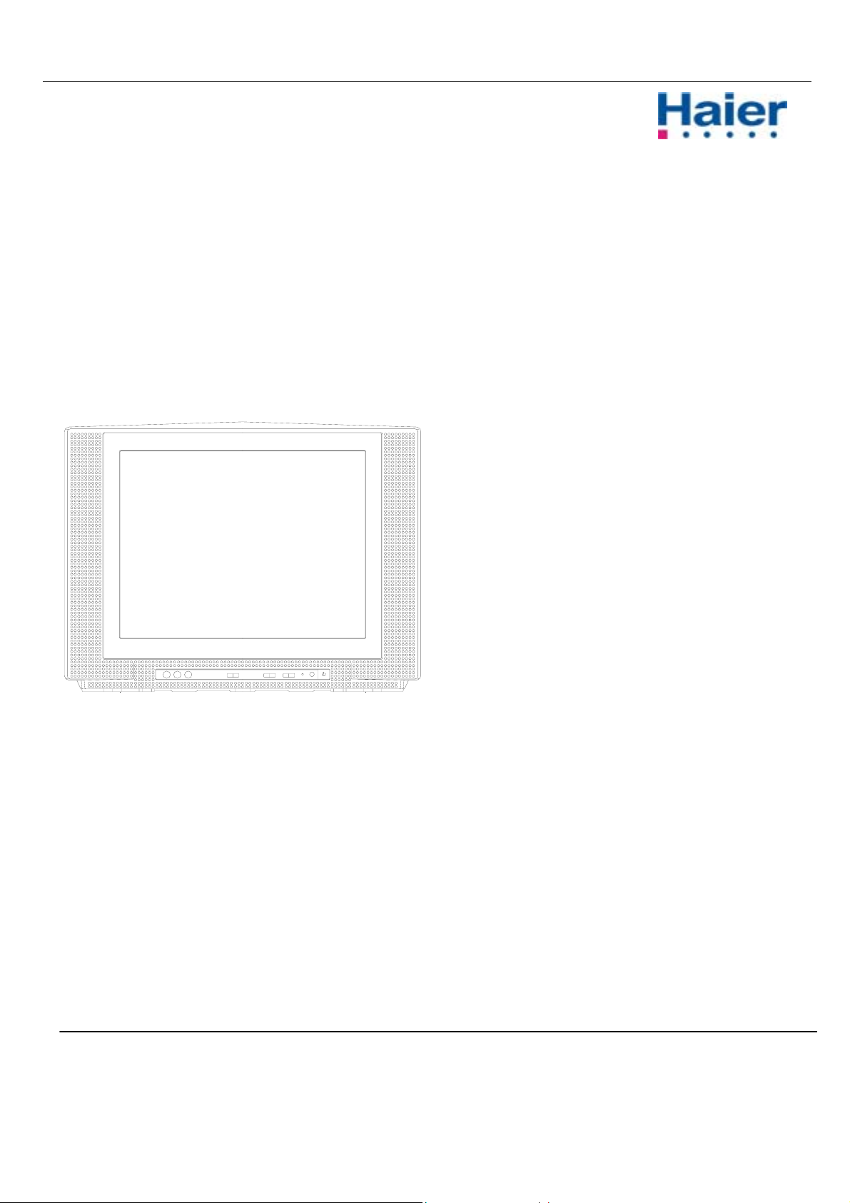
HT
X21S31
COLOR TELEVISION
Service Manual
MODEL: HTX21S31
Haier
Features
PAL M/N, NTSC M
Front Audio/Video input
V-CHIP, CCD
181 Channel
Haier Group
NO:M-LA-EC-2199-76812 -Edition: 2002.12.30
Page 2

CONTENTS
CONTENTS
1 Contents--------------------------------------------------------------------1
2 Product Code illumination and Series Introduction--------------------2
3 Features--------------------------------------------------------------------------------3
4 Safety Precautions------------------------------------------------------------------4
5 Warning and Cautions-------------------------------------------------------------5
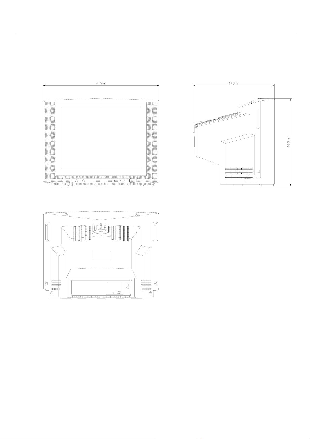
6 Net dimension----------------------------------------------------------------------11
7 Parts and Functions--------------------------------------------------------------12
8 Remote Controller Functions--------------------------------------------------13
9 Program Diagram------------------------------------------------------------------14
10 Maintenance Service and Trouble shooting------------------------------15
11 Circuit Diagram---------------------------------------------------------------------18
12 Circuit Explanation----------------------------------------------------------------22
13 Adjustment---------------------------------------------------------------------------24
14 Exploded View----------------------------------------------------------------------27
15 List of Parts--------------------------------------------------------------------------28
16
Damageable Parts List-----------------------------------------------------------41
17
Information of Resistors and Capacitors----------------------------------41
1
Page 3
Product Code illumination and Series Introduction
2.
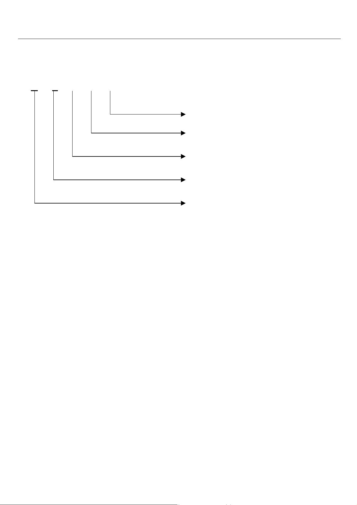
Product Code illumination and Series Introduction
T X 21 S31
H
Color television appearance
CRT size (unit: inch)
Toshiba
Haier
2
Page 4
Features
3.
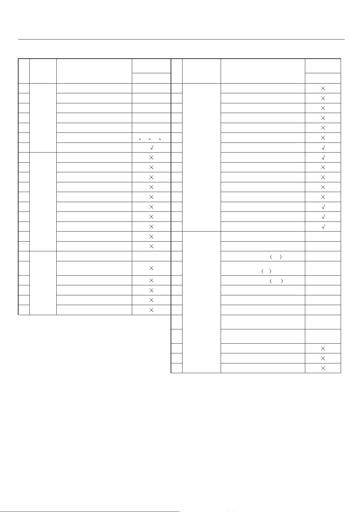
Features
PICTURE
1
2
3
4
5
6
7
AUDIO
8
9
10
11
12
13
14
15
16
17
18
19
20
21
22
23
ITEM
JACK
NO.
FUNCTION
Main IC 76814
CRT
Color system
Audio system
Number of channels
OSD language
Multi-picture modes
AV stereo
Super woofer
Surrounding sound
Treble/bass boost
Left/right balancer
NICAM
Multi-audio modes
Tone adjuster
MTS/SAP
Auto-volume leveling
AV input
AV output
DVD terminal
S-video jack
Headphone socket
SCART socket
Flat square 25
E
MODEL
HTX21S31
NTSC 26
M 27
181 28
F S P
Front 1 41
NO.
24
29
30
31
32
33
34
35
36
37
38
39
40
42
43
44
45
46
47
48
49
50
51
ITEM
SOFTWARE
PARAMETER
FUNCTION
Digital curtain
Slow fading on & off
Semitransparent menu
Non-flashing channel changing
ZOOM
16:9 mode
Games
Calendar
Child-lock
Multi-functional lock
No-picture listening
Background light
Auto-timer on
CCD
V-CHIP
Number of built-in speakers
Audio output power (W)
Total power input W
Voltage range
Power frequency
Time of sleep timer (MINS)
Net weight (KG)
Gross weight (KG)
Net dimension (MM)
Packaged dimension (MM)
Quantity for 20' container
Quantity for 40' container
Quantity for 40' high container
V
Hz
MODEL
HTX21S31
2
2
70
90VAC-250V
AC
60
120
23.5
25
610X475X46
5
685X545X52
0
3
Page 5

Safety Precautions
4.
Safety Precautions
SAFETY PRECAUTIONS
IMPORTANT SAFETY NOTICE
Many electrical identify these parts and mechanical parts in this chassis have special safety-related
characteristics! In the Schematic Diagram and Replacement Parts List.
It is essential that these special safety parts should be replaced with the same components as
recommended in this manual to prevent X-RADIATION, Shock, Fire, or other Hazards.
Do not modify the original design without permission of the manufacturer.
General Guidance
An Isolation Transformer should always be used during the servicing of a receiver whose chassis is
not isolated from the AC power line. Use a transformer of adequate power rating as this protects the
technician from accidents that might result in personal injury caused by electrical shocks.
It will also protect the receiver and it’s components from being damaged by accidental shorts of the
circuitry that might be inadvertently introduced during the service operation.
If any fuse (or Fusible Resistor) in this TV receiver is blown, replace it with a specified one.
When replacing a high wattage resistor (Oxide Metal Film Resistor, over 1W), keep the resistor
10mm away from PCB.
Keep wires away from high voltage or high temperature parts.
Due to the high vacuum and large surface area of the picture tube, extreme care should be taken in
handling the Picture Tube. Do not lift the Picture Tube by its Neck.
X-RAY Radiation
Warning:
The source of X-RAY RADIATION in this TV receiver is the High Voltage Section and the Picture
Tube.
For continued X-RAY RADIATION protection, the replacement tube must be of the same type as
specified in the Replacement Parts List.
Before returning the receiver to the customer,
Always perform an AC leakage current check on the exposed metallic parts of the cabinet, such as
antennas, terminals, etc., to make sure that the set is safe to operate without any danger of electrical
shock.
4
Page 6
g
Warning and Cautions
5.
Warning and Cautions
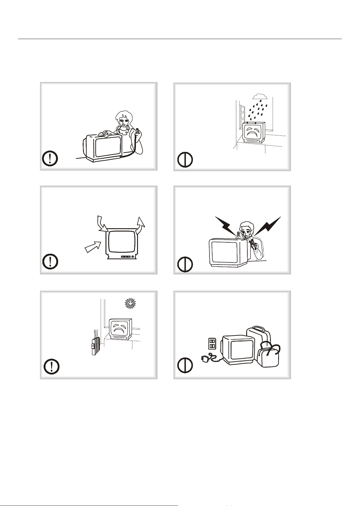
1. When you clean the TV set, please pull
out the power plu
clean the cabinet and the screen with
benzene, petrol and other chemicals.
from AC outlet. Don't
2.
In order to prolong the using life of the
TV set, please place it on a ventilated
place.
4. To prevent the TV set from firing and
electric shock, don't
make the TV set rain
or moisture.
5. Don't open the back cover, otherwise it is
possible to damage the components in the
TV set and harm you.
3.
Don't place the
TV set in the
sunshine or near
heat source.
6. When the TV set isn't going to be used
for long time or it is in thunder and
lightening, please pull out the pl ug from AC
outlet and the antenna plug from the cover
of the TV set.
Explanation on the display tube
Generally, it is not needed to clean the tube surface. However, if necessary,its surface can be
cleaned with a dry cotton cloth after cutting off the power.Don't use any cleanser. If using hard
cloth, the tube surface will be damaged.
CAUTION: Before servicing receivers covered by this service manual and its supplements and
addenda, read and follow the SAFETY PRECAUTIONS.
5
Page 7

Warning and Cautions
NOTE: If unforeseen circumstances create conflict between the following servicing precautions and
any of the safety precautions, always follow the safety precautions. Remember: Safety First.
General Servicing Precautions
1). Always unplug the receiver AC power cord from the AC power source before:
a. Removing or reinstalling any component, circuit board module or any other assembly of the
receiver.
b. Disconnecting or reconnecting any receiver electrical plug or other electrical connection.
c. Connecting a test substitute in parallel with an electrolytic capacitor in the receiver.
CAUTION: A wrong substitution part or incorrect installation polarity of electrolytic capacitors
may result in an explosion hazard.
d. Discharging the picture tube anode.
2). Test high voltage only by measuring it with an appropriate high voltage meter or other
voltage-measuring device (DVM, FETVOM, etc.) equipped with a suitable high voltage probe. Do not
test high voltage by “drawing an arc”.
3) .Discharge the picture tube anode only by (a) first connecting one end of an insulated clip lead to
the degaussing or kine aquadag grounding system shield at the point where the picture tube socket
ground lead is connected, and then (b) touch the other end of the insulated clip lead to the picture
tube anode button, using an insulating handle to avoid personal contact with high voltage.
4) .Do not sprays chemicals on or near this receiver or any of its assemblies.
5). Unless specified otherwise in this service manual, clean electrical contacts only by applying the
following mixture to the contacts with a pipe cleaner, cotton-tipped stick or comparable nonabrasive
applicator; 10% (by volume) Acetone and 90% (by volume) isopropyl alcohol (90%-99% strength)
CAUTION: This is a flammable mixture.
Unless specified otherwise in this service manual, lubrication of contacts is not required.
6). Do not defeat any plug / socket B+ voltage interlocks with which receivers covered by this
service manual might be equipped.
7). Do not apply AC power to this instrument and/or any of its electrical assemblies unless all
solid-state device heat sinks are correctly installed.
8) Always connect the test receiver ground lead to the receiver chassis ground before connecting
the test receiver positive lead.
Always remove the test receiver ground lead last.
9). Use with this receiver only the test fixtures specified in this service manual.
CAUTION: Do not connect the test fixture ground strap to any heat sink in this receiver.
Electrostatic ally Sensitive (ES) Devices
Some semiconductor (solid state) devices can be damaged easily by static electricity. Such
6
Page 8

Warning and Cautions
components are usually called Electrostatic ally Sensitive (ES) Devices. Examples of typical ES
devices are integrated circuits and some field effect transistors and semiconductor “chip”
components. The following techniques should be used to help reduce the incidence of component
damage caused by static electricity.
1) Immediately before handling any semiconductor component or semiconductor- equipped
assembly, drain off any electrostatic charge on your body by touching a known earth ground.
Alternatively, obtain and wear a commercially available discharging wrist strap device, which should
be removed to prevent potential shock prior to applying power to the unit under test.
2) After removing an electrical assembly equipped with ES devices, place the assembly on a
conductive surface such as aluminum foil, to prevent electrostatic charge buildup or exposure of the
assembly.
3) Use only a grounded-tip soldering iron to solder or unsolder ES devices.
4) Use only an anti-static type folder removal device. Some solder removal devices not classified as
“anti-static” can generate electrical charges sufficient to damage ES devices.
5) Do not use freon-propelled chemicals. These can generate electrical charges sufficient to
damage ES devices.
6) Do not remove a replacement ES device from its protective package until immediately before you
are ready to install it. (Most replacement ES devices are packaged with leads electrically shorted
together by conductive foam, aluminum foil or comparable conductive material).
7) Immediately before removing the protective material from the leads of a replacement ES device,
touch the protective material to the chassis or circuit assembly into which the device will be installed.
CAUTION: Be sure no power is applied to the chassis or circuit, and observe all other safety
precautions.
8) Minimize bodily motions when handling unpackaged replacement ES devices. (Otherwise even
some normally harmless motions such as mutual brushing of your clothes’ fabric or lifting of your
foot from a carpeted floor might generate static electricity sufficient to damage an ES device.)
General Soldering Guidelines
1) Use a grounded-tip, low-wattage soldering iron and appropriate tip size and shape that will
maintain tip temperature within the range of 500 oF to 600 oF.
2) Use an appropriate gauge of RMA resin-core solder composed of 60 parts tin/40 parts lead.
3) Keep the soldering iron tip clean and well tinned.
4) Thoroughly clean the surfaces to be soldered. Use a mall wire bristle (0.5 inch, or 1.25cm) brush
with a metal handle. Do not use freon-propelled spay-on cleaners.
5) Use the following unsoldering technique
a. Allow the soldering iron tip to reach normal temperature. (500 o F to 600o F)
b. Heating the component lead until the solder melts.
c. Quickly draw the melted solder with an anti-static, suction-type solder removal device with
solder braid.
7
Page 9

Warning and Cautions
CAUTION: Work quickly to avoid overheating the circuit board printed foil.
1) Use the following unsoldering technique
a. Allow the soldering iron tip to reach normal temperature. (500 o F to 600o F)
b. First, hold the soldering iron tip and solder the strand against the component lead until the
solder melts.
c. Quickly move the soldering iron tip to the junction of the component lead and the printed
circuit foil, and hold it there only until the solder flows onto and around both the component
lead and the foil.
CAUTION: Work quickly to avoid overheating the circuit board printed foil.
d. Closely inspect the solder area and remove any excess or splashed solder with a small
wire-bristle brush.
Remove /Replacement
Some chassis circuit boards have slotted holes (oblong) through which the IC leads are inserted and
then bent flat against the circuit foil. When holes are of slotted type, the following technique should
be used to remove and replace the IC. When working with boards using the familiar round hole, use
the standard technique as outlined.
Removal
Desolder and straighten each IC lead in one operation by gently prying up on the lead with the
soldering iron tip as the solder melts.
Draw away the melted solder with an anti-static suction-type solder removal device (or with solder
braid) before removing the IC.
Replacement
Carefully insert the replacement IC in the circuit board.
Carefully bend each IC lead against the circuit foil pad and solder it.
Clean the soldered areas with a small wire-bristle brush. (It is not necessary to reapply acrylic
coating to the areas).
“Small-Signal” Discrete Tr ansistor
Removal/Replacement
Remove the defective transistor by clipping its leads as close as possible to the component body.
Bend into a “U” shape the end of each of three leads remaining on the circuit board.
Bend into a “U” shape the replacement transistor leads.
Connect the replacement transistor leads to the corresponding leads extending from the circuit board
and crimp the “U” with long nose pliers to insure metal to metal contact then solder each connection.
Power Output, Transistor Device
Removal/Replacement
Heat and remove all solder from around the transistor leads.
8
Page 10

Warning and Cautions
Remove the heat sink mounting screw (if so equipped).
Carefully remove the transistor from the heat sink of the circuit board.
Insert new transistor in the circuit board.
Solder each transistor lead, and clip off excess lead.
Replace heat sink.
Diode Removal/Replacement
Remove defective diode by clipping its leads as close as possible to diode body.
Bend the two remaining leads perpendicularly to the circuit board.
Observing diode polarity, wrap each lead of the new diode round the corresponding lead on the
circuit board.
Securely crimp each connection and solder it.
Inspect (on the circuit board copper side) the solder joints of the two “original” leads. If they are not
shiny, reheat them and if necessary, apply additional solder.
Fuse and Conventional Resistor
Removal/Replacement
1) Clip each fuse or resistor lead at top of the circuit board hollow stake.
2) Securely crimp the leads of replacement component around notch at stake top.
3) Solder the connections
CAUTION: Maintain original spacing between the replaced component and adjacent components
and the circuit board to prevent excessive component temperatures.
Circuit Board Foil Repair
Excessive heat applied to the copper foil of any printed circuit board will weaken the adhesive that
bonds foil to the circuit board causing the foil to separate from or “lift-off” the board. The following
guidelines and procedures should be followed whenever this condition is encountered.
At IC Connections
To repair a defective copper pattern at IC connections use the following procedure to install a jumper
wire on the copper pattern side of the circuit board. (Use this technique only on IC connections).
1) Carefully remove the damaged copper pattern with a sharp knife. (Remove only as much copper
as absolutely necessary).
2) Carefully scratch away the solder resist and acrylic coating (if used) from the end of the remaining
copper pattern.
3) Bend a small “U” in one end of a small gauge jumper wire and carefully crimp it around the IC pin.
Solder the IC connection.
4) Route the jumper wire along the path of the out-away copper pattern and let it overlap the
previously scraped end of the good copper pattern. Solder the overlapped area and clip off any
excess jumper wire.
9
Page 11

At other connections
Use the following technique to repair the defective copper pattern at connections other than IC Pins.
This technique involves the installation of a jumper wire on the component side of the circuit board.
1) Remove the defective copper pattern with a sharp knife.
Remove at least 1/4 inch of copper, to insure that a hazardous condition will not exist if the jumper
wire opens.
2) Trace along the copper pattern from both sides of the pattern break and locate the nearest
component that is directly connected to the affected copper pattern.
3) Connect insulated 20-gauge jumper wire from the lead of the nearest component on one side of
the pattern break to the lead of the nearest component on the other side.
Carefully crimp and solder the connections.
CAUTION: Be sure the insulated jumper wire is dressed so that it does not touch components or
sharp edges.
Warning and Cautions
10
Page 12
6.Net dimension
Net dimension
Haier
11
Page 13
TV/AV MENU
P
10
1. C able TV Antenna Hookup
11
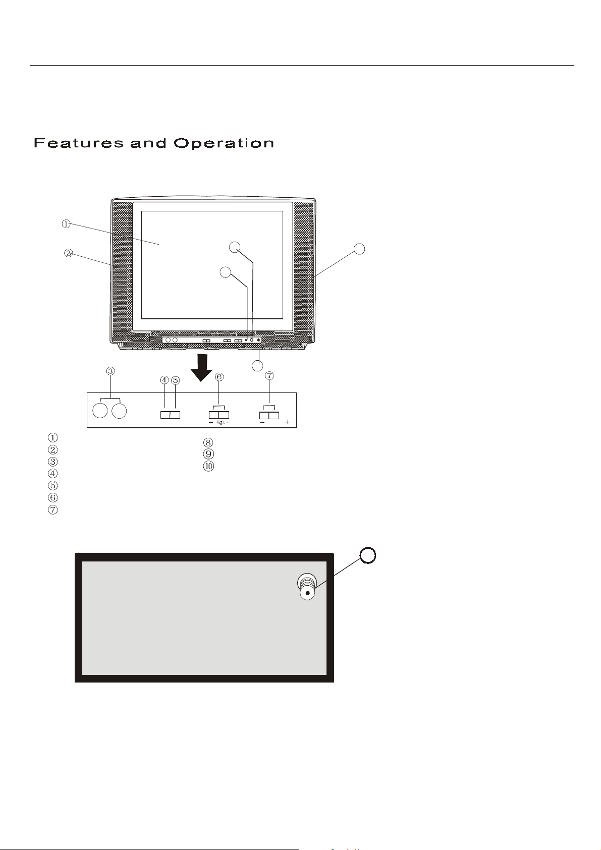
7.Parts and Functions
Parts and Functions
1.Front Panel
Picture Tube
Left Speaker
input
AV
HTX21S31 TV
TV/AV alteration button
Menu button
Volume up/down button
Channel up/down button
9
8
Front
Audio (R) input
Power indicator
Power switch
11.Right speaker
TV Rear Panel
1
ANT
12
Page 14
8.Remote Controller Functions
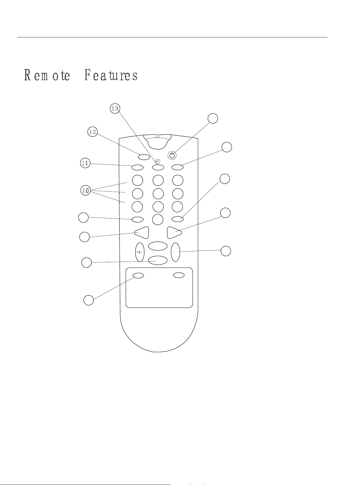
Remote Controller Functions
1
2
TV/AV
1 2 3
DISP
3
654
7 8 9
9
SOUN D
0
M ENU RECALL
RATING
4
8
CH+
VO L+
7
P.S TD
CH-
SYS
5
6
1. Power Button
2. Tim e & Channel D is p la y B u tto n
3. Rat ing Button
TV Pr ogr am ( V- Chip Setup)
4. Last Channel R e c a ll Button
5. Volum e( +/ - ) Select But t on
6. Per sonal Preference Select
7. Channel ( +/ - ) Select But ton
13
8. Menu Select Button
9. Audio Select Button
10.D irect Access Channel Select
11 . TV/AV Input But ton
12. M ute Butt on
13. Sleep Tim er
14.SYSTEM s elec tion
Page 15

Program Diagram
Program Diagram
9.
Insert the power plug into the power line socket and insert the antenna plug into the antenna socket
on the rear panel. Press down the power switch of the TV set. The red indicator light goes on.
Program preset
A 1). Auto searching and storing program
Press MENU button on the remote controller to call up the “PREST” menu on the screen. Use the
“ ” key to select the bar “auto search” then press the “ ” to make sure. If you want to stop,
press the key “ ”.
2). Deleting channel number
Press channel up/down buttons to select a channel to skip. Press MENU to call up the “PREST”
menu on the screen. Then Press the” “item to select the bar “Add/Delete”
then use the “ ” key to select Add or Delete.
B Volume tuning
Press VOLUME buttons VOL- to decrease and VOL+ to increase the volume.
C Personal preference settings
Picture modes
Press P.STD repeatedly to change among Personal, Stadard, Vvivid, Soft to change the Picture Mode.
14
Page 16
.
10.Maintenance service and trouble shooting
Maintenance service and trouble shooting
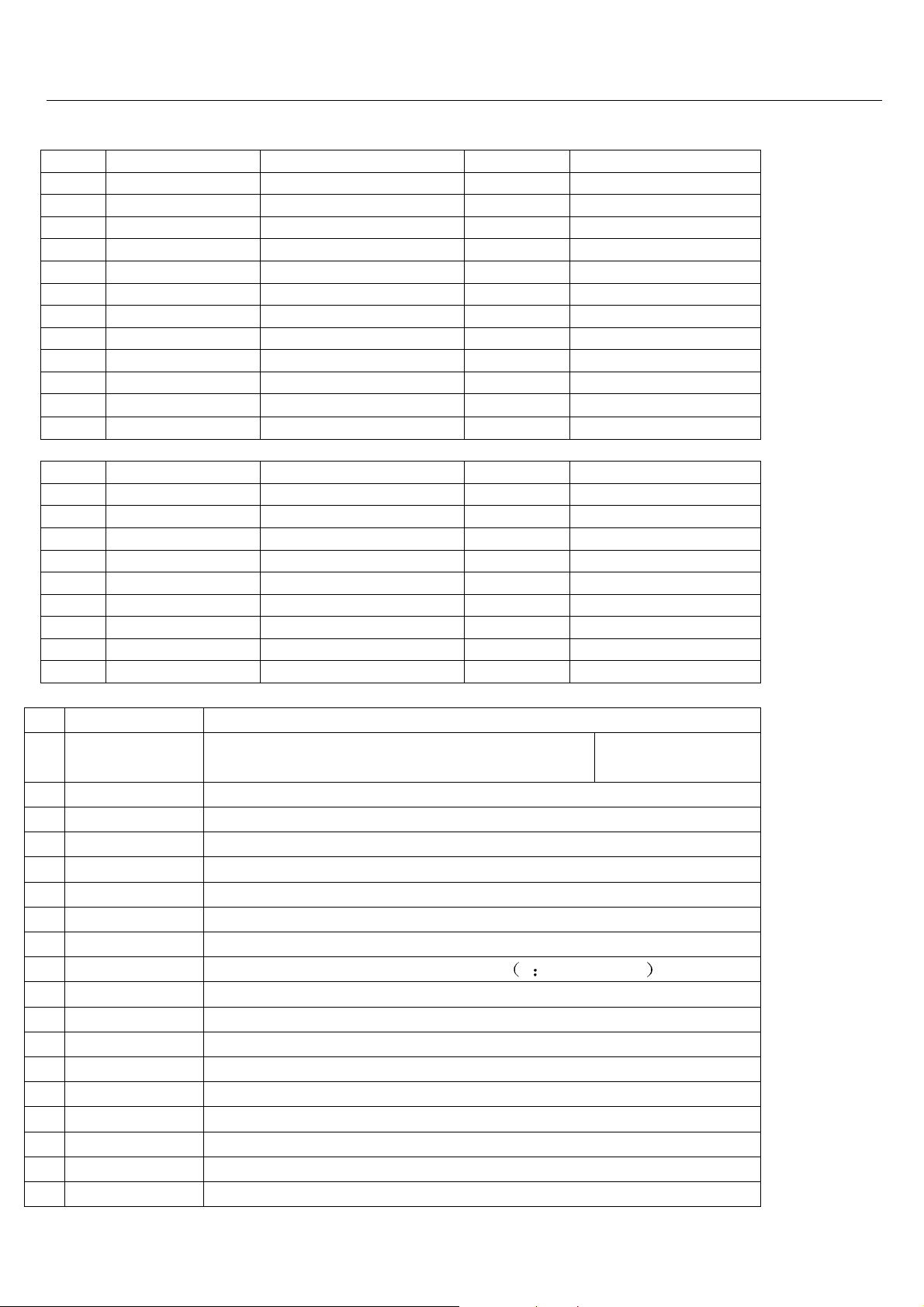
1). Adjustment item Explanation:
OSD Explanation Range Remark
0 H.PHASE H.PHASE 0~31
1 NT.H.PHASE H.PHASE 0~31 No used
2 H.BLK.LEFT 0~7
3 H.BLK.RIGHT 0~7
4 V.SIZE Vertical Size 0~127
5 V.LINE Vertical Linearity 0~31
6 V.POSI Vertical DC 0~63
7 V.SC Vertical S-Correction 0~31
8 NT.V.SIZE Vertical Size -32~+31
9 NT.V.LINE Vertical Linearity -16~+15
10 NT.V.POSI Vertical DC -32~+31
11 NT.V.SC Vertical S-Correction -16~+15
12 RF.AGC RF AGC Delay 0~63
13 VOL.OUT Volume Control 0~127
14 OSD H.POSI 0~127
15 OSD V.POSI 0~31
16 INPUT LEVEL 0~15
17 SPECTRAL 0~63 (0~31)PHILIP IC
18 WIDEBAND 0~63 (0~31)PHILIP IC
19 STEREO VCO 0~63 No used
20 FILTER SET 0~63 No used
21 SAP VCO 0~63 No used
2). Setting item explanation:
OSD Function
0 LA76814/LA768
0: select LA76814 1:select LA76812
12
1 SAP IC SELECT 0:TDA9850;1:CXA2104;2:TDA9855;3:UPC1815B
2 SUB.CONT Sub-contrast(0-31)
3 SUB.COLOR Sub-color(0-63)
4 SUB.SHARP Sub-sharpness(0-31)
5 SUB.TINT Sub-tint(0-63)
6 BLK.STR.DEF Black level stretch (0:on; 1:off)
7 AFC GAIN AFC gain (0:low; 1:high)
8 V.SEPUP Vertical synchronize sensitive 0 low;1:high
9 CD.MODE “Count down mode”(LA76814:0/1;LA76812:0-7)
10 DIGITAL OSD Digital OSD setting (0:anlyos 1:digital)
11 OSD CONT. OSD contrast (0-127)/LA76814 (0-3)
12 GRAY MOD Gray mode (0/1)
13 B.GAM.SEL Blue γ select (0-3)
14 RG.GAM.DEF Red green γ define (0/1)
15 FBPBLK.SW FBPBLK.SW (0/1)
16 BRIGHT ABL.TH “Bright.abl.threshold”(0-7)
17 EMG.ABL.DEF “Emg.abl.def”
15
Page 17
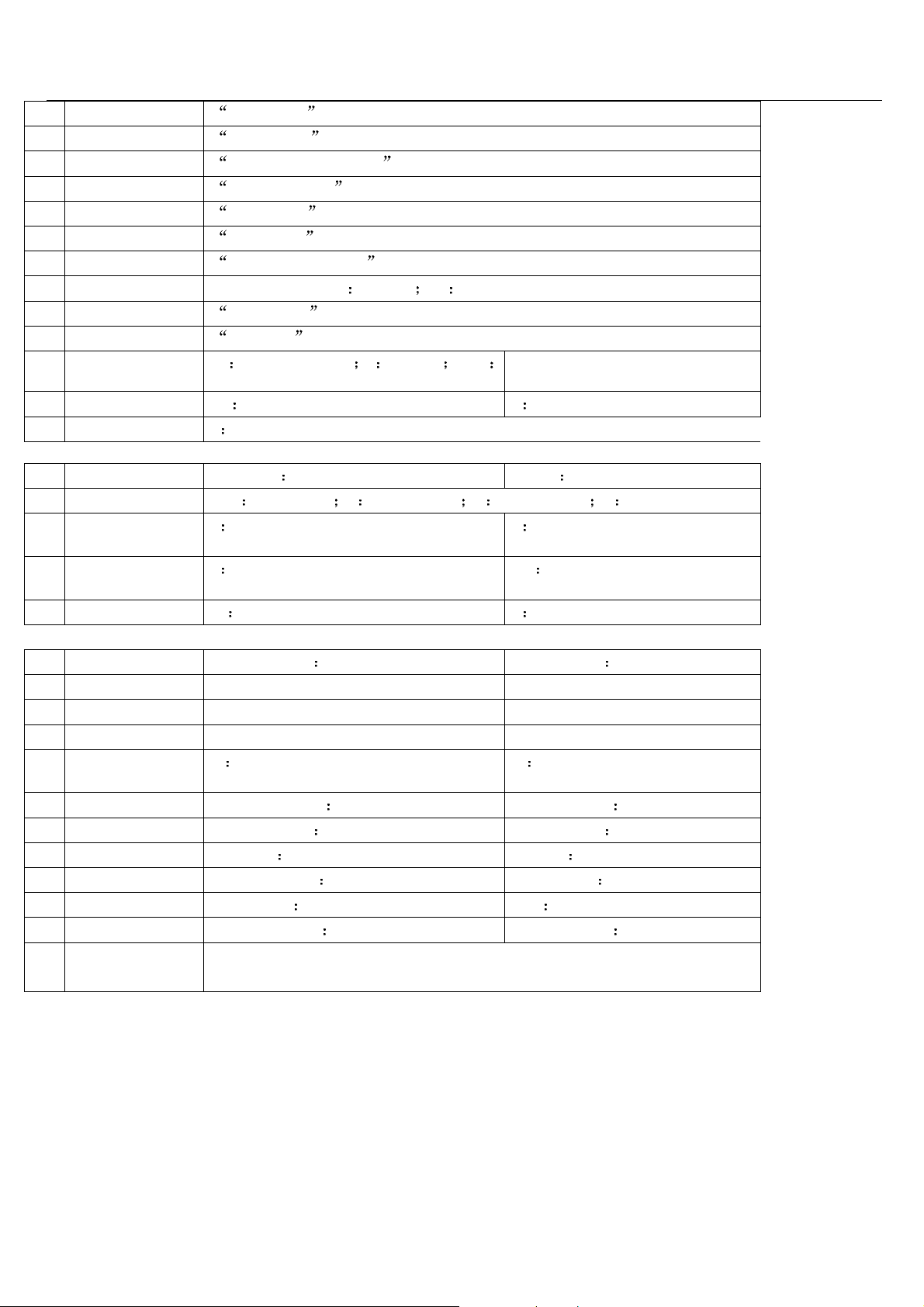
Maintenance service and trouble shootin
g
18 BRT.ABL.DEF
19 MID.STP.DEF
20 R—Y/B-Y G.BL
21 R-Y/B-Y ANG
22 C.KILL.OFF
23 SND.TRAP
24 VOL.FIL
25 VIF.SYS.SW
26 VIDEO.LELEVL
27 FM.LEVEL
28 POWER OPT
29 POWER FLAG
30 SEARCH CHECK
31 SEARCH SPEED
32 AV OPTION
33 POSITION L/R
34 BLUE BACK
35 BLACK BACK
Brt.Abl.Def (0/1)
Mid.Stp.Def (0/1)
R-Y/B-Y Gain Balance (0~15) No use (LA76814)
R-Y/B-Y Angle (0~15)
C_Kill OFF (0/1)
Sound Trap (0~7)
Volume Filter Defeat
Video IF setting (0 45.75M 1 58.75M) For LA76814
Video Level (0~7)
FM Level (0~31)
0 turn TV on twice 1 memory 2或3
Turn TV on first
0 Without OSD power on function 1 With OSD power off function
1 With auto-programmed function turning TV on.
0 Slow search speed 1 Fast search speed
0 without AV 1 one AV input 2 two AV input 3 Three AV input
0 Logo display on left top of screen 1 Logo display on right top of
0 No blue background without signal 1 Blue background without
0 No background changing channel 1 Background changing channel
.
screen
signal
36 STEREO OPTION
37 WOOF/H.PHONE
38 WOOF VOL.OPT
39 SENSITIVITY
40 V.MUTE P.OFF
41 CCD OPTION
42 V-CHIP OPTION
43 PASSWORD OPT.
44 COMB.OPTION
45 TUNER OPTION
46 GAME OPTION
0 Before POWER OFF, don’t cut off
0 No stereo 1 Stereo
No used
No used
No used
video input
0 No CCD 1 CCD
0 No V-CHIP 1 V-CHIP
0 No V-CHIP password 1 V-CHIP password
0
NOTHING
0 TDF-3M3 tuner 1 PHILIP UV1336B tuner
0 No game 1 Game
1 Before POWER OFF, cut off
1
No used
No used
No used
video input
NOTHING
47 SCREEN OPTION 0:no curtain effect 1: curtain for on effect 2:curtain for off
effect 3:curtain for on/off effect
16
Page 18
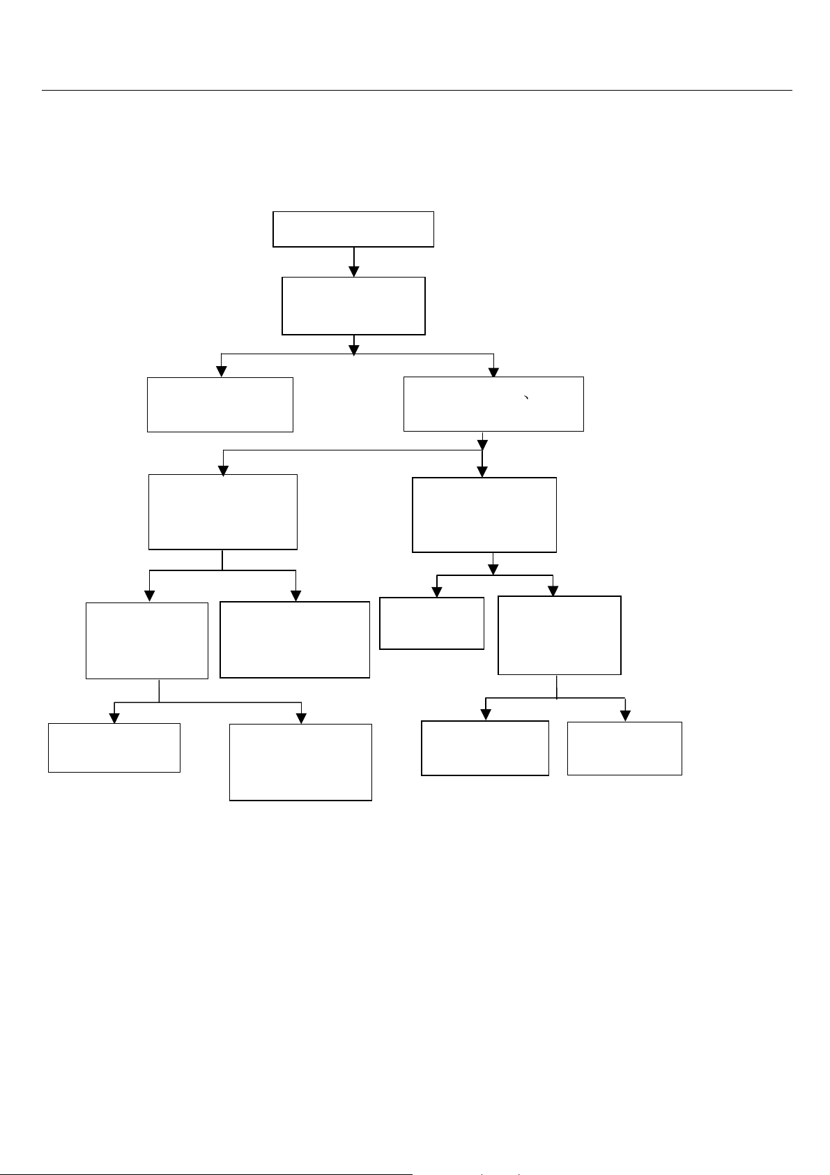
p
A
Maintenance Service and Trouble shooting
No lig
Normal
Check N101
Normal
Check to see
if , 12v,
5v is normal
Normal
Check VD501, C507,
V513, etc.
Check to see if the
collector voltage of V552
is 0V
Check the control
voltage of V552 or
CPU power
The failure of
horizontal unit or
N551 N552
Check to see if
Fuse3 is normal
Normal
Abnormal
Abnormal
Normal
Check
ower unit
Normal
Abnormal
Check to see 110V 180V
etc. voltage is normal
bnormal
Test to see all terminal
Resistance of load
Is normal
Change
rectifying tube
Check to see if
rectifying tube
Abnormal
is normal
Abnormal
Check the
Loader
17
Page 19

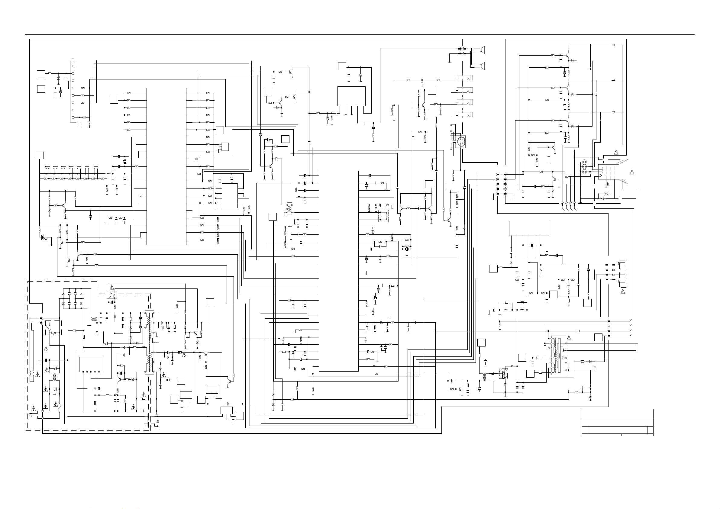
11. Circuit Diagram
Circuit Diagram
18
Page 20
R727
1/6W470
L909
LJ0107CHA
AC110V
60HZ
U902
EW0130KB
B1
110V
B7
5V
B5
5V
1/6W1.5K
VD701
BT205-L
R700
1/6W10K
R722
1
2
C532
AC400V470
R718
2W10K
16V100
SW701
CH+
XS501
TJC2-2A
00
0
L501
JLB1606
1
2
N706
UPC574
C101
+
SW702
CH-
R701
1/6W27K
R723
1/6W8.2K
VD703
HZ4A2
1/6W4.7K
R728
1/6W470
VD503
RM11C
VD504
RM11C
00
0
C502
AC250V0.1U
C501
AC250V0.1U
R501
1/2W220K
FU501
T2.5A250V
C708
50V4.7
C102
63V0.01U
SW703
V+
R702
1/6W8.2K
R724
V703
2SC1815
V705
2SC1815
C503
1KV1000
C504
1KV1000P
RT501
PTH451A7R0Q21
A101
UV1336B
IF
33V
+
5V
R101
5V
R104
1/6W100
SCL
R105
1/6W100
SDA
NC
1/6W1K
AGC
+
SW705
SW704
MENU
V-
R703
R704
1/6W4.7K
1/6W3.9K
R720
1/6W10K
V702
2SA1015
R731
R734
1/6W10K
1/6W10K
R721
1/6W10K
V704
2SC1815
R733
1/4W8.2K
C505
1KV1000
C506
1KV1000P
R502
6W1
LIVE AREA
1/6W33K
R103
C103
16V2.2
SW706
X
R705
1/6W2.7K
VD505
RM11C
VD506
RM11C
R515
2W68K
R102
1/6W100K
R706
1/6W1.5K
C729
63V0.01U
R729
1/6W150K
R730
1/6W10K
L503
JLB1606
VD507
IN4148
R504
0.1
SW707
POWER
R732
1/6W47K
C507
450V150
C513
2KV330
R707
1/6W680
C554
1KV470
C518
1KV1000
+
L504
YC0008
L701
39UH
1/6W10K
4
R506 680
B5
5V
+
R708
R726
1/6W270K
C714
16V2.2
C510
470
C705
63V18P
C704
63V15P
C701
16V47
C703
63V0.01U
R725
1/6W330
+
C713
50V1
21
3
N501
HPC922
R566
1/6W10K
VD555
ES1
R513
1M
R514
1M
R510
C513
470
V501
2SA1015
R508
1/6W4.7K
VD508 1N4148
C511
1000
G701
32.768K
YC0008
VD511
EU2
VD510
EU2
10K
1/6W10K
1/6W22K
1/6W22K
C702
63V0.01U
+
R515
2W68K
VD512
EG01C
L505
R509
10K
R765
1/6W22K
R746
1/6W22K
R748
1/6W22K
R735
R750
R752
R511
8.2
VD509
HZ15C
R507
1/6W1.5K
R709
1/6W390K
T511
BCK-40-58
C515
0.022
C516
0.022
L506
YC0008
R502
6W1
1/2CK5.6M
C533
AC400VM2200
G2R-1A
3
2
R531
RL551
1
2
3
4
5
6
7
8
9
10
11
12
13
14
15
16
17
18
19
20
21
3
NOTHING
NOTHING
NOTHING
NOTHING
NOTHING
NOTHING
POWER
VT
GND
XTAL1
XTAL2
VDD
KEY IN
AFT IN
AGC IN
NC
RESET
FILT
CVBS-IN
V SYNC
H SYNC
N701
LC86F3248A
10
9
8
11
12
14
13
VD551
C561
RU3A
160V220
C551
2KV470
C554
1KV470
VD554
EU2Z
VD555
ES1
RSG-I-FF-125V-750mA
C565
+
25V1000
VD553
1N4148
R562
Circuit Diagram
B901
XP601
XS601
TJC3-2A
C612
16V10
+
R612
1/6W470
B2
17V
+
N601
LA4225A
NON INPUT
INPUT
1
2
SIF APC FIL
SIF OUT
EXT AUDIO IN
VCO FIL
VCO COIL
VCO COIL
APC FIL
VIDEO OUT
BLK STRETCH FIL
INT VIDEO IN
VCC (V/C/D)
EXT VIDEO IN
GND (V/C/B)
SEL VIDEO OUT
APC1 FIL
FSC OUT
APC2 FIL
KILL FLT
GND (CCD/H)
OSD CONTRAST
VCC (CCD)
CLOCK OUT
VCO IREF
C616
25V1000
GND
3
SIF IN
XTAL
X-RAY
FBP IN
OUT
4
C617
63V0.01U
VCC
5
C613
25V1000
+
54
53
52
51
50
49
48
47
46
45
44
43
42
41
40
39
38
37
36
35
34
33
32
31
30
C279
63V0.01U
29
28
C614
X
C126
63V39
C123
63V1000
C140
63V470
R128
X
R201
1/6W1K
C204
50V1
C205
63V0.01U
100V0.01
R271
1K
+
C412
50V1
+
C276
16V10
1/6W3K
R273
1/4W4.7K-J
+
R272
R613
C124
100V0.01
+
C137
50V0.47
C207
C207
100V0.01
16V47
R409
1/6W680
X
+
C139
50V0.47
R204
1/6W560K
G201
4.43
R414
1/6W10K
C278
R121
1/6W1K
+
+
+
C206
16V47
C208
50V0.47
VD412
HZ7C1
+
1/6W56K
R127
1/6W330
+
R413
1/6W10K
R803
C801
16V10
T101
HA6019
C203
16V4.7
R270
J
R206
1/6W47K
1/6W22K
R412
1/6W8.2K
R415
1/6W3.9K
R271
1/6W150
C277
100V0.01
+
R202
1/6W1.2K
R205
R805
R814
X
+
R806
V802
X
R804
1/6W82
R810
1/6W75
B6
12V
R807
1/6W220
B6
12V
R811
1/6W75
C804
16V470
1/6W1K
R808
X
R809
X
V801
2SC1815
R832
+
R818
XS801-1
AUDIO
XS802-1
VIDEO
XS801-2
X
XS802-2
X
W807
J
Y
C
XS802
X
R817
X
B7
C808
5V
X
R815
X
R816
X
R819
X
X
V803
X
VD801
R820
X
X
C807
X
C431
X
R432
J
V431
2SC2383-O
R801
1/6W22K
C809
2200
R812
X
C805
X
+
R813
X
R802
1/6W100
C802
+
16V10
C821
+
50V1
1/6W27K
V821
2SC1815
C803
16V10
R821
1/6W4.7K
1/6W68K
R822
1/6W1K
R203
1K
L201
15UH
Z201
X4.5
C411
VD411
+
25V47
EU1
R604
1/6W4.7K
V603
+
R113
1/6W100K
R114
1/6W100K
VD401
R602
1/6W10K
V601
2SA1015
C603
16V100
B6
12V
1/6W270
+
C401
50V0.47
R400
1/4W270
+
C408
50V1
R119
1/6W1K
Z101
LBN45U
38M
L102
15UH
R241
1/6W100
R242
1/6W100
R243
C402
63V0.22U
R403
1/6W330K
2SC1815
C117
50V1
C244
+
16V47
R401
1/6W2.2K
+
C404
16V220
100V0.068U
+
C407
50V1
V602
2SC1815
100V0.022U
C115
+
16V100
+
R244
1/6W2.7K
C403
63V0.47U
C406
R402
1/6W3.3K
R404
1/6W1.2K
+
C122
63V0.01U
C121
100V0.022U
C120
C119
63V0.01U
C116
63V0.01U
R120
J
C118
63V0.01U
C245
63V0.01U
C405
63V0.01U
C601
16V10
R611
1/6W3.3K
C611
100V0.022U
N101
LA76812
1
AUDIO OUT
2
FM OUT
3
PIF AGC
4
RF AGC
5
VIF IN1
6
VIF IN2
7
GND(IF)
8
VCC (VIF)
9
FM FIL
10
AFT OUT
11
DATA
12
CLOCK
13
ABL
14
R IN
15
G IN
16
B IN
17
BLANK IN
18
VCC (RGB)
19
R OUT
20
G OUT
21
B OUT
22
AKB IN
23
V OUT
24
RAMP ALC.FIL
25
VCC (H)
26
H AFC FIL
27
H OUT
R408
1/6W2.2K
+
C604
16V100
R764
NOTHING
41
NOTHING
40
AV/TV
39
AV1
38
AV2
37
NOTHING
36
NOTHING
35
SIF
34
IR
33
SD
32
S-VHS
31
SAFTY
30
SCL1
29
SDA1
28
SCL0
27
SDA0
26
I
25
BLANK
24
B OUT
23
G OUT
22
R OUT
R556
1/6W22K
R555
1/2W47K
R551
2WJ47K
+
R552
1/2W100K
RP551
2AL2K
B1-ADJ
R553
1/6W4.7K
R569
1/2W 1
+
C564
25V1000
B2
17V
N553
AN7805
B5
5V
+
C570
10V470
1/6W22K
V553
2SC1815
123
R756
1/6W10K
R566
1/6W10K
R754
1/6W3.3K
1/6W4.7K
VD561
HZ6C3
R567
1/6W1.2K
N551
AN7812
B6
12V
1/6W22K
R762
1/6W22K
1/6W22K
1/6W22K
1/6W2.2K
R758
1/6W22K
1/6W22K
1/6W1K
1/6W22K
1/6W22K
R742
R740
1/6W4.7K
R738
R736
1/6W4.7K
R554
1/6W150K
R763
R761
R760
R759
R757
R766
R755
R753
1/6W22K
R751
1/6W22K
R749
1/6W22K
R747
B1
110V
V554
2SB892
123
N552
AN7805
B5
5V
A701
HS0038
C719
+
16V47
1
2
3
4
R743
1/6W3.3K
R741
X
R739
X
R737
X
123
N702
BR24C04
W405
EU2Z
10V470
C572
C720
63V0.01U
VCC
GND
SCL
SDA
1/6W10K
V552
2SC1815
+
R745
1/6W220
R561
B7
5V
8
7
6
5
1/6W22K
42
R744
1/6W220
R109
1/6W1K
B6
12V
R601
1/6W10K
C110
63V0.01U
C111
63V0.01U
R108
1/6W5.6K
V102
2SC2216
R111
1/6W82
B7
5V
VD601
1N4148
R107
1/6W100
R110
1/6W220
C112
63V0.01U
1N4148
VD402
1N4148
SCN3-2Y
R433
1/2W1K
C433
500V3900
3W16OHM
B902
3W16OHM
B1
110V
R434
5W3.3K
T431
JDT1904
C432
500V1000
+
C434
160V10
B4
24V
C441
200V0.33U
L431
YC0008
XS403
SCN-5
L451
18UH
+
V432
2SD1651
L432
YC0008
XP902
SCN-5Y
C451
35V100
VD451
EM01Z
R442
L442
101K
C444
160V4.7
R446
1/4W220K
CRT BOARD
5
4
3
2
1
N451
LA7840
PUMP OUT
7
+
C452
35V1000
1/6W5.6K
L433
ZZ0003
C435
1.6KV7500
R451
VCC2
6
+
1/2W1K
INPUT
R441
L441
Z0449
B4
24V
C436
2KV470
C931
+
16V10
5
C453
63V1000
35V100
R931
1/6W1K
R932
15K
R933
1/6W1.5K
16V1000
NON INPUT
4
C455
63V10P
+
C454
50V1
R454
1/6W3K
+
C472
B1
110V
ABL
C933
VCC1
VD472
EU1
1/6W10K
+
3
H-PULSE
R471
6W3.9
16V10
R900
R935
39
C934
50V0.47
OUTPUT
2
R453
1/6W12K
C450
16V100
R472
1W1
R904
1/6W330
R914
1/6W330
R924
1/6W330
C932
GND
R452
1/6W1
VD452
1Z75
1
+
1/6W100
+
+
9
4
10
1
2
R902
1/6W100
C903
63V56
R912
1/6W100
C913
63V56P
R922
C923
63V56P
SCN-4Y
C459
100V0.1U
R455
1/6W12K
B6
12V
JF0501-19129
9
4
C901
63V390
63V390
63V390
V931
2SA1015
V932
2SC1815
VD933
1N4148
XP901
T471
C911
C921
R456
1/6W12K
1
R459
1W1
R907
R908
1/2W2.7K
R918
1/2W2.7K
R928
1/2W2.7K
XS901
GZS8-6-4F
11
8
9
10
5
C939
2KV1000
11
XS402
8
TJC2-5A
9
4
10
3
2
1
XS401
SCN-4Y
3
2
B3
180V
4
3
2
C474
+
250V22
1
C231
50V1
HT-2199(LA76812)
3
2
NTSC-M PAL-M,N
HR76814
2W10K
R917
2W10K
R927
2W10K
W902 JG0034
71
K6D
5
XP402
TJC2-5Y
V902
2SC2688
VD901
1N4148
R906
1/6W560
V912
2SC2688
VD911
1N4148
R916
1/6W680
V922
2SC2688
VD921
1N4148
R926
1/6W680
K9N
TJC2-1A
R940
1/4W33
2
34
R460
1/2W180
C458
100V0.033U
R457
1/6W39K
+
+
C457
C456
35V1000
50V4.7
2
1
3 4
R458
R461A
1/6W1K
1/2W120
B4
12V
R491
1W2.2
HV
FO
SCREEN
VD474
R474
1W1
EU1
TP-H
R233
TEST
1/2W1.5K
R232
1/6W10K
Title
Size Document Number Rev
Date: Sheet of
TP-G
TEST
8
7 1
U901
XXXXXXX
FO
1
11Tuesday, March 12, 2002
NO:M-LA-EC-2199-76812 -Edition: 2002.12.30
Page 21
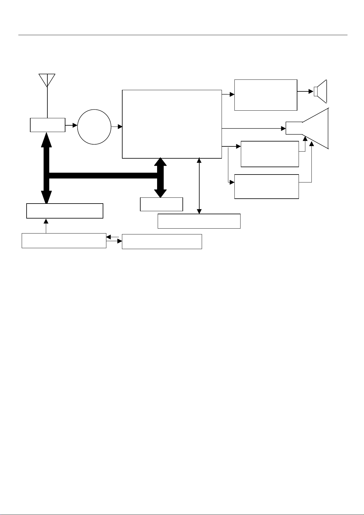
Circuit Block Diagram
Circuit Block Diagram
Tune
Antenna
r
I2C BUS
SAW
Picture/Sound IF Amplifier,
Video and audio signal
Processing,
RGB Output Circuits
and H &V Sync pulse
segregation
Sound Power
Amplifier
CRT
Horizontal Scan
Output
Vertical Scan
Output
Main Processor
Infrared Receiver
Remote Controller
ROM
Audio/Video In/Out
NO:M-LA-EC-2199-76812 -Edition: 2002.12.30
Page 22
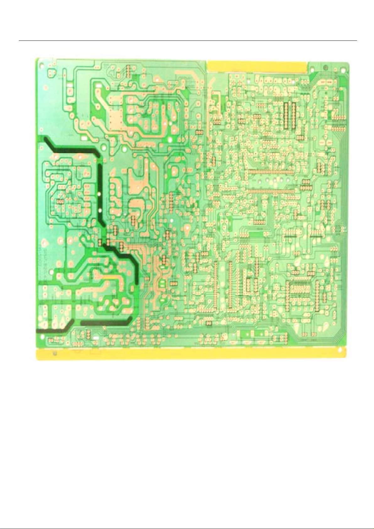
PCB
21
Page 23
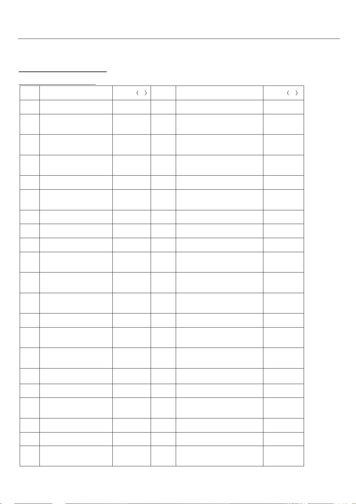
Circuit Explanation
12. Circuit Explanation
IC reference data:
1). N701 (LC86F3232A)
Pin
No.
function
voltage
V
1 n.c 22 R-input 0.06
Connect to 5V via a
2
5.03 23 G-input 0.06
resistor
Connect to 5V via a
3
5.03 24 B-input 0.07
resistor
Connect to 5V via a
4
5.04 25 Blank 0.15
resistor
5 Connect to 5V via a 5.03 26 n.c. 0.01
Connect to 5V via a
6
5.03 27 I2C bus control 0 4.85
resistor
Pin
No.
function
voltage V
7 standby 0.03 28 I2C bus control 0 4.79
8 n.c. 0 29 I2C bus control 1 5
9 Ground 0 30 I2C bus control 1 4.99
Connect to 5V via a
10 Scl 1.47 31
5.03
resistor
Connect to 5V via a
11 sdl 2.2 32
5.04
onnect to 5V via a resisto
Connect to 5V via a
12 Power supply 4.99 33
5.03
resistor
13 Key input 0.24 34
遥控接收
0.03
Connect to 5V via a
14 AFT in 2.77 35
5.02
resistor
Connect to 5V via a
15 AGC in 1.7 36
5.01
resistor
16 n.c. 1.7 37 mute 0.11
17 Reset 4.99 38 AV select 0.02
Connect to 5V via a
18 Filter 3.13 39
5.02
resistor
19 CVBS in 3.25 40 Connect to 5V via a resist 5.01
20 V syn input 4.8 41 C resistor 5.01
Connect to 5V via a
21 H syn input 4.12 42
5.02
resistor
22
Page 24
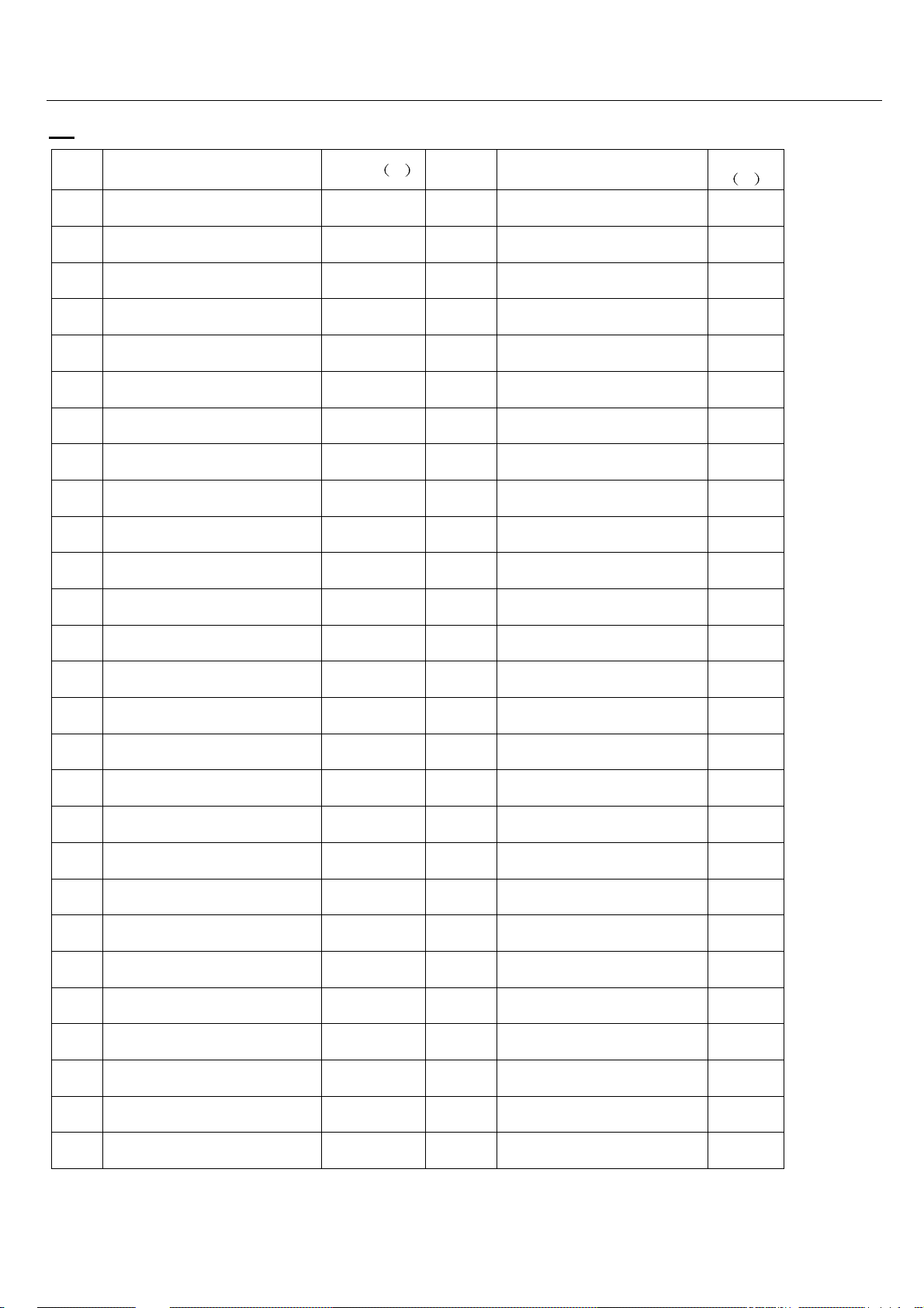
2). N101 LA76812
Circuit Explanation
Pin
No.
function
voltage
V
Pin
No.
function
voltage
V
1 Audio output 2.23 28 FBT input 1.06
2 FM output 2.23 29 VCO IREF 1.69
3 IF AGC filter 2.22 30 Clock output 0.002
4 RF AGC 2.59 31 VCC 0.002
5 PIF AMP input 1.30 32 OSD gain control 3.05
6 PIF AMP input 2.83 33 Gnd 0
7 IF ground 2.83 34 X-ray pretect 0.06
8 IF VVcc 0 35 ACC killer filter 0.39
9 FM filter 4.94 36 APC2 filter 3.49
10 AFT output 1.90 37 FSCout 0.54
11 Bus data 2.77 38 XTAL 2.87
12 Bus clock 4.85 39 APC1 filter 3.2
13 ABL 4.76 40 Selected video output 2.43
14 R-input 3.92 41 Video chroma deflection 0
15 G-input 0.14 42 Ext video input 2.55
16 B-input 0.15 43 Power 5
17 Fast blanking input 0.08 44 Int . video input 2.77
18 RGB Vcc 7.94 45 Black stretch filter 2.6
19 R-output 2.21 46 Video input 2.12
20 G-output 2.36 47 APC filter 3.5
21 B-output 2.28 48 VCO coil 4.3
22 H-synchronize output 0 49 VCO coil 4.3
23 Vertical output 2.47 50 FLL filter 2.24
24 Vertical ramp ALC filter 2.65 51 Ext audio input 2.12
25 Power 5.10 52 SIF output 1.95
26 AFC filter 2.49 53 APC filter 2.38
27 Horizontal output 0.63 54 SIF input 3.14
23
Page 25

13. Adjustment
IF alignment:
1). Test equipment:
a. 45.75MHz sweep generator
b. 15V/3A DC power supply (with short and over current proof)
c. Digital multi-meter d. If alignment tool
f. User Remote controller g. Service remote controller
h. Video signal generator i. Multi-system adjustment tool
j. 60MHz double trace oscillograph(2 units)
k. White balance adjustment instrument
2). Signal, power supply connection:
a.Connect +15V DC power supply to the +15V testing top in the main PCB.
b.Input sweep signal into IF testing top
c.Connect multi-meter to PIF-TP testing top in PCB.
3). Alignment
a.Connect 45.75MHz sweep generator to IF test top in PCB
b.Adjust T101 and make digital multi-meter display 3.6V±0.05V.
(PIF-TP top can only connect to multi-meter).
Adjustment
Alignment and check:
a. Connect main PCB with alignment tool, input factory adjustment signal, and turn TV
on. Adjust screen control on FBT and make screen brightness relevant receive 525-line
monoscope, adjust focus control on FBT and make focus relevant.
b. Pre-adjust power voltage: adjust RP551 and make +B voltage be 109V±0.5V.
c. Check brightness, contrast, color, and sharpness: receive color bar signal and adjust
contrast, brightness, color, sharpness control, picture will change accordingly.
d. AV input check: press AV/TV button, screen will display AV mode or TV mode and audio
input signal can be observed, picture and sound must be normal.
optimal.
S
24
Page 26
Main power adjustment:
Adjustment: Connect voltage meter to +B on main PCB, make +B voltage be 110V±0.3V.
Adjustment
Screen voltage adjustment:
Adjustment: Tune TV on, receive a digital test pattern, set brightness and contrast standard
mode. Press “FACTORY” button on the service remote controller twice,”B/W balance display on
the screen, then press “MUTE” button, and make a horizontal bright line display on the screen.
Adjust Screen voltage of FBT, make the line just seen. Then press “MUTE” button and exit service
mode. Press “P.STD” button and make picture enter standard mode.
AGC ALIGNMENT:
Receive a color bar signal, 60dB,NTSC M color bar pattern, and check if there is noise in the picture, if there is
noise, press FACTORY button and enter service mode, adjust RF.AGC value and make the noise just disappear,
press FACTORY button and exit service mode.
White balance adjustment:
Turn TV on, receive white field signal, and make the probe of white balance adjustment instrument touch with
top and bottom of screen fully. Check if values of R, G, B are standard, if not, press “FACTORY” button, make
“B/W BALANCE” menu display on screen, adjust values of R-BIA, G-BIA, B-IA, R-DRV, G-DRV, B-DRV,
make them standard. Press FACTORY button, exit service mode.
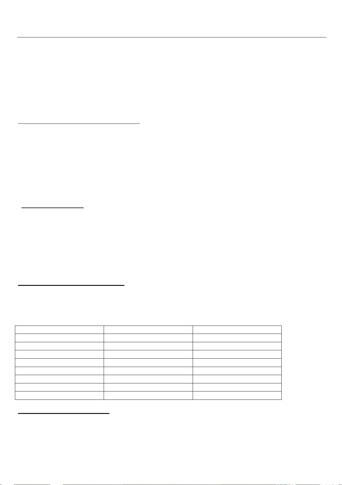
OSD I2C bus control (LA76810) Varied range
S-BRI Sub brightness 0-127
R-BIA Red bias 0-255
G-BIA Green bias 0-255
B-BIA Blue bias 0-255
R-DRV Red drive 0-127
G-DRV Green drive 0-15
B-DRV Blue drive 0-127
C.B/W Cross B/W 0-3
FOCUS ALIGNMENT
Receive crosshatch (N system) pattern; Adjust focus-variable resistor on the FBT, make picture is the
sharpest.
25
Page 27

Adjustment
GEOMETRIC ALIGNMENT:
Receive the monochrome circle pattern (NTSC system);
Check vertical center and horizontal center and H-linearity .if they are not standard, press FACTORY button to
enter service mode, and adjust vertical size, vertical linearity, vertical center, horizontal center, make them
standard.
Alignment parameter table:
Press FACTORY button on service remote controller and enter service mode: 1.Adjustment mode and2.
Setting mode;
Use CH+ or CH- button up/down pages to select items that you need adjust; use
VOL+ or VOL- button
26
 Loading...