

Page 1
SERVICE MANUAL
LCD TV
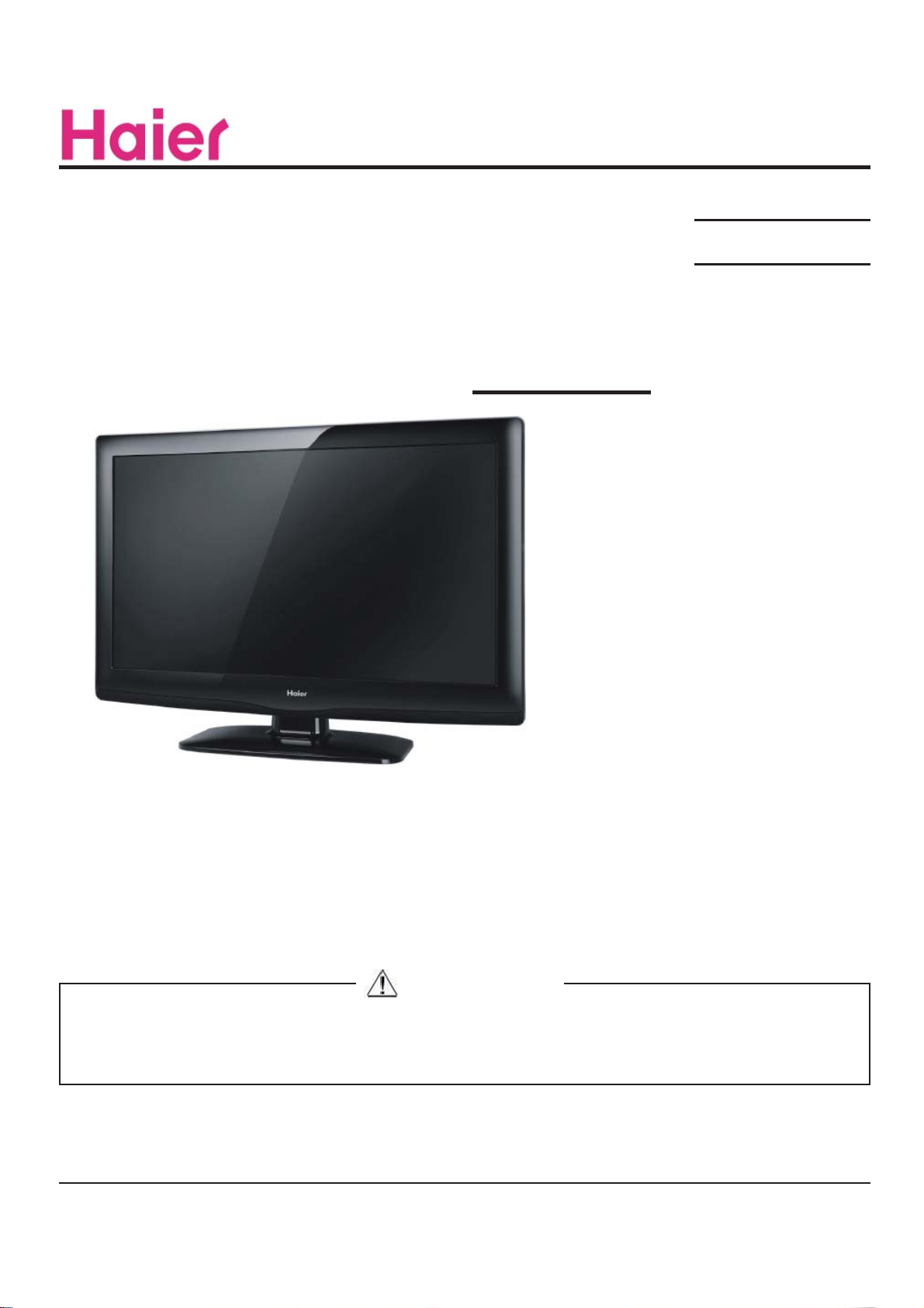
Model No. HL19KN2
TSUMV26KU
Chassis
WARNING
This service information is designed for experienced repair technicians only and is not designed for use by the general public.
It does not contain warnings or cautions to advise non-technical individuals of potential dangers in attempting to service a product.
Products powered by electricity should be serviced or repaired only by experienced professional technicians. Any attempt to service or repair
the product or products dealt with in this service information by anyone else could result in serious injury or death.
©2009 Qingdao Haier Electronics Co., Ltd.
All rights reserved. Unauthorized copying and distribution is a violation of law.
Haier Group
Page 2

Service Manual
Model No.:
Chapter 1: General Information
1-1. Table of Contents
1. General Information...........................................................................
1-1. Table of Contents
1-2. General Guidelines
1-3. Important Notice
1-4. How to Read this Service Manual
2. Specifications....................................................................................
3. Location of Controls and Components...........................................
3-1. Board Location
3-2. Main Board & AV Board
3-3. Power Board
3-4. LCD Panel
4. Disassemble and Assemble..........................................................
4-1 Remove the Pedestal
4-2 Remove the Back Cover 15
4-3 Remove the Adhesive Tape 15
4-4 Remove the Terminal Bracket
1
4
4
4
7
7
88
8
8
11
12
15
15
16
4-5 Remove the Power Module 16
4-6 Remove the Main Board 16
4-7 Remove the Speaker 17
4-8 Remove the Remote Control Board 17
5. Installation Instructions..…....………………...........………….........
5-1 External Equipment Connections 18
5-2 HDMI Connections 21
6. Operation Instructions....…....………………...........………….........
6-1 Front Panel Controls
6-2 Back Panel Controls
6-3 Universal Remote Control
7. Electrical Parts…....………………...........………….........................
7-1. Block Diagram
7-2. Circuit Diagram
7-3. Wiring Connection Diagram
8. Measurements and Adjustments........…………............................
18
24
24
24
25
26
26
27
36
37
- 01 -
Page 3

Service Manual
Model No.:
9. Trouble-shooting…………..............................................................
9-1. Simple Check 39
9-2. Main Board Failure Check
9-3. Panel Failure
39
40
41
- 02 -
Page 4

Service Manual
Model No.:
1-2. General Guidelines
When servicing, observe the original lead dress. If a short circuit is found, replace all parts
which have been overheated or damaged by the short circuit.
After servicing, see to it that all the protective devices such as insulation barriers, insulation
papers shields are properly installed.
After servicing, make the following leakage current checks to prevent the customer from
being exposed to shock hazards.
1) Leakage Current Cold Check
2) Leakage Current Hot Check
3) Prevention of Electro Static Discharge (ESD) to Electrostatically Sensitive
1-3. Important Notice
1-3-1. Follow the regulations and warnings
Most important thing is to list up the potential hazard or risk for the service personnel to
open the units and disassemble the units. For example, we need to describe properly
how to avoid the possibility to get electrical shock from the live power supply or charged
electrical parts (even the power is off).
This symbol indicates that high voltage is present inside.It is dangerous to
make any king of contact with any inside part of this product.
This symbol indicates that there are important operating and maintenance
instructions in the literture accompanying the appliance.
1-3-2. Be careful to the electrical shock
To prevent damage which might result in electric shock or fi re, do not expose this TV set
to rain or excessive moisture. This TV must not be exposed to dripping or splashing water,
and objects fi lled with liquid, such as vases, must not be placed on top of or above the TV.
1-3-3. Electro static discharge (ESD)
Some semiconductor (solid state) devices can be damaged easily by static electricity. Such
components commonly are called Electrostatically Sensitive (ES) Devices. The following
techniques should be used to help reduce the incidence of component damage caused by
electros static discharge (ESD).
1-3-4. About lead free solder (PbF)
This product is manufactured using lead-free solder as a part of a movement within the
consumer products industry at large to be environmentally responsible. Lead-free solder
must be used in the servicing and repairing of this product.
1-3-5. Use the genewing parts (specifi ed parts)
Special parts which have purposes of fire retardant (resistors), high-quality sound
(capacitors), low noise (resistors), etc. are used.
When replacing any of components, be sure to use only manufacture's specified parts
shown in the parts list.
Safety Component
● Components identifi ed by mark have special characteristics important for safety.
- 03 -
Page 5

Service Manual
Model No.:
1-3-6 Safety Check after Repairment
Confi rm that the screws, parts and wiring which were removed in order to service are put
in the original positions, or whether there are the positions which are deteriorated around
the serviced places serviced or not. Check the insulation between the antenna terminal or
external metal and the AC cord plug blades. And be sure the safety of that.
General Servicing Precautions
1. Always unplug the receiver AC power cord from the AC power source before;
a. Removing or reinstalling any component, circuit board module or any other receiver
assembly.
b. Disconnecting or reconnecting any receiver electrical plug or other electrical
connection.
c. Connecting a test substitute in parallel with an electrolytic capacitor in the receiver.
CAUTION: A wrong part substitution or incorrect polarity installation of electrolytic
capacitors may result in an explosion hazard.
2. Test high voltage only by measuring it with an appropriate high voltage meter or other
voltage measuring device (DVM, FETVOM, etc) equipped with a suitable high voltage
probe.
Do not test high voltage by "drawing an arc".
3. Do not spray chemicals on or near this receiver or any of its assemblies.
4. Unless specified otherwise in this service manual, clean electrical contacts only by
applying the following mixture to the contacts with a pipe cleaner, cotton-tipped stick or
comparable non-abrasive applicator; 10% (by volume) Acetone and 90% (by volume)
isopropyl alcohol (90%-99% strength).
CAUTION: This is a fl ammable mixture.
Unless specifi ed otherwise in this service manual, lubrication of contacts is not required.
Capacitors may result in an explosion hazard.
5. Do not defeat any plug/socket B+ voltage interlocks with which receivers covered by this
service manual might be equipped.
6. Do not apply AC power to this instrument and/or any of its electrical assemblies unless
all solid-state device heat sinks are correctly installed.
7. Always connect the test receiver ground lead to the receiver chassis ground before
connecting the test receiver positive lead.
Always remove the test receiver ground lead last. Capacitors may result in an explosion
hazard.
8. Use with this receiver only the test fi xtures specifi ed in this service manual.
CAUTION: Do not connect the test fi xture ground strap to any heat sink in this receiver.
9. Remove the antenna terminal on TV and turn on the TV.
10. Insulation resistance between the cord plug terminals and the eternal exposure metal
should be more than Mohm by using the 500V insulation resistance meter.
11. If the insulation resistance is less than M ohm, the inspection repair should be required.
If you have not the 500V insulation resistance meter, use a Tester. External exposure
metal: Antenna terminal Headphone jack
- 04 -
Page 6

Service Manual
Model No.:
Electrostatically Sensitive (ES) Devices
Some semiconductor (solid-state) devices can be damaged easily by static electricity.
Such components commonly are called Electrostatically Sensitive (ES) Devices.
Examples of typical ES devices are integrated circuits and some field-effect transistors
and semiconductor "chip" components. The following techniques should be used to help
reduce the ncidence of component damage caused by static by static electricity.
1. Immediately before handling any semiconductor component or semiconductorequipped assembly, drain off any electrostatic charge on your body by touching a known
earth ground. Alternatively, obtain and wear a commercially available discharging wrist
strap device, which should be removed to prevent potential shock reasons prior to applying
power to the unit under test.
2. After removing an electrical assembly equipped with ES devices, place the assembly
on a conductive surface such as aluminum foil, to prevent electrostatic charge buildup or
exposure of the assembly.
3. Use only a grounded-tip soldering iron to solder or unsolder ES devices.
4. Use only an anti-static type solder removal device. Some solder removal devices not
classifi ed as "anti-static" can generate electrical charges suffi cient to damage ES devices.
5. Do not use freon-propelled chemicals. These can generate electrical charges suffi cient
to damage ES devices.
6. Do not remove a replacement ES device from its protective package until immediately
before you are ready to install it.
(Most replacement ES devices are packaged with leads electrically shorted together by
conductive foam, aluminum foil or comparable conductive material).
7. Immediately before removing the protective material from the leads of a replacement
ES device, touch the protective material to the chassis or circuit assembly into which the
device will be installed.
CAUTION: Be sure no power is applied to the chassis or circuit, and observe all other
safety precautions.
8. Minimize bodily motions when handling unpackaged replacement ES devices.
(Otherwise harmless motion such as the brushing together of your clothes fabric or the
lifting of your foot from a carpeted fl oor can generate static electricity suffi cient to damage
an ES device.)
1-3-7. Ordering Spare Parts
Please include the following informations when you order parts. (Particularly the Version
letter)
1. Model number, Serial number and Software Version
The model number and Serial number can be found on the back of each product and the
Software Version can be found at the Spare Parts List.
2. Spare Part No. and Description
You can fi nd them in the Spare Parts List
- 05 -
Page 7

1-3-8. Photo used in this manual
The illustration and photos used in this Manual may not base on the final design of
products, which may differ from your products in some way.
1-4. How to Read this Service Manual
Using Icons:
Icons are used to attract the attention of the reader to specifi c information. The meaning of
each icon is described in the table below:
Note:
A “note” provides information that is not indispensable, but may nevertheless be valuable
to the reader, such as tips and tricks.
Service Manual
Model No.:
Caution:
A “caution” is used when there is danger that the reader, through incorrect manipulation,
may damage equipment, loose data, get an unexpected result or has to restart(part of) a
procedure.
Warning:
A “warning” is used when there is danger of personal injury.
Reference:
A “reference” guides the reader to other places in this binder or in this manual, where he/
she will fi nd additional information on a specifi c topic.
- 06 -
Page 8
Service Manual
Model No.:
2. Specifications
Model HL19KN2
Screen Size 19 inch
Aspect Ratio 16:9
Resolution 1366x768
Response Time (ms)
Angel of View 176 C
Color Display 16777216
No. of Preset Channels 125
OSD Language English
Color System NTSC
Audio System M,N
Audio Output Power
(Built-in) (W)
Audio Output Power
(outer) (W)
Total Power Input (W) 30W
Voltage Range (V) AC100V-240V
Power Frequency (Hz) 50~60Hz
Net Weight (KG) 4
8 (GRAY TO
GRAY)
1.5W×2
No
Gross Weight (KG) 4.8
Net Dimension (MM) 460x140x346
Packaged Dimension
541x171x408
(MM)
- 07 -
Page 9
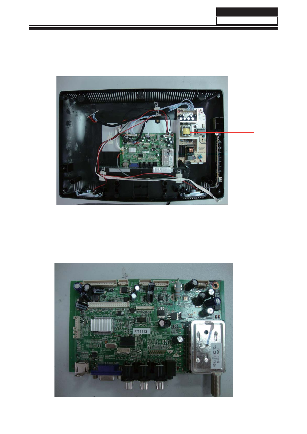
3. Location of Controls and Components
3-1 Board Location
Service Manual
Model No.:
B Board
A Board
3-2 Main Board
- 08 -
Page 10
Service Manual
Model No.:
3-2-1 Function Description:
Main Board
Process signal which incept from exterior equipment then translate into signal that panel
can display.
3-2-2 Connector defi nition
Main board connector
Power connectors (J10, J2)
J10
J2
Pin number Signal name Pin number Signal name
1 +5V 1 GND
2 BL 2 GND
3 DIM 3 +5V
4
high voltage
4 +5V
5 GND 5 POWER ON/OFF
6 +5VSTB
7 +5V
8 +5V
9 GND
10 GND
11 GND
12 +12V
13 +12V
Notes:
J10-Pin 2: Backlight on/off:
The system can turn on or turn off the backlight of TFT LCD Panel through the power
supply unit path.
J2-Pin 5: System power on / standby
System board will use this pin to control system power.
J10-Pin 3: Control the luminance of backlight
The system can generate the PWN signal to control the strength of TFT LCD Panel’s
backlight through this connector
- 09 -
Page 11
Service Manual
Model No.:
remote connector (J6)
Pin number Signal name Description
1 LED_R LAMP RED
2 LED_G LAMP GREEN
3
4 IR REMOTE CONTROL
5 GND GND
6 5V POWER FOR REMOTE
Keypad and connector (J7)
Pin number Signal name Description
1 KEY1
2 KEY0
3 GND
- 10 -
Page 12
Service Manual
Model No.:
Speaker connector J11
Pin number Signal name Description
1 RSPK+ RSPK+
2 RSPK- RSPK-
3 LSPK- LSPK 4 LSPK+ LSPK+
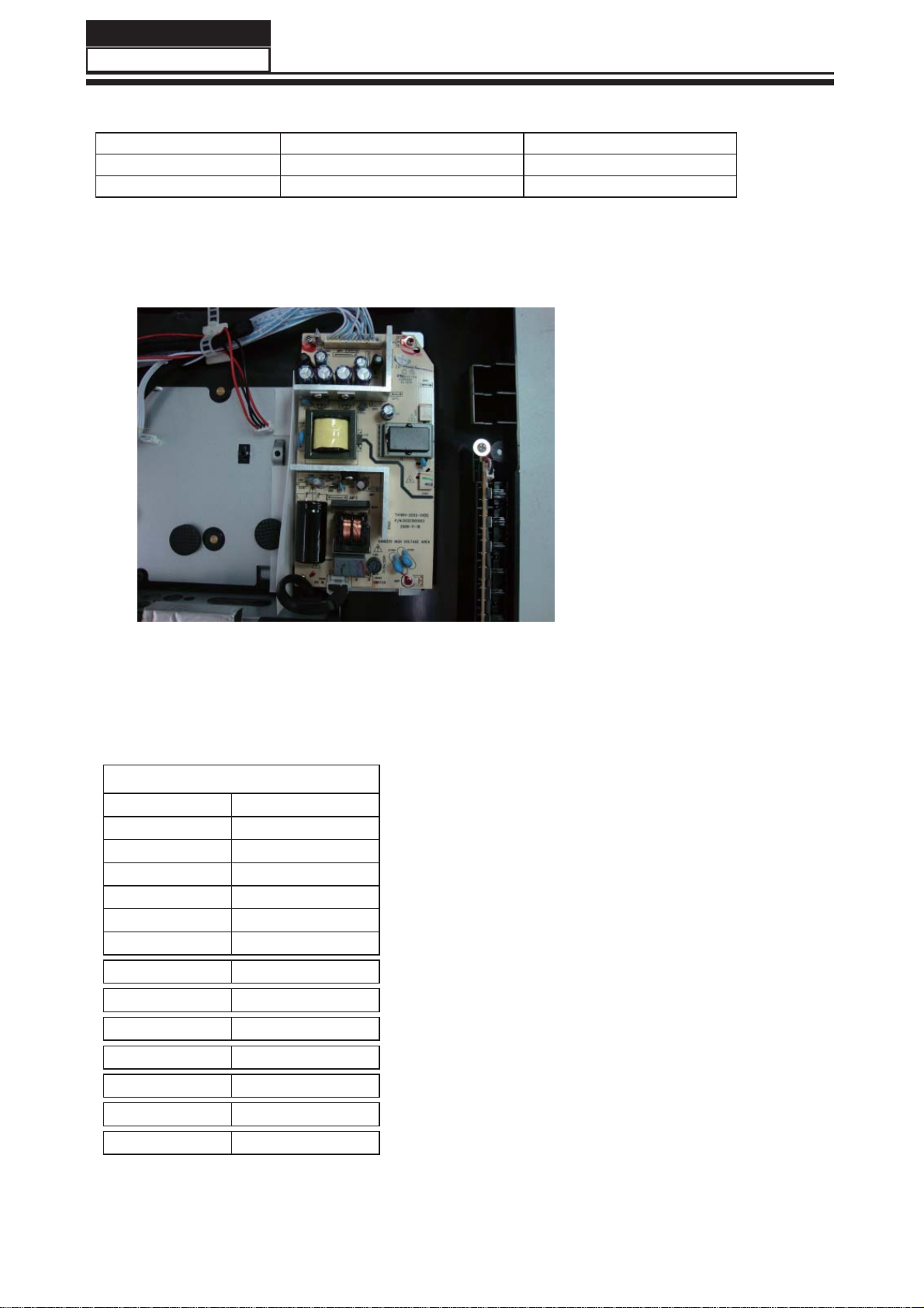
3-3. Power Board
3-3-1 Function Description:
Supply power for Main board, Panel.
3-3-2Connectordefi nition
CON3
Pin number Signal name
1 POWER ON/OFF
2 +12V
3 +12V
4 GND
5 GND
6 +5V
7 +5VSTB
8 +5V
9 GND
10 GND
11 PB
12 BR
13 NC
- 11 -
Page 13
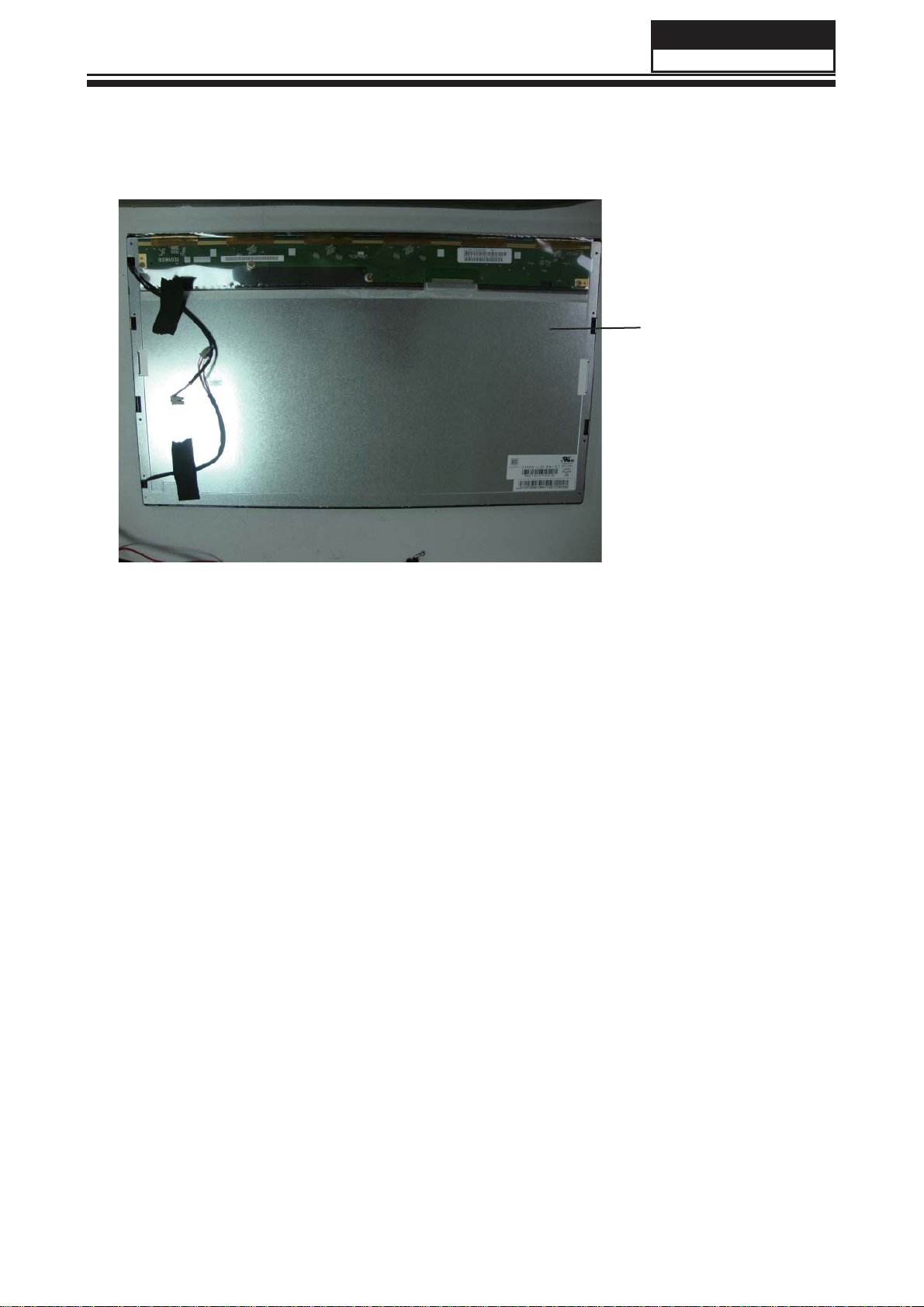
3-4. LCD Panel
Service Manual
Model No.:
V185B1-L06
- 12 -
Page 14
Service Manual
(2)
(2)
(2)
g
g
g
k
(2)
(3)
(2)
Model No.:
3-4-1 Function Description: Display the signal.
3-4-2 Connector defi nition.
CN1
Pin No. Symbol Description Note
1 NC No Connection
2 NC No Connection
3 NC No Connection
4 GND Ground
5RX0- Ne
6 RX0+ Positive transmission data of pixel 0
7 GND Ground
8RX1- Ne
9 RX1+ Positive transmission data of pixel 1
10 GND Ground
11 RX2- Negative transmission data of pixel 2
12 RX2+ Positive transmission data of pixel 2
13 GND Ground
14 RXCLK- Ne
15 RXCLK+ Positive of clock
16 GND Ground
17 RX3- Negative transmission data of pixel 3
18 RX3+ Positive transmission data of pixel 3
19 GND Ground
20 NC No Connection
21 SELLVDS Select LVDS data format
22 NC No Connection
23 GND Ground
24 GND Ground
25 GND Ground
26 VCC Power supply: +5V
27 VCC Power supply: +5V
28 VCC Power supply: +5V
29 VCC Power supply: +5V
30 VCC Power supply: +5V
Note (1) Connector part no.: JAE FI-X30SSL-HF (1.0mm LVDS) or compatible
ative transmission data of pixel 0
ative transmission data of pixel 1
ative of cloc
Note (2) Reserved for CMO internal use, please leave it open
Note (3) Low: JEIDA data format. High/open: VESA data format.
Note (4) Logic level voltage definition: Low: 0V, High: 3.3V
- 13 -
Page 15

CN101 (Header):S14B-PH-SM4-TB (D)(LF)(JST) or equivalent.
Service Manual
Model No.:
- 14 -
Page 16

Service Manual
Model No.:
4. Disassemble and assemble
4-1 Remove the Pedestal 4-3. Remove the adhesive tape
(The location of the adhesive tape as follows)
Lay down the unit so that rear cover
faces upward
Remove the four screw from the
rear cover indicated with ○
Then remove the pedestal
4-2Remove the Back Cover
Remove the adhesive tape indicated on the
fi gure above
Remove the these screw indicated on
fi gure above by ○
Then remove the back cover from the
unit.
- 15 -
Page 17

4-4 Remove the Terminal Bracket
Remove the fi ve screw indicated on the
fi gure above by ○
Then put the terminal bracket to the side
Service Manual
Model No.:
Remove the two screw indicated
on the fi gure above by ○
Disconnected the coupler CON4
CN16CN17
CN6CN5CN4CN8 CN2 CN3
Remove the Main board
4-5 Remove the power module
Remove the six screw indicated on the
fi gure above by ○
Then remove the power module
4-6 Remove the Main board
- 16 -
Page 18

Service Manual
Model No.:
4-7 Remove the speaker
Take out the speaker
4-8 Remove the remote control
Remove the screw, take out the remote control
board
- 17 -
Page 19

5. Installation Instructions
5-1 External Equipment Connections
Accessories
Service Manual
Model No.:
3
2
5 6
ENTER
S.M
P.M
ASPECT
AUTO
SLEEP V-CHIP CC
GOTO MENU SETUP
DISPLAY
MUTE
MTS/SAP
RECALL
SOURCE
TV DISPLAY
SUBTITLE AUDIO
+
CH
_
User GUIDE
Battery
POWER
1
4
7 8 9 0
MENU
EXIT
+
VOL
_
DVD/USB
RETURN
Remote Control
Antenna Connection
Connect one end of a coaxial cable (not included) to the ANT IN jack on the back of
your TV/DVD combo, then connect the other end of the cable into the antenna or cable
TV wall outlet.
To improve picture quality from an antenna in a poor signal area, install a signal
amplifi er.
If you need to split the antenna signal to connect two TVs, install a two-way splitter.
- 18 -
Page 20

Service Manual
Model No.:
This TV provides one AV, and one YPbPr (component) input for convenient
connection to VCR,DVD or
other video equipment. Please refer to the owner s manual of the equipment to
be connected as well.
It can be connected to the following devices: VCR, multi disc player, DVD, camcorder,
video game
or stereo system, etc.....
YPbPr can support these video formats:480i,576i,480p,576p,720p,1080i,1080p,
- 19 -
Page 21

Service Manual
Model No.:
- 20 -
Page 22

Service Manual
Model No.:
5-2 HDMI Connections
When the source device(DVD player or Set Top Box) supports HDM
How To Connect
1. Connect the source device to HDMI port of this TV with an HDMI cable(not supplied
with this product).
2. No separated audio connection is necessary.
How To Use
If the source device supports Auto HDMI function, the output resolution of the source
device will be automatically
set to 1280x720p.
If the source device does not support Auto HDMI, you need to set the output resolution
appropriately.
To get the best picture quality, adjust the output resolution of the source device to
1280x720p.
Select HDMI input source in input source option of Select Main source menu.
When the source device(DVD player or Set Top Box) supports DVI
How To Connect
1. Connect the source device to HDMI port of this TV with a HDMI-to-DVI cable(not
supplied with this product).
2. A separated audio connection is necessary.
3. If the source device has an analog audio output connector, connect the source device
audio output to DVI Audio In port located on the PC port.
How To Use
If the source device supports Auto DVI function, the output resolution of the source device
will be automatically
set to 1280x720p.
If the source device does not support Auto DVI, you need to set the output resolution
appropriately.
To get the best picture quality, adjust the output resolution of the source device to
1280x720p.
Press the INPUT button to select HDMI input source in input source option of Select Main
source menu.
Installation
- 21 -
Page 23

Cable sample
Service Manual
Model No.:
HDMI Cable
(not supplied with the product)
HDMI to DVI Cable
( not supplied with the product)
Analog Audio Cable
(Stereo to RCA type)
(not supplied with the product)
- 22 -
Page 24

Service Manual
Model No.:
Power source
TO USE AC POWER SOURCE
Use the AC polarized line cord provided for operation on AC.
Insert the AC cord plug into a standard polarized AC outlet.
NOTES:
■ Never connect the AC line cord plug to other than the specifi ed voltage.
Use the attached power cord only.
■ If the polarized AC cord does not fi t into a non-polarized AC outlet,
do not attempt to fi le or cut the blade. It is the user`s responsibility to have an
electrician replace the obsolete outlet.
■ If you cause a static discharge when touching the unit and the unit fails to function,
simply unplug the unit from the AC outlet and plug it back in. The unit should return to
normal operation.
- 23 -
Page 25

6. Operation Instructions
Basal information
6-1 Front panel controls
Service Manual
Model No.:
SOURCE
MENU
CH+
CH-
VOL+
VOL-
POWER/STANDBY
1 SOURCE
Display the input source menu.
2 MENU
D isplay the main MENU.
3 CH+/CH-
In TV mode press CH+ or CH- to change
the channel up and down.
In MENU mode, press CH+ or CH- to select
items .
4 VOL+/VOL-
Adjust sound level.
In MENU mode, press VOL+ or VOL- to
adjust the item that you selected.
POWER/STANDBY
5.
Press this button to turn the unit ON from
STANDBY mode.
Press it again to turn the set back to STANDBY mode.
6.2 Back panel controls
RF INPUT
PC
AUDIO INPUT
Y
COMPONENT
Pb
AV
Pr
VGA INPUT
HDMI
R
L
All the terminals are (from left to right):
AC POWER, ANTENNA SOCKET, PC AUDIO input, Audio input, YPbPr (component) input,
AV input, VGA, HDMI input.
Note: 1.AV and YPbPr share the Audio input jacks.
2. When the HDMI port receives a DVI signal, the audio signal used will be from the PC
Audio input jack.
- 24 -
Page 26

Service Manual
Model No.:
6-3 Setting Up Your Remote Control
REMOTE CONTROL
POWER
1
1
2
2
5
4
7 8
MENU
3
ENTER
AUTO
GOTO
DISPLAY
S.M
P.M
AUDIO
+
_
SLEEP V-CHIP CC
10
4
5
EXIT
6
7
8
9
VOL
DVD/USB
RETURN
3
6
9 0
ASPECT
MENU
MUTE
MTS/SAP
RECALL
SOURCE
TV DISPLAY
+
CH
_
SETUP
SUBTITLE
11
12
13
14
15
16
17
18
19
20
21
1: POWER
TV on/off
2: NUMBER KEY:
For direct access to program. For
a 2 (3) digit program number,
The second (third) digit must be
entered before the dash disappears.
The number, the name (and the sound
mode, in analogue mode) are displayed
for a few seconds.
3: MENU
To display TV menu or to return to the
previous menu.
4: CURSOR
To move within the menu.
5: EXIT
To exit menu.
6: VOL+/-
To adjust the sound level.
7: P.M
To switch the picture mode.
8: AUTO
Auto adjust in PC mode.
9: SLEEP
Set the time to turn off the TV.
10:V-CHIP
Set the V-chip level .
11: MUTE
To disable or enable the sound.
12: MTS/SAP
Switch the sound: stereo, SAP or mono.
13: RECALL
To access the previously viewed
program.
14: SOURCE
Change the input source.
15: ENTER
Confirms selection.
16: TV DISPLAY
Displays/hides the program
information
17: S.M
To switch the sound mode.
18: CH+/CH-
To access the next or previous
Program.
19: ASPECT
To change the picture aspect ratio.
20: CC
Switch the closed caption mode (CC1 CC4,Text1-Text4)
21: DVD keys :(optional)
Please refer to the user manual for
DVD player if DVD mode is available.
- 25 -
Page 27

7. Electrical parts
7-1. Block diagram
12V5V5VSB
POWER
EEPROM
LDO&DC-DC
3.3V
1.26V
LED PANEL
Service Manual
Model No.:
BLACKLIGHT
FLASH
REMOTE
CONTROL KEY
HDMI
VGA
INPUT
YPbPr
TSUMV26KU
AV
EARHPONE
OUTPUT
F4558
TPA1517P
VIDEO SAW
SOUND SAW
TUNER
- 26 -
Page 28

Service Manual
Model No.:
7-2. Circuit Diagram
1
2.1mA
VDDP_PM+3.3V_SB
VDDP_PM & AVDD_MPLL must be alive
For PM Mode==>
2
+3.3V_SB
4
3
8.8mA
C1
0.1uFC10.1uF
3.29V 11.3mA
+3.3V_SB
3
IN
IN
2
OUT
OUT
1
ADJ
ADJ
U1
U1
AMS1117-3.3
AMS1117-3.3
R1NCR1
NC
AVDD_MPLL
L1
L1
+5VSB
R40RR4
C7
C6
C5
2.2uFC52.2uF
FB120R/200mA
FB120R/200mA
EC19
EC19
12
+
+
C4
C2
0R
100pFC7100pF
0.1uFC60.1uF
220uF/16V
220uF/16V
0.1uFC40.1uF
0.1uFC20.1uF
C17
0.1uF
C17
0.1uF
C16
0.1uF
C16
0.1uF
C15
0.1uF
C15
0.1uF
C14
0.1uF
C14
0.1uF
C13
0.1uF
C13
0.1uF
C12
0.1uF
C12
0.1uF
VDDP
C11
0.1uF
C11
0.1uF
C10
0.1uF
C10
0.1uF
C9
0.1uFC90.1uF
AVDDA
C8
2.2uFC82.2uF
L2
YPbPr 1080P 416mA
FB42R/4AL2FB42R/4A
+3.3V
AVDD_AU
+3.3V
C24
0.1uF
C24
0.1uF
H2NCH2
H1NCH1
C25
C25
AVDD_VIF
L4
FB120R/1AL4FB120R/1A
TV 141mA
C28
C28
C27
C27
C26
C26
10uF
10uF
0.1uF
0.1uF
0.1uF
0.1uF
100pF
100pF
Date: DEC. 12,2009
APPRD:
1
CHECKED:
0.1uF
0.1uF
0.1uF
0.1uF
0.1uF
0.1uF
SHEET: 1 OF 9 VER:1.0
DESIGN:George Guo
MODEL: MSTV2203-N1
TITLE: POWER
2
3
NC
NC
C37
C37
C36
C36
C35
C35
VDDC
C34
2.2uF
C34
2.2uF
VCC1.26V
4
5
POWER INPUT
510R
1.66A
+5V
123
J1
DVD POWER
+5V
4
EC1
EC1
12
+
+
ކߏ⬉⌕
CON4J1CON4
+5VSB
11.72V 486mA (Audio 100%)
EC2
+12V
EC2
12
+
+
470uF/16V
470uF/16V
1.47A
5.02V 911mA/1.04A (TV/1080P)
ކߏ⬉⌕
MAINPOWER
MAINPOWER
R31KR3
R21KR2
470uF/25V
470uF/25V
R6NCR6
1K
R5
1K
H:ON
L:OFF
POWER-ON/OFF
820R
1
Q1
NC
4.7KR54.7K
3904Q13904
H:ON
L:OFF
PWR_ON/OFF
4.7KR74.7K
R7
1
2 3
Q2
3904Q23904
2 3
+5VSB
5.06V 20.6mA
12
+
+
EC3
EC3
12345678910111213
J2
J2
121mA
Standby Mode:
+5VSB 5.06V 18.9mA
ކߏ⬉⌕
220uF/16V
220uF/16V
+3.3V
FB7
FB42R/4A
FB7
FB42R/4A
EC17
EC17
12
+
+
C22
3.30V
C22
R8NCR8
YPbPr 1080P 442mA
2
VOUT
ADJ
TAB
4
VIN
3
C19
0.1uF
C19
0.1uF
EC20
EC20
12
+
+
FB1 FB42R/4AFB1 FB42R/4A
+5V
220uF/16V
220uF/16V
0.1uF
0.1uF
NC
U2
U2
1
220uF/16V
220uF/16V
AMS1117-3.3
AMS1117-3.3
VCC1.26V
FB6
FB42R/4A
FB6
FB42R/4A
EC18
220uF/16V
EC18
220uF/16V
12
+
+
C32
0.1uF
C32
0.1uF
C30
20PF
C30
L5
22uH_2AL522uH_2A
FB3 FB42R/4AFB3 FB42R/4A
+5V
20PF
R13
12K
R13
12K
U3 PAM2301-ADJ
U3 PAM2301-ADJ
R12
R12
C29
0.1uF
C29
0.1uF
C33
10uF
C33
10uF
FB4NCFB4
+5VSB
R15
100K
R15
100K
100K
5
OUT/FB
GND
PAM2301
PAM2301
EN
1
100K
4
2
C38
C38
100PF
100PF
5
R14
R14
3
LX
VIN
4
100R
100R
NC
1.28V
TV 336mA
R90RR9
0R
D D
C C
B B
A A
- 27 -
Page 29

Service Manual
Model No.:
10K
10K
R34NCR34
NC/10K
NC/10K
Q3
Q3
HOTPLUG
R35 4.7KR35 4.7K
1
32
Q4
HPD
HDMICEC
HDMICECCEC
NC/2N7002
NC/2N7002
HOTPLUG
3904Q43904
NC
R36
NC/10K
R36
NC/10K
Date: DEC. 12,2009
TITLE: HDMI IN
1
APPRD:
CHECKED:
SHEET: 2 OF 9 VER:1.0
2
DESIGN:George Guo
MODEL: MSTV2203-N1
3
4
1
R32
R32
HDMI_5V
24C02=>EDID code must
be upto 256byte space,
for HDMI interface.
2
SDA_HD
10K
10K
10K
10K
SCL_HD
SCL_HD
SDA_HD
R20 100RR20 100R
R21 100RR21 100R
DDC_SCL
DDC_SDA
CEC
HPD
DDC_CLK_IN
DDC_DAT_IN
E4
E3
E2NCE2
E1
HDMI_5V
+5V
D1
3
4
BAV70LD1BAV70L
HD5V
R17
R17
R16
R16
HDMI_5V
V800AAE4V800AA
V800AAE3V800AA
NC
V800AAE1V800AA
B_TX0+
B_TX0-
B_TX0+
B_TX0-
R23 5R1R23 5R1
R22 5R1R22 5R1
RX_0-
RX_0+
G_TX1+
G_TX1-
G_TX1-
G_TX1+
R24 5R1R24 5R1
R25 5R1R25 5R1
RX_1-
RX_1+
R_TX2+
R_TX2-
R_TX2-
R_TX2+
R26 5R1R26 5R1
R27 5R1R27 5R1
RX_2-
RX_2+
TXCLK+
TXCLK-
TXCLK+
TXCLK-
R29 5R1R29 5R1
R28 5R1R28 5R1
RX_C-
RX_C+
E12NCE12
E11NCE11
E10NCE10
E9NCE9
E8NCE8
E7NCE7
E6NCE6
E5NCE5
HOTPLUG
NC
NC
NC
NC
NC
NC
NC
NC
HDMI_5V
+3.3V_SB
+5VSB
R311KR31
R30
R30
1K
23
GND20GND21GND22GND
HDMI
CN1
CN1
5
D D
16
15
18
17
+5V
DDC SCL
DDC SDA
CEC/DDC GND
13
CEC
19
HPD
5
2
8
Dat1 shield
Dat2 shield
Dat0 shield
11
clk shield
7
DAT0+
9
DAT0-
C C
4
DAT1+
6
DAT1-
3
1
DAT2+
10
clk+
DAT2-
12
clk-
HDMI
HDMI
CEC
B B
R33NC/0R R33NC/0R
5
A A
- 28 -
Page 30

Service Manual
Model No.:
1
Date: DEC. 12,2009
BIN+
GIN+
RIN+
C43 47nFC43 47nF
R42 47RR42 47R
C44 47nFC44 47nF
R43 47RR43 47R
C45 1nFC45 1nF
R44 0RR44 0R
SOG
close to MST IC
VGA_HS
R48 100RR48 100R
VGA_VS
R49 100RR49 100R
R51
R51
4.7K
4.7K
TITLE: VGA IN
TXD0
RXD0
2
PC_Lin
PC_Rin
PC_Rin
C40 2.2uFC40 2.2uF
C41 2.2uFC41 2.2uF
R40
12K
R40
12K
R39
12K
R39
3
12K
C42 47nFC42 47nF
R41 47RR41 47R
1
APPRD:
CHECKED:
SHEET: 3 OF 9 VER:1.0
2
DESIGN:George Guo
MODEL: MSTV2203-N1
3
R50
4.7K
R50
VS_RGB
VGA-SDA
4.7K
E19
V800AA
E19
V800AA
E18NCE18
NC
VGA-SCL
E21
E21
V800AA
V800AA
E20
E20
V800AA
V800AA
3
VGA-DDC-5V
D2
1
VGA_5V
RXD0
TXD0
R56 100RR56 100R
R58 100RR58 100R
VGA-SCL
4.7K
4.7K
4.7K
4.7K
VGA-SDA
4
5
R53
R53
R54
R54
BAV70LD2BAV70L
2
+5V
75R
75R
R47
R47
R38
47K
R38
PC-R
PC-R
PC-L
12345
47K
E14NCE14
E13NCE13
NC
NC
VGA-B
VGA-G
VGA_5V
5104938271
CN3
CN3
1514131211
R37
47K
R37
47K
PC-L PC_Lin
4
CN2
PC_AUDIO_IN
CN2
PC_AUDIO_IN
5
VGA-R
6
E17NCE17
E16NCE16
E15NCE15
R46
R46
R45
R45
VGA
VGA
17
16
75R
75R
75R
75R
NC
NC
NC
HS_RGB
D D
C C
B B
A A
- 29 -
Page 31

Service Manual
Model No.:
REAR_A-Lin
REAR_A-Lin
1
2
3
4
5
C48 2.2uFC48 2.2uF
R64 22KR64 22K
HD_Yin
C47 2.2uFC47 2.2uF
HD_Y REAR_AUDIO_L
REAR_AUDIO_L
11229933884
CN4
CN4
+5V_LDO
DVD-Lin
DVD-Rin
R63 100RR63 100R
R62 100RR62 100R
DVD_AR
DVD_AL
1234567
DVD
R70
R70
E22NCE22
NC
REAR_AUDIO_R
L
L
Y
Y
R75
R75
R57
R57
R59
R59
R303
100K
R303
100K
R301
100K
R301
100K
R302
100K
R302
100K
R68
R68
R60
R60
DVD_AV
R66 47RR66 47R
R67
R67
DVD_CVBS
J3
7pin 2.0mmJ37pin 2.0mm
12K
12K
100K
100K
100K
100K
100K
100K
12K
12K
12K
12K
SC_Yin
SC_Pbin
HD_Yin
HD_Pbin
+3.3V_SB
75R
75R
SC_Prin
HD_Prin
REAR_A-Rin
REAR_A-RinREAR_AUDIO_R
C50 2.2uFC50 2.2uF
R77
R77
R72 22KR72 22K
E23NCE23
HD_Pbin
C49 2.2uFC49 2.2uF
HD_Pb HD_Pb
HD_Y
4
R55
R55
R19
R19
R52
R52
R248
R248
R238
R238
R247
R247
DVD_ON/OFF
DVD_ON/OFF
R71NCR71
NC
R74
150R
R74
150R
12K
12K
NC
R
R
Pb
Pb
100K
100K
100K
100K
100K
100K
100K
100K
100K
100K
100K
100K
+8V
IR_in
IR_in
R78
100R
R78
100R
HD_PrinHD_Pr
C51 2.2uFC51 2.2uF
HD_Pr
R79
R79
SCART Input
REAR_AV
R8375R R8375R
R8275R R8275R
R8175R R8175R
R87 47RR87 47R
E26
E26
V800AA
V800AA
E25
E25
V800AA
V800AA
E24
E24
REAR_CVBS
V800AA
V800AA
REAR_CVBS
6
55776
V
V
Pr
Pr
AUOutL2
C55
2.2uF
C55
2.2uF
R86
4.7k
R86
4.7k
47k
47k
R85
R85
1
4.7k
4.7k
2 3
Q5
3904Q53904
R80
100R
R80
100R
Scart1_L
C53
2.2uF
C53
2.2uF
R84
10K
R84
10K
E27
E27
V800AA
V800AA
Scart1_Lout
SC_Yin
SC_Prin
SC_Pbin
C56 2.2uFC56 2.2uF
C52 2.2uFC52 2.2uF
C54 2.2uFC54 2.2uF
SCART_R
SCART_B
SCART_G
CVBSIN1GND2CVBSOUT3GND4FC_FSW5GND6R7GND8G9GND10SC_FS11B12GND13LIN14LOUT15RIN16ROUT
J4
LinkJ4Link
SC_FB_IN
SCART1_VOUT
SC_CVBS
SCART_R
R93
75R
R93
75R
E31NCE31
AV-JACK-1
AV-JACK-1
10K
10K
R92
R92
47R
47R
R91
R91
Location
Near RCA.
R9075R R9075R
R8975R R8975R
R8875R R8875R
E30
E30
E29
E29
E28
E28
SC_FS_IN
SCART_B
SCART_G
PH_R
NC
V800AA
V800AA
V800AA
V800AA
V800AA
V800AA
AV1-L
Scart1_Lout
PH_L
AV1-R
Scart1_Rout
PH_DETECT
PH_DETECT
47R
47R
R94
R94
17
+8V
SCART_AV
SC_CVBS
SIDE-Rin
R95 22KR95 22K
E33NCE33
+8V
R98
R98
RN5
100KX4
RN5
100KX4
R96
75R
R96
75R
E32NCE32
NC
Blanking I/O
12K
12K
R97
R97
R100
R100
C57
C57
SC_FB_IN SC_FB
4.7k
4.7k
100R
100R
2.2uF
2.2uF
NC
RN4
RN4
7531
7531
7531
7531
7531
7531
RN3
RN3
R103
R103
Scart1_R
Scart1_Rout
SCART-Lin
AV1-L
R99
75R
R99
75R
E34
E34
V800AA
V800AA
E36NCE36
J5
100KX4
100KX4
100KX4
100KX4
C58
C58
R321
R321
R102
R102
E35
E35
SIDE-Lin
R108
12K
R108
12K
R104 22KR104 22K
NC
123456789
MUX_Rin
MUX_Lin
C166 2.2uFC166 2.2uF
C165 2.2uFC165 2.2uF
3
X13Y
U6
X012X114X215X311Y01Y15Y22Y34A10B
8642
8642
8642
8642
8642
8642
C60 2.2uFC60 2.2uF
C59 2.2uFC59 2.2uF
C61 2.2uFC61 2.2uF
SCART-Lin
SIDE-Lin
DVD-Lin
AUOutR2
2.2uF
2.2uF
4.7k
4.7k
R110
R110
47k
47k
1
R109
R109
2 3
Q6
3904Q63904
10K
10K
V800AA
V800AA
R106
12K
R106
12K
R101
22K
R101
22K
E37NCE37
NC
SC_FS
SC_FS
R105
R105
SC_FS_IN
Switch
SIDE_AV
R112 47RR112 47R
SIDE_CVBS
+8V
16
C62 2.2uFC62 2.2uF
DVD-Rin
10K
10K
47R
47R
SCART-Rin
AV1-R
R107
2.7K
R107
2.7K
15K
15K
Date: DEC. 12,2009
APPRD:
CHECKED:
SHEET: 4 OF 9 VER:1.0
DESIGN:George Guo
MODEL: MSTV2203-N1
TITLE: VIDEO IN&OUT
SCART RGB/FS
1
Q11
Q11
2 3
4.7K
4.7K
HD_AUD_SW0
EC4
ৠℹ᳝༅ⳳˈⷁ
AV
1
2
3
4
5
R115
75R
R115
75R
E40NCE40
NC
101112
13
13pin 1.25mmJ513pin 1.25mm
C65
0.1uF
C65
0.1uF
6
8
7
INH
VEE
VCC
GND
AU_SW0
R116 10KR116 10K
C63 2.2uFC63 2.2uF
C64 2.2uFC64 2.2uF
SCART-Rin
SIDE-Rin
R114
12K
R114
12K
R111
22K
R111
22K
E39NCE39
NC
2K
R1130RR113
0R
E38NCE38
NC
SIDE-AV
SCART
0 DVD
74HC4052U674HC4052
PIN9 PIN10
0
11
10
01
AU_SW1 AU_SW0 INput
9
Q8
3904Q83904
2 3
R119
4.7K
R119
4.7K
1
AU_SW1
Q7
3904Q73904
2 3
R118
4.7K
R118
4.7K
1
R117 10KR117 10K
+8V
560R
HD_AUD_SW0
HD_AUD_SW1
MUX1_YIN
MUX1_PBIN
MUX1_PRIN
MUX_VS
HD_Pbin
HD_Prin
HD_Yin
VGA_VS
MUX_VS
MUX1_YIN
MUX1_PBIN
MUX1_PRIN
R11 NC/33RR11 NC/33R
R10 NC/33RR10 NC/33R
R18 NC/33RR18 NC/33R
R320 NC/33RR320 NC/33R
C170 2.2uFC170 2.2uF
C172 2.2uFC172 2.2uF
C171 2.2uFC171 2.2uF
C69
0.1uF
C69
0.1uF
C66
2.2uF
C66
2.2uF
12
7
16
15
8
DA4DB
EN
DC9DD
VCC
L6
FB120R/200mAL6FB120R/200mA
U7
+5V_LDO
YPbPr/SCART Input 2:1 Switch
+5V_LDO
S1A2S1B5S1C11S1D14S2A3S2B6S2C10S2D13IN
PI5V330U7PI5V330
HD_Pbin
HD_Prin
SC_Yin
HD_Yin
VGA_VS
VGA_VS
CVBS_OUT
CVBS_OUT
C68
10uF
C68
10uF
R121
22K
R121
22K
1
R120
220R
R120
220R
Q10
3904
Q10
3904
1
3 2
Q9
3906Q93906
0.1uF
0.1uF
C67
C67
SC_Pbin
SC_Prin
SC_FB
2 3
+
+
75R
75R
R122
R122
SCART1_VOUT
GND
SC/HD_SW
R125
R125
R124
R124
R123
220R
R123
220R
EC4
EC4
220uF/16V
220uF/16V
E41
E41
YPbPr/VS
1
0
SC/HD_SW
3904
3904
1
R127
R127
R126 1KR126 1K
+3.3V
10K
10K
75R
75R
V800AA
V800AA
D D
C C
B B
A A
- 30 -
Page 32

Service Manual
Model No.:
1
Date: DEC. 12,2009
APPRD:
1
SIF_CTL
SIF_CTL HI B/G,DK,I,L
SIF_CTL LOW L'
NC/4.7K
NC/4.7K
NC/4.7K
NC/4.7K
R129
R129
11
10
9
8
7
6
5
4
3
2
1
11
10
9
8
7
6
5
4
3
2
1
D3NCD3
NC
L7
NC/1uHL7NC/1uH
NC/680R
NC/680R
NC/4.7K
NC/4.7K
NC/15nF
NC/15nF
NC/10uF
NC/10uF
IF_TV
IF_TV
R134
R134
C72
C72
3
AGND
TV_SDA
TV_SCL
SIF_CTL
1
1
0R/NC
0R/NC
0R/NC
0R/NC
IF_TV
5V-Tuner
5V-Tuner
R137
R137
Q13
Q13
2 3
2
Q12
Q12
TV_SDA
TV_SCL
RF-AGC
I2C_SDA
I2C_SDA
R136 100RR136 100R
R132
R132
R131
NC/4.7K
R131
NC/4.7K
2
3
4
TUNER2
TUNER2
5
TUNER1
TUNER1
+5V_LDO
R128
R128
+8V
13
GND15GND12GND14GND
AFT7W103G
AFT7W103G
NC/AFT7W103G
NC/AFT7W103G
13
GND15GND12GND14GND
F21WT-3DAR-E
F21WT-3DAR-E
F21WT-3DAR-E
F21WT-3DAR-E
1K
NC/100R
NC/100R
IFOUT
NC
NC
NC
5VB
NC
SDA
SCL
AS
NC
AGC
IFOUT
NC
33V
NC
5VB
NC
SDA
SCL
AS
NC
AGC
R130
R130
R133
R133
C71
C71
C70
C70
NC/4.7K
NC/4.7K
NC/3904
NC/3904
R142
R142
R141
R141
NC/2SC2216
NC/2SC2216
R140
R140
R135
0R/56R
R135
0R/56R
C73
10nF/15nF
C73
10nF/15nF
R139
NC/75R
R139
NC/75R
I2C_SCL
I2C_SCL
R138 100RR138 100R
C75
C75
C74
C74
SIFP
SIFP
51
SAW
SAW
U8 D9352H/D9650N
U8 D9352H/D9650N
D40RD4
0R
0R/39R
0R/39R
C76
10nF/15nF
C76
10nF/15nF
NC/22R
NC/22R
NC/1.5K
NC/1.5K
TAGC
TAGC
R143 12KR143 12K
22pF
22pF
22pF
22pF
RF-AGC
2
D5 1N4148D5 1N4148
C77
C77
SIFM
SIFM
4
3
R145
R145
D6
NC/BA892D6NC/BA892
R144
R144
+5V_LDO
EC5
EC5
NC/47uF/16V
NC/47uF/16V
0.1uF
0.1uF
0R/NC
0R/NC
NC/4.7K
NC/4.7K
R146
R146
FOR SECAM
VIFP
VIFP
NC
C78NCC78
U9 D7262H/D3953N
U9 D7262H/D3953N
10nF/15nF
10nF/15nF
C79
C79
22K
22K
R148
22K
R148
22K
R147
4.7K/NC
R147
4.7K/NC
5
OUT2
IN
1
SAW
SAW
L8NCL8
D7
+5V
+5V_LDO
+8V
VIFM
VIFM
NC
4
OUT1
GND
3
ING
2
BA892D7BA892
R152
R152
Q14
Q14
3
R151
R151
SIF_CTL
5V-Tuner
5.01V 119mA
FB5
FB5
FB8
NC/FB56R/1A
FB8
NC/FB56R/1A
4
4
+12V
NC
C80NCC80
NC/0R
NC/0R
3904/NC
3904/NC
2
1
4.7K/NC
4.7K/NC
NC/FB56R/1A
NC/FB56R/1A
2
VOUT
TAB
VIN
3
2
VOUT
TAB
VIN
3
L15
L15
R154
R154
C82
C82
R153
R153
10UH
10UH
510R
510R
U11
AMS1084CD-ADJ
U11
AMS1084CD-ADJ
ADJ
1
10uF
10uF
470R
470R
ADJ
1
U10
AMS1084CD-ADJ
U10
AMS1084CD-ADJ
C3
NC/0.1uFC3NC/0.1uF
EC6
470uF/16V
EC6
470uF/16V
+
+
EC16
470uF/16V
EC16
470uF/16V
+
+
R1550RR155
0R
R156
R156
C83
C83
2.49K/%1
2.49K/%1
0.1uF
0.1uF
C84
C84
1.5K
1.5K
R157
R157
0.1uF
0.1uF
CHECKED:
SHEET: 5 OF 9 VER:1.0
2
DESIGN:George Guo
MODEL: MSTV2203-N1
TITLE: TUNER
3
4
5
D D
C C
B B
A A
- 31 -
Page 33

1
2
3
4
5
+5VSB
R159 100RR159 100R
C86
C86
R164
R164
6
J6
J6
6p,2.0,FrontPanel
6p,2.0,FrontPanel
KEY PAD
R160 200RR160 200R
CL=20pf of XTAL
C85
C85
27pF
27pF
C87
10uF
C87
10uF
BAV99D8BAV99
D8
321
+3.3V_SB
R158
R158
Service Manual
Model No.:
Date: DEC. 12,2009
24C32
24C32
C121
C121
NC/22pF
NC/22pF
CZSPI_CZ
SI
SO
8642
8642
7531
7531
SPI_DI
SPI_DO1
APPRD:
1
CHECKED:
SHEET: 6 OF 9 VER:1.0
DESIGN:George Guo
MODEL: MSTV2203-N1
TITLE: TSUMV26KU
2
3
4
RN11 22RX4
RN11 22RX4
5
IR_in
22pF
22pF
IR_in
C89
C89
10uF
10uF
R165 0RR165 0R
KEY0-SAR0
0R
R1670RR167
4.7K
4.7K
LED_G
LED_R
KEY_STB
11223344556
AVDD_VIF
AVDD_AU
AVDDA VDDPVDDC
AVDD_MPLL
VDDP_PM
HWRESET
R1621MR162
1M
X1
14.318MHZX114.318MHZ
C88
C88
27pF
27pF
C91
1nF
C91
1nF
HWRESET
R166
R166
100R
100R
SYS_RST
Q15
3906
Q15
3906
R168
22K
R168
22K
3 2
1
R163 4.7KR163 4.7K
C90
4.7uF
C90
4.7uF
C177
10uF
C177
10uF
100K
100K
D D
+3.3V_SB
27
28
36
38
56
57
64
90
102
116
54
78
118
7
15
123
23
110
113
24
XIN
25
ˈ䰆ℶԡϡ㡃
C177
乘⬭
123
J7
3p,2.0,KeypadJ73p,2.0,Keypad
V800AA
V800AA
E43
E43
E42
E42
V800AA
V800AA
R173 0RR173 0R
R170 0RR170 0R
R169
5.1K
R169
5.1K
C93
470pF
C93
470pF
R172
5.1K
R172
5.1K
C92
C92
470pF
470pF
KEY1-SAR1
KEY0-SAR0
PANEL
INTERFACE
RXO3+
RXO3-
RXOC+
RXOC-
RXO2-
RXO2+
RXO1-
RXO0+
RXO1+
RXO0-
RXE0-
RXE0+
RXE1-
RXO1+
RXO0-
RXOC+
RXO2-
RXOC-
RXO3+
RXO2+
RXO3-
RXO0+
RXO1-
RXE0+
RXE0-
8642
8642
8642
8642
8642
8642
7531
7531
7531
7531
7531
7531
RN9 22RX4
RN9 22RX4
RN8 22RX4
RN8 22RX4
RN7 22RX4
RN7 22RX4
RN6 22RX4
RN6 22RX4
91
95
97
99
100
LVA0P
AVDD_VIF
AVDD_VIF
AVDD_VIF
AVDD_AU
VDDP
VDDP
VDDP
VDDP
VDDP
VDDP
VDDC
VDDC
VDDC
AVDD_ADC
AVDD_ADC
AVDD_DVI
AVDD_MPLL
VDDP_2
HWRESET
XOUT
RXACKN
DDCDB_DA
DDCDB_CK
120
119
112
111
SDA_HD
SCL_HD
TXCLK-
TXCLK+
B_TX0-
B_TX0+
TXCLK+
TXCLK-
B_TX0-
TXCLK-
TXCLK+
98
LVA1P
LVA0M
RXACKP
RXA0N
121
B_TX0-
G_TX1-
B_TX0+
G_TX1-
LVA1M
RXA0P
122
B_TX0+
G_TX1+
G_TX1+
96
124
G_TX1-
R_TX2-
LVA2P
RXA1N
R_TX2-
125
G_TX1+
R_TX2+
94
LVA2M
LVACKP
RXA1P
HPLUGA
126
HOTPLUG
SDA_HD
R_TX2+
SDA_HD
93
127
R_TX2-
SCL_HD
SCL_HD
92
LVA3P
LVACKM
RXA2P
RXA2N
128
R_TX2+
HDMICEC
HDMICEC
INPUT
DVI/HDMI
LVA3M
HOTPLUG
HOTPLUG
88
89
LVB0P
PB+
C94 47nFC94 47nF
R171 33RR171 33R
MUX2_PBIN
87
LVB0M
SOY
C95 1nFC95 1nF
R174 0RR174 0R
VGA_HS
LED_G
R1792KR179
2K
+5VSB
R181 4.7KR181 4.7K
+5VSB
RXEC-
RXEC+
RXE3-
RXE3+
RXE1-
RXE2+
RXE2-
RXE1+
RXE1+
RXE2+
RXE2-
RXE3+
RXEC+
RXE3-
RXEC-
8642
8642
8642
8642
7531
7531
7531
7531
RN10 22RX4
RN10 22RX4
80
84
86
83
82
81
85
LVB3P
LVB2P
LVB1P
LVB3M
LVB2M
LVB1M
LVBCKP
LVBCKM
U12
GIN1M5BIN12SOGIN13GIN14RIN16BIN09GIN0M10HSYNC08VSYNC014CVBS2P17CVBS1P18CVBS0P
GIN011SOGIN012CVBSOUT
RIN0
13
16
VGA_HS
MUX_VS
RIN+
SOG
GIN+
BIN+Y+PR+
C97 47nFC97 47nF
C98 47nFC98 47nF
C99 47nFC99 47nF
R177 33RR177 33R
MUX2_PRIN
RIN+
GIN+
SOG
SOG
GIN+
INPUT
VGA
C100 47nFC100 47nF
DVD_AV
R178 68RR178 68R
MUX2_PBIN
MUX2_YIN
MUX2_PRIN
RIN+
MUX2_PBIN
MUX2_YIN
MUX2_PRIN
INPUT
Y,Pb,Pr
C C
C96 47nFC96 47nF
R175 33RR175 33R
MUX2_YIN
MUX_VS
MUX_VS
VGA_HS
R176 68RR176 68R
BIN+
BIN+
Q16
3904
Q16
3904
LED_R
Q17
3904
Q17
3904
R180 2KR180 2K
4.7K
4.7K
R183
R183
LED_CTL
do not use GPIO function in PAD_INT
if the system need HDMI_CEC function
SC_FS
UART-RX
UART-TX
KEY0-SAR0
KEY1-SAR1
IR_in
R186 0RR186 0R
R187 100RR187 100R
R185 0RR185 0R
R182 0RR182 0R
HDMICEC
PWR_ON/OFF
SAR2
108
109
107
114
105
115
106
104
103
INT
IRIN
CEC
SAR1
SAR0
SAR2
WAKEUP
DDCA_DA
DDCA_CK
TSUMV26KU
VIFP
VCOM0
CVBS3P
19
30
21
20
CVBS_OUT
C105 0.1uFC105 0.1uF
C103 47nFC103 47nF
C104 47nFC104 47nF
C101 47nFC101 47nF
C102 47nFC102 47nF
VIFP
SCART_AV
SIDE_AV
REAR_AV
R184 68RR184 68R
Please close
WARNING !!!
DEBUG PORT
LED_CTL
DVD_ON/OFF
R190 100RR190 100R
R191 100RR191 100R
SPI_CK
77
75
SCK
GPIOD[1]76GPIOD[0]
TAGC
VR27
VIFM
SIFM32SIFP
37
35
31
33
C106 0.1uFC106 0.1uF
C107 0.1uFC107 0.1uF
C108 0.1uFC108 0.1uF
VIFM
SIFM
SIFP
TAGC
C81 10uFC81 10uF
C109 0.1uFC109 0.1uF
to chip.
L9
FB120R/1AL9FB120R/1A
+5V
SIDE_AV
REAR_AV
SIDE_AV
REAR_AV
+5VSB
SPI_DI
SPI_CZ
SPI_DO1
73
72
74
SDI
SCZ
SDO
LINE_IN_2L39LINE_IN_2R40LINE_IN_3L41LINE_IN_3R
PC_Lin
C112
C112
C111
C111
R192
4.7K
R192
4.7K
C110
C110
DVD_AV
SCART_AV
SCART_AV
DVD_AV
AMP-MUTE
SIF-CTL
71
AD[0]
AD[1]70AD[2]
MUX_Lin
PC_Rin
100pF
100pF
0.1uF
0.1uF
0.1uF
0.1uF
CVBS_OUT
CVBS_OUT
INPUT
VIDEO
R194
R194
R196
R196
I2C_SCL
R193 100RR193 100R
42
REAR_A-Lin
MUX_Rin
4.7K
4.7K
4.7K
4.7K
I2C_SCL
I2C_SDA
I2C_SDA
R195 100RR195 100R
68
69
AD[3]
LINE_IN_4R44LINE_IN_4L
43
REAR_A-Rin
ON-PBACK
ON-PANEL
67
66
RDZ
WRZ
AUCOM
45
C113 0.1uFC113 0.1uF
R197 0RR197 0R
PC_Lin
PC_Lin
UART-RX
UART-TX
R198 100RR198 100R
R199 100RR199 100R
TXD0
RXD0
PWM freq :
from 6MHz ~ 12M/2^34(=0.0007)Hz
R200 NC/10KR200 NC/10K
PWM0
PWM1
WP_EE
PWM2
PWM3
65
61
60
59
ALE
PWM062PWM1
PWM2
PWM3
AUVRM46AUVRP47AUVREF
LINE_OUT_0L52LINE_OUT_0R
DAC_OUT_0L50DAC_OUT_0R
48
53
51
AUVRADP
AUVRADN
AUVREF
C117
1uF
C117
1uF
C116
4.7uF
C116
4.7uF
C115
0.1uF
C115
0.1uF
C114
10uF
C114
10uF
MUX_Lin
REAR_A-Rin
PC_Rin
REAR_A-Lin
MUX_Rin
MUX_Lin
PC_Rin
MUX_Rin
REAR_A-LIN
REAR_A-Rin
INPUT
AUDIO
RN20
RN20
B B
GND
GND
GND
GND
GND
GND
GND
GND
GND
GND
GND
GND
100RX4
100RX4
AUOutL1_amp
AUOutR1_amp
AUOutL1_amp
117
101
79
63
58
55
49
34
29
26
22
1
8642
8642
7531
7531
AUOutR2
AUOutL2
AUOutL2
AUOutR1_amp
+3.3V_SB
+3.3V
GPIO Control Pins
L10
L10
FB120R/200mA
FB120R/200mA
R65
22K
R65
22K
C174
10nF
C174
10nF
R61
22K
R61
22K
C175
10nF
C175
10nF
R69
22K
R69
22K
C173
10nF
C173
10nF
R73
22K
R73
22K
C176
10nF
C176
10nF
AUOutR2
OUTPUT
AUDIO
DVD_ON/OFF
HD_AUD_SW1
ON_PANEL
AMP-MUTE
ON_PBACK
SIF_CTL
PWR_ON/OFF
HD_AUD_SW0
SIF_CTLSIF-CTL
ON_PANEL
ON_PBACK
HD_AUD_SW0PWM1
R209
10K
R209
10K
10K
10K
R208
R208
R207
10K
R207
10K
R206
10K
R206
10K
R205
4.7K
R205
4.7K
R204
10K
R204
10K
R203
10K
R203
10K
R201
10K
R201
10K
R213 0RR213 0R
R211 0RR211 0R
R210 0RR210 0R
R212 0RR212 0R
R214 0RR214 0R
ON-PANEL
ON-PBACK
DVD_ON/OFF
AMP-MUTE
LED_CTL
PWR_ON/OFF
PWM3 HD_AUD_SW1
R221
4.7K
R221
4.7K
R220
4.7K
R220
4.7K
R219
4.7K
R219
4.7K
I2C_SCL
I2C_SDA
WP_EE
C119
0.1uF
C119
0.1uF
R222 100RR222 100R
+5V +5V
7
8
5
6
WP
SCL
SDA
VCC
I2C address
at A0.
A01A12A23GND
U14
U14
4
+3.3V
R318 51RR318 51R
C118
0.1uF
C118
0.1uF
R319 51RR319 51R
SI
SCK
5
8
7
U13
U13
MX25L4005A
MX25L4005A
FLASH:512KB
CZ
R215
NC/4.7K
R215
NC/4.7K
+3.3V
Mode
Selection
+3.3V
6
SCK
VDD
HOLD#
CE#1SO2WP#3VSS
SO
R218 33KR218 33K
PWM2
1K
R2171KR217
1K
R2161KR216
A A
SI
R298 22RR298 22R
SPI_CK SCK
4
C120
0.1uF
C120
0.1uF
NC
R224NCR224
PWM1PWM1PWM0
ADJ_PWM0
NC
R223NCR223
8
5
7
6
SI
SCK
VDD
HOLD#
CE#1SO2WP#3VSS
FLTPFLTP
4
SIFP
SIFM
TAGC
VIFM
VIFP
TAGC
SIFP
SIFM
VIFM
VIFP
INPUT
VIF
- 32 -
Page 34

Service Manual
Model No.:
+12V
PWD_MT
Q26
Q26
Q25
Q25
R273
R273
PH_DETECT
R274
NC/100K
R274
NC/100K
NC/5V1
NC/5V1
D11
D11
NC/47K
NC/47K
R279
R279
R277
NC/4.7K
R277
NC/4.7K
1
NC/3904
NC/3904
2 3
0R
R2990RR299
3904
3904
10K
10K
MUTE ON
MUTE OFF
AMP-MUTE2
1
Q24
3904
Q24
3904
23
AL+
1N4148
1N4148
Q23
3904
Q23
3904
2 3
1
1K
R2721KR272
D13
0R_1206
D13
0R_1206
PWD_MT
21
HVSSR
HVSSR
C149
0.1uF
C149
0.1uF
20
OUTPR
19
HVDDR
18
OUTPR
17
HVDDR
C152
C152
16
HVDDR
15
OUTNR
EC15
EC15
14
AUDIO_PWR
HVDDR
13
OUTNR
12
HVSSR
11
C150
0.1uF
C150
HVSSR10AVSS2
0.1uF
AMP-ENG-CTL
NC
R276NCR276
C151NCC151
NC
100R
100R
R275
R275
3904
3904
Q27
Q27
2 3
1
1K
R2781KR278
PWD_MT
SPEAKER
SPEAKER
J11
J11
432
1
NC/0R
NC/0R
R250
EC10
EC10
NC/470uF/16V
NC/470uF/16V
R323 NC/0RR323 NC/0R
LOUT-
LOUT+LOUT#
1 2
NC/TPA1517
NC/TPA1517
U16
U16
C134
C134
R250
NC/0R
NC/0R
R249
R249
ROUT-
ROUT+
NC/220nF
NC/220nF
C137
C137
NC/220nF
NC/220nF
C136
C136
+
+
+
+
EC11
NC/470uF/16V
EC11
NC/470uF/16V
1 2
R252
R252
R251
R251
ROUT#
20
IN11SGND2SVRR3OUT14PGND5OUT26VCC7M/SB8IN29GND/HS
NC/2.2uF
NC/2.2uF
AL+
SVRR
LOUT#
R300
R300
MUTE
SVRR ROUT#
NC/2K
NC/2K
NC/2K
NC/2K
AR+
NC/47K
NC/47K
10
12
+
+
GND/HS11GND/HS12GND/HS13GND/HS14GND/HS15GND/HS16GND/HS17GND/HS18GND/HS19GND/HS
C138
C138
EC12
EC12
R254
R254
R253
R253
NC/2.2uF
NC/2.2uF
EC21
EC21
12
+
+
C135
C135
NC/220uF/25V
NC/220uF/25V
NC/2R2
NC/2R2
NC/2R2
NC/2R2
NC/4.7uF/25V
NC/4.7uF/25V
NC/0.1uF
NC/0.1uF
MUTEDD
1
E44
E44
V800AA
V800AA
R2321KR232
1K
Q19
3904
Q19
3904
2 3
R229
22R
R229
22R
+
EC9
220uF/16V+EC9
220uF/16V
AMP_RINPH_LAMP_LIN PH_R
2
R228
R228
EC8
PH_L PH_R
22R
22R
220uF/16V+EC8
220uF/16V
+
E45
E45
1
R240
4.7K
R240
V800AA
V800AA
FOR S2
FOR S2
PWD_MT
Q18
Q18
PWD_MT
4.7K
AUDIO_PWR
R322 3R/3WR322 3R/3W
+12V
3904
3904
2 3
1
R239
4.7K
R239
4.7K
11.86V
470pF
470pF
C126
C126
R2301KR230
1K
470pF
470pF
C124
C124
+5VSB
R255NC R255NC
Mute-VCC
+12V
R2560R R2560R
R261
10K
R261
10K
R260
R260
D10
D10
D9
1N4148D91N4148
1N4148
1N4148
+5VSB
R257 1KR257 1K
R259
10K
R259
10K
G-CTL
R258
NC/10K
R258
NC/10K
gain0LOUT-
470R
470R
R268
R268
+3.3V_SB
gain1
12
R265
R265
R264
R264
EC14
EC14
NC/10K
NC/10K
10K
10K
1
220uF/25V
220uF/25V
R267
NC/10K
R267
NC/10K
R266
R266
MUTEDD
R316
R316
NC/3K
NC/3K
Q22
3904
Q22
3904
R317 0RR317 0R
Q20
3906
Q20
3906
R271 10KR271 10K
3 2
270K
270K
10K
10K
MUTE
D12
D12
PH_Drive
3
R262
10K
R262
10K
+12V
LOW:shut down
HIGH:OPERATING
U17
U17
31
32
33
34
35
36
37
38
39
40
41
LOUT+
30
29
FBPL
HVSSL
HVSSL
OUTPL
HVDDL
OUTPL
HVDDL
HVDDL
MSH9000 (QFN40 IC)
MSH9000 (QFN40 IC)
OUTNL
HVDDL
OUTNL
HVSSL
thermal
HVSSL1G1
2
gain1
28
FBNL
VIPL3VINL
C144 0.47uFC144 0.47uF
AL+
+5VSB
C145 0.47uFC145 0.47uF
AL-
27
NC
4
AMP-EN
26
gain0
HIGH:MUTE
R2631KR263
C146 1uFC146 1uF
24
25
EN
AVDD
AVSS1
MUTE
7G05
6
C147 0.47uFC147 0.47uF
MUTE_msh9000
AR-
R269 10KR269 10K
LOW:OPERATING
1K
MUTE_msh9000
23
C148 0.47uFC148 0.47uF
AR+ ROUT-
ROUT+
22
FBPR
FBNR
VIPR8VINR
9
Q21
3904
Q21
3904
2 3
1
R270 1KR270 1K
MUTE
LOUT-
LOUT+
220nF
220nF
C140
C140
C143
0.1uF
C143
0.1uF
L12
L12
18uH/3A
18uH/3A
R235
R235
22K
22K
AL+
10nF
10nF
C128
C128
4
+8V
5
R233 1KR233 1K
R234 NCR234 NC
C127 2.2uFC127 2.2uF
C123
10uF+C123
10uF
VCC-OP2
AMP_LIN
+
1
U15A
4558
U15A
4558
84
-
+
-
+
3
2
R231
10K
R231
10K
C125
2.2uF
C125
2.2uF
AUOutL1_amp
R237 33KR237 33K
4VA
ᯊˈⷁ
4558
ϡ⫼
R225
10K
R225
10K
R227
47K
R227
47K
R226
10K
R226
10K
4VA
+
+
C122
C122
10uF
10uF
VCC-OP2
R241
R241
AR+
R243 1KR243 1K
C131 2.2uFC131 2.2uF
AMP_RIN
7
U15B 4558
U15B 4558
84
+
+
5
47K
47K
10nF
10nF
C132
C132
-
-
6
R242
R242
C130
C130
AUOutR1_amp
R244
R244
22K
22K
R245 NCR245 NC
R246 33KR246 33K
10K
10K
ᯊˈⷁ
4558
2.2uF
2.2uF
ϡ⫼
+12V
L11
18uH/3A
L11
18uH/3A
Mstar Audio Amp + 8 Speaker
C139
C139
EC13
EC13
470uF/25V
470uF/25V
C141
0.1uF
C141
0.1uF
C142
0.1uF
C142
0.1uF
220nF
220nF
AUDIO Pre AMP
C153
C153
0.1uF
0.1uF
470uF/25V
470uF/25V
C154
C154
3904
3904
23
AR+
Q28
Q28
R2801KR280
ROUT+
220nF
220nF
L14
L14
18uH/3A
18uH/3A
L13
L13
220nF
220nF
1
1
1K
18uH/3A
18uH/3A
ROUT-
Q29
Q29
3904
3904
2 3
Date: DEC. 12,2009
APPRD:
1
CHECKED:
SHEET: 7 OF 9 VER:1.0
DESIGN:George Guo
MODEL: MSTV2203-N1
TITLE: AUDIO AMP
2
3
4
5
D D
C C
B B
A A
- 33 -
Page 35

Service Manual
Model No.:
R292
10K
R292
10K
+5V
C160NCC160
RXO1-
RXO2-
5
7
5
6
6
8
RXOC-
RXO3-
9
7
9
8
10
10
NC
11
13
15
11
13
12
14
12
14
16
1
NC/100R
NC/100R
R297
R297
RXO0-
1
3
1
RXO3-
RXO3+
RXE0-
RXE0+
RXE1-
RXE1+
RXE2-
RXE2+
RXEC-
RXE1-
RXE1+
RXE2-
RXE2+
RXEC+
RXEC-
RXEC+
RXE3-
RXE3+
RXE3-
RXE3+
RXO0-
RXO0+
RXO1-
RXO1+
RXO2-
RXO2+
RXOC-
RXOC+
RXO0-
RXO0+
RXO1-
RXO1+
RXO2-
RXO2+
RXOC-
RXOC+
RXO3-
RXO3+
RXE0-
2
RXE0+
3
2X20,2.0,TCON
2X20,2.0,TCON
J9
J9
2
4
2
4
C162NCC162
NC
VCC-Panel
LCD_OP
RXE3-RXE3+
17
19
21
23
25
27
29
31
33
35
37
39
15
17
19
21
23
25
27
29
31
33
35
37
39
16
18
20
22
24
26
28
30
32
34
36
38
40
18
20
22
24
26
28
30
32
34
36
38
40
Date: DEC. 12,2009
APPRD:
CHECKED:
SHEET: 8 OF 9 VER:1.0
1
2
RXOC+
RXO3+
RXO1+
RXO2+
RXO0+
C157
0.1uF
C157
0.1uF
VCC-Panel
LVDS Drain Current-Pulsed 1.20A
3
4
4.97V 635mA (SVA 19')
6
7
8
Q30
AO4459
Q30
AO4459
+12V
123
R281 NCR281 NC
+5V
4 5
C156 10nFC156 10nF
PANEL-ON/OFF#
C155
0.1uF
C155
0.1uF
+5V
R282 0RR282 0R
R283
R283
10K
10K
R286
R286
R285
R285
100K
100K
4.7K
4.7K
C158
C158
Q31
Q31
1
0.1uF
0.1uF
3904
3904
2 3
R287
R287
Q32
Q32
1
4.7K
4.7K
3904
3904
Inverter Connector
2 3
RXE1+ RXE1-
RXEC+ RXEC-
RXE2+ RXE2-
RXE0+ RXE0-
VCC-Panel
PANEL-ON/OFF#
C161NCC161
+5V
R290
R290
R289
R289
R288
R288
R291
R291
NC
112233445
J10
J10
5p,2.0,inverter
5p,2.0,inverter
BL-ON/OFF
10K
10K
BL-ON/OFF
4.7K
4.7K
NC/4.7K
NC/4.7K
4.7K
4.7K
BL-ADJUST
BL-ADJUST
R294 22KR294 22K
Q34
Q34
Q33
3904
Q33
3904
1
C159NCC159
NC
SAMSUNG panel 0~3.3V R34=10K
LG/CMO/AU panel 0~5V,R34 NC
+3.3V
+5V
5
C164
C164
2 3
DESIGN:George Guo
MODEL: MSTV2203-N1
TITLE: PANEL I/O
3
C163
0.1uF
C163
0.1uF
0.1uF
0.1uF
2 3
R296 NCR296 NC
3904
3904
1
4
R284
4.7K
R284
4.7K
R293 4.7KR293 4.7K
R295 4.7KR295 4.7K
5
D D
ON_PANEL
ON_PANEL
L: Panel active
C C
ON_PBACK
ADJ_PWM0
ON_PBACK
ADJ_PWM0
B B
A A
5
- 34 -
Page 36

Service Manual
Model No.:
1
MUX2_PBIN
MUX2_PRIN
MUX2_YIN
MUX1_PRIN
MUX1_YIN
MUX1_PBIN
R312
100K
R312
R310
R310
R311
R311
R306
R306
R304
R304
R305
R305
100K
100K
100K
100K
100K
100K
100K
100K
100K
100K
100K
R202 NC/33RR202 NC/33R
R236 NC/33RR236 NC/33R
R76 NC/33RR76 NC/33R
MUX1_PBIN
MUX1_PRIN
MUX1_YIN
SC_RGB/FS SCART
HD_YPBPR/VS SIDE_AV
DVB_S DVD
0
1
00
0
1
11
HD_AUD_SW1 HD_AUD_SW0 VIDEO AUDIO
MUX2_PRIN
MUX2_YIN
MUX2_PBIN
R315
100K
R315
100K
100K
R313
100K
R314
100K
R314
100K
2
3
+5V_LDO
R309
R309
R307
R307
R308
R308
100K
100K
100K
100K
100K
100K
DVB_Yin
DVB_Pbin
DVB_Prin
Date: DEC. 12,2009
TITLE: DVB_S Interface
1
APPRD:
CHECKED:
SHEET: 9 OF 9 VER:1.0
2
DESIGN:George Guo
MODEL: MSTV2203-N1
3
MUX2_PBIN
MUX2_PRIN
C129
0.1uF
C129
0.1uF
DVB_Prin
DVB_Yin
DVB_Pbin
C167 2.2uFC167 2.2uF R313
C169 2.2uFC169 2.2uF
C168 2.2uFC168 2.2uF
R18875R R18875R
R16175R R16175R
4
DVB_Pb
DVB_Y
5
J13
J13
5
DVB_Pr
112233445
R18975R R18975R
E46NCE46
E47NCE47
E48NCE48
5p,2.0,inverter
5p,2.0,inverter
NC
NC
NC
DVB_S/MUX1 Input 2:1 Switch
L16
FB120R/200mA
L16
FB120R/200mA
+5V_LDO
C133
C133
2.2uF
2.2uF
12
7
DA4DB
DC9DD
S1A2S1B5S1C11S1D14S2A3S2B6S2C10S2D13IN
U18
PI5V330
U18
PI5V330
DVB_Pbin
DVB_Prin
DVB_Yin MUX2_YIN
16
VCC
MUX1_YIN
MUX1_PBIN
MUX1_PRIN
8
15
EN
GND
1
DVB_S/MUX1_SW
DVB_S/MUX1_SW
3904
3904
1
R150
R150
R149 1KR149 1K
+3.3V
HD_AUD_SW1
MUX1
DVB_S
0
1
Q35
Q35
2 3
4.7K
4.7K
4
5
D D
C C
B B
A A
- 35 -
Page 37

7-3 .Wiring Connection Diagram
Service Manual
Model No.:
NO. Name
1
2
3
4
5
Connection Wire(For Speaker)
Connection Wire(Power For Mainboard)
LVDS Wire
Connection Wire(For Keyboard)
Connection Wire(For Remote)
5
4
3
2
1
- 36 -
Page 38

Service Manual
Model No.:
1. PICTURE MENU
The first item of the MENU is the picture menu.
You can adjust picture settings here, such as
contrast, brightness, etc. Press to move, press
to adjust.
CONTRAST
BRIGHTNESS
HUE
SATURATION
SHARPNESS
COLOR TEMP .
SCALE
PICTURE MODE
SELECT ADJUST
PICTURE
COOL
FULL
STANDARD
MENU
50
50
50
50
32
EXIT
Note:
.Three color temperatures: NORMAL,
1
WARM,COOL.
2. Four picture modes: STANDARD,MOVIE,
VIVID,USER.
3.HUE is available in NTSC system only.
3.OSD MENU
The third item of the MENU is the OSD Menu.
Press to select, press to adjust.
LANGUAGE: adjust the language by
Pressing .
H-POSITION: adjust the horizontal position
of the OSD.
V-POSITION: adjust the vertical position of
the OSD.
DURATION: adjust the duration, which
indicates how long the OSD is displayed.
HALFTONE: adjust the transparency of the
OSD.
OSD
LANGUAGE
H - POSITION
V - POSITION
DURATION
HALETONE
ENGLISH
50
50
15
100
2.AUDIO MENU
The second item of the MENU is the audio menu.
You can adjust the sound settings here. Press to
move, press to adjust.
AUDIO
MENU
51
50
5052
EXIT
BASS
TREBLE
BALANCE
SOUND MODE
SELECT ADJUST
STANDARD
SELECT ADJUST
MENU
EXIT
4.FUNCTION MENU
The fourth item of the MENU is the function
menu.You can adjust the following settings:
1.SLEEP TIMER: adjust the sleep time
2.
DLC: Dynamic luminance control. Set the
option to ON, which can enhance the contrast
and brightness.
3.NOISE REDUCTION: adjust this item to
reduce noise in TV mode.
4.MEMORY RECALL: Reset all of the settings to
the factory default value.
FUNCTION
SLEEP TIMER
DLC
NOISE REDUCTION
MEMORY RECALL
OFF
OFF
ON
- 37 -
SELECT ADJUST
MENU
EXIT
Page 39

Service Manual
Model No.:
5.CHANNEL MENU
The fifth item of the MENU is the channel menu
(Only in TV mode).You can complete the channel
scan and set TV channel settings here.
1.AUTO SCAN: Search all the channels
automatically.
2.ADD/ERASE: Display or skip a channel.
3.SOURCE:
CABLE HRC. Choose the right TV Source for Auto
scan.
AIR,CABLE STD,CABLE IRC
4.C.CAPTION: adjust c.c. Type.
5.PARENTAL CTRL: enter parent ctrl menu,
The default password is 6666.
CHANNEL
AUTO SCAN
ADD/ERASE
SOURCE
C.CAPTION
PARENT CTRL
SELECT ADJUST
ADD
CATV STD
OFF
MENU
EXIT
1.CHANGE PASSWORD: you can change the
current PARENTAL CTRL password.
2.V-CHIP: you can set the V-CHIP function
ON/OFF.
3.TV-RATING: you can enter the TV rating Menu.
4.MOVIE-RATING: you can adjust the movie
rating.
5.ENGLISH-RATING: you can adjust the english
rating.
6.FRENCH-RATING: you can adjust the french
rating.
In PC mode, there are two special menu
1. PICTURE MENU
You can adjust the PC picture, settings, such as
contrast, brightness, etc
Press to select, press to adjust.
COLOR TEMP:You can choose the color
temperature: NORMAL, WARM, COOL
or USER.
Press to adjust R/G/B value according to your
personal taste under user mode.
SCALE: You can choose the VGA scale mode:
FULL and 4:3.
PICTURE
MENU
50
55
EXIT
CONTRAST
BRIGHTNESS
COLOR TEMP .
SCALE
SELECT ADJUST
FULL
2. GEOMETRY MENU
H-POSITION: adjust the horizontal position
of the PC image.
V-POSITION: adjust the vertical position of
the PC image.
CLOCK: fine tune the PC image width.
PHASE: fine tune the phase of the PC image.
Usually, there is no need to adjust the above
options.
AUTO ADJUST: adjust the PC image to fit the
screen automatically
CHANNEL
CHANGE PASSWORD
V-CHIP
TV-RATING
MOVIE-RATING
ENGLISH-RATING
FRENCH-RATING
SELECT ADJUST
OFF
NONE
EMPTY
EMPTY
MENU
EXIT
- 38 -
CEOMETRY
H - POSITION
V - POSITION
CLOCK
PHASE
AUTO ADJUST
SELECT ADJUST
MENU
100
100
100
0
EXIT
Page 40

Service Manual
Model No.:
9. Trouble shooting
9-1. Simple check
- 39 -
Page 41

9-2. Main board failure check
State: No Sound
Service Manual
Model No.:
No Sound
(All Mode)
fail
Check the input
Source
Change Source input
pass
fail
Check the
input/output
Re-soldering or change
IC U16
IC U13
pass
Check the
input/output
pass
Check the
input/output
pass
Check the
Speaker
pass
fail
fail
fail
Re-soldering or change
IC U15
IC U55
Re-soldering or change
IC U2
IC U12
Change the Speaker
Check the
Sperker wire
- 40 -
Page 42

Service Manual
Model No.:
9-3. Pannel failure
Failure Mode
Part Name Description Phenomena Failure cause
Block Defect :TCP cracking or cracking
Dim or L/D :TCP Sunken
:TCP lead cracking
:ACF bonding short
:Awful environment and
something electric enter
into LCD
:Mis-align between TCP and
Panel
:Panel failure
:TCP failure
TCP
V B/D Vertical bar
V Dim Vertal gray line
Vertical color
V L/D
line(light or dark
forever)
H B/D Horizontal bar
H Dim
H L/D
Horizontal gary
line
Horizontal
line(light or dark
forever)
- 41-
Page 43

Service Manual
Model No.:
Part Name Description Phenomena Failure cause
Incoming Inspection
Standard
Bladder between Polarizer
and top glass
Tine or rigidity arose
Eyewinker inside Polarizer
Panel or
Polarlzer
Dot Defect
Polarizer Bubble Bladder in Polarizer
Polarizer Scratch Polarizer Scratch
Bright dot dark dot in
pannel
Circuit
F/M inside
Polarizer
Abnormal Display Abnormal Display
Flashing
Eyewinker inside
Polarizer
Bright and dark
display alternately
1.Chip lose action
2.IC ahort or jointiog bad
3.Pannel and vsc connect
bad
- 42 -
Page 44

Service Manual
Model No.:
Failure Mode
Part Name Description Phenomena Failure cause
White Screen B/L normal,
only white screen
display
Maybe caused
Black Screen B/L normal,
only Black screen
display
FIIcker Crosstalk
Circuit
by surge current
and EDS
LCD
Vcom imbalance
Abnormal Color Only
color abormal
Only
Abnormal Color
color abnormal
Capacitance
improper bring
crosstalk inside
LCD pannel
1.Chip
lose action
2.IC short or
jointion bad
3.Pannel and vsc
connect bad
- 43-
Page 45

Service Manual
Model No.:
Failure Mode
Part Name Description Phenomena Failure cause
Mechanlcal
Nolse
Ripple Connectric circle
When
turn panel,appear
cacophony
Caused
by Mechanica
noise of backlight
unit
Causeed by
between
mechanism and
pannel
B/L off B/L lose action
B/L dark B/ L brightness
darker than
normal
B/L
wire damaged
B/L wire open Without backlight Operation
B/L shut down B/L shutdown in
F/M F/M
B/L
wire damaged
sometime
inB/L ,white,balck
Rotundity
or wirelike
*Connect
badness
between wire and
electrode
*Connect
badnessShort
between wire and
electrode
Operation
abnormal
or systemic noise
abnormal
or systemic noise
Short bitween
lamp housing and
wire, Because
consume power
too much
F/M in B/L unit
- 44 -
Page 46

Service Manual
Model No.:
Failure Mode
Part Name Description Phenomena Failure cause
Light leakage
Brightness
at bottom of LCM
brighter
than normal
B/L unit badness
Mechanlcal or B/
L
Uniformity
Mount hole
B/L brightness
asymmetric
Lack screw
or screw damage
Sheet in B/L unit
is uneven
*Lack screw
Screw damage
- 45 -
Page 47

Sincere Forever
Haier Group
Haier Industrial Park, No.1, Haier Road
266101, Qingdao, China
http://www.haier.com
Printed in China
 Loading...