

Page 1
Haier
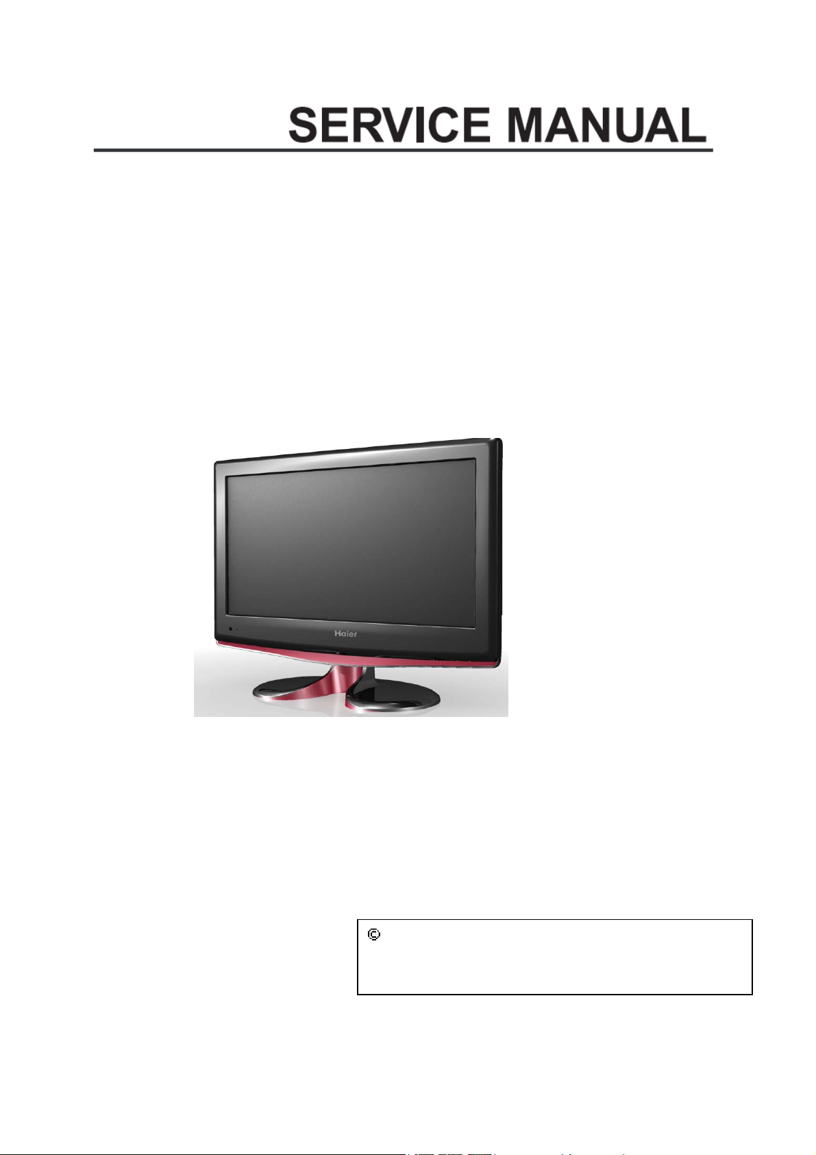
Model No. : HL19KN1
CHASSIS:
COLOR TV
MST721
This service information is designed for experienced repair technicians only and is not designed for use by the general public. It does
not contain warnings or cautions to advise non-technical individuals of potential dangers in attempting to service a product. Products
powered b electricity should be serviced or repaired only by experienced professional technicians. Any attempt to service or repair the
product deal with in this service information by anyone else could result in serious injury or death.
WARNING
2009 (Qingdao Electronics
All rights reserved. Unauthorized copying and distribution is a violation of
law.
1
limited company
)
Page 2

Tableofconents
1.
General Information…………...............……………………………………………………..3
1.1. General Guidelines...………………………………………………………………….. ..3
1.2. Important Notice…………………………………………………………………………..3
1.3. How To Read This Service Manual………………………………………………… .4
2. Speciflcations……………………………………………………………………………..........5
3. Location Of Controls And Components…………………………………...................…......7
3.1Board Location……………………………….. ………………………………….……... .7
3.2 Main Board…………….……………………………….. ………………………………...8
3.3 Power Board……………………………….. …………………………………………...12
3.4 Lcd Panel……………………………….. …………………………………………….…13
4.Disassemble And Assemble………………………………………………………….........…14
5. Installation Instructions…………………………………………………………...................19
6. Operation Instructions…………………………………………………………….............….24
6.1 Front Panel Controls……………………………….. …………………………………....24
6.2 Back Panel Controls……………………………….. ………………………………..…...24
6.3 Universal Remote Controller……………………………….. …..……………………….26
7. Measurements And Adjustments…………………………………………………................27
8. Electrical Parts .………………………………………………………........... .............29
…………………………………………………………………………..………..2
CONTENT
8.1Connetive Wire Photo......................................................................................................29
9. Trouble Shooting……………………………………………………………………………...40
8.2Circuit Diagram................................................................................................................29
2
Page 3

1. General Information
1-1 General Guidelines
When servicing, observe the original lead dress. If a short circuit is found, replace all parts which
have been overheated or damaged by the short circuit.
After servicing, see to it that all the protective devices such as insulation barriers, insulation papers
shields are properly installed.
After servicing, make the following leakage current checks to prevent the customer from being
exposed to shock hazards.
1) Leakage Current Cold Check
2) Leakage Current Hot Check
3)Prevention of Electro Static Discharge(ESD)to Electrostatically Sensitive
1-2 Important notice
1-2-1. Follow the regulations and warnings
Most important thing is to list up the potential hazard or risk for the service personnel to open the
units and disassemble the units. For example, we need to describe properly how to avoid the
possibility to get electrical shock from the live power supply or charged electrical parts (even the
power is off).
This symbol indicates that high voltage is present inside. It is dangerous to
make any king of contact with any inside part of this product.
This symbol indicates that there are important operating and maintenance
instructions in the literture accompanying the appliance
1-2-2. Be careful to the electrical shock
To prevent damage which might result in electric shock or fire, do not expose this TV set to rain or
excessive moisture. This TV must not be exposed to dripping or splashing water, and objects
Filled with liquid, such as vases, must not be place on top of or above the TV
1-2-3. Electro static discharge (ESD)
Some semiconductor (solid state) devices can be damaged easily by static electricity. Such
Components commonly are called Electrostatically Sensitive (ES) Devices. The following
tech-niquesshouldbeusedtohelpreducetheincidenceofcomponentdamagecausedbyelectro
Static discharge (ESD).
1-2-4. About lead free solder (PbF)
This product is manufactured using lead-free solder as a part of a movement within the consum-er
products industry at large to be environmentally responsible. Lead-free solder must be used in the
servicing and repair of this product.
1-2-5. Use the genewing parts (specified parts)
Special parts which have purposes of fire retardant (resistors),high-quality sound (capacitors), low
noise(resistors), etc. are used.
When replacing any of components, be sure to use only manufacture's specified parts shown in
the parts list.
Safety Component
● Components identified by mark have special characteristics important for safety.
3
Page 4

1-2-6. Safety Check after Repairment
Confirm that the screws ,parts and wiring which were removed in order to service are put in the
original positions, or whether there are the portions which are deteriorated around the serviced
places serviced or not. Check the insulation between the antenna terminal or external metal and
the AC cord plug blades. And be sure the safety of that.
Insuration Test
1. Unplug the plug from the AC outlet.
2. Remove the antenna terminal on TV and turn on the TV.
3. Insulation resistance between the cord plug terminals and the eternal exposure metal
should be more than M ohm by using the 500V insulation resistance meter
4. If the insulation resistance is less than M ohm, the inspection repair should be required.
If you have not the 500V insulation resistance meter, use a Tester.
External exposure metal: Antenna terminal Headphone jack
1-2-7. Ordering Spare Parts
Please include the following informations when you order parts. (Particularly the Version
letter)
1. Model number and Version letter
The model number can be found on the back of each product and the Version letter can
be found at the end of the serial number.
2. Part No. and Description
You can find them in your service manual.
1-2-8. Photo used in this manual
The illustration and photos used in this Manual may not base on the final design of products, which
may differ from your products in some way.
1-3. How to read this Service Manual
1-4-1. Using Icons
Icons are used to attract the attention of the reader to specific information. The meaning of each
described in the table below:
Note:
A “note” provides information that is not indispensable, but may nevertheless be valuable to the
reader, such as tips and tricks.
Caution:
A “caution” is used when there is danger that the reader, through incorrect manipulation,
may damage equipment, loose data, get an unexpected result or has to restart(part of)
a procedure.
Warning:
A “warning” is used when there is danger of personal injury.
Reference:
4
icon is
Page 5
A “reference” guides the reader to other places in this binder or in this manual, where
he/she will find additional information on a specific topic.
2. Specification
Model
HL19KN1
Screen size 18.5 inch
Aspect ratio
Brightness
Contrast Ratio
Angel of view
Color display
OSD language
3D decoder
2D comb filter
DNR
3A ENGINE
Same picture split demo(SPD)
double picture demo (DPD)
16:9
400cd/m2
800:1
H170/V160
16.7M
English,
NO
YES
YES
NO
NO
NO
AV stereo
Surrounding sound
NICAM
MUSIC/STANDARD/THEATRE/USE
Bass, Treble
Balance
BBE
LIP SYNC
Equalizer
Earphone
Mute
AV input
DVD terminal
YES
NO
YES
MUSIC/THEATRE/PERSONAL/VOICE
YES
YES
NO
NO
NO
YES
YES
NO
NO
S-video jack
YES
5
Page 6
Y P
B
PR
YES
Monitor out
D-SUB jack
DVI socket
HDMI
SCART jack
Windows Menu
pc automatic adjust
movie mode
Semitransparent menu
ZOOM
16:9 mode
ADVANCED 4:3
PIP
NO
YES
NO
YES
YES
NO
YES
NO
YES
NO
YES
YES
NO
POP
PBP
3A WINDOWS
ATS
Nation Select
Channel List
Input Frequency by Manual and Channel
Number Input
Lock
TELTEXT
NO. of built-in speakers
NO. of outer speakers
Color display
NO. of preset channels
NO
NO
NO
YES
YES
NO
NO
YES
10
2
No
240
100
OSD language
Color system
Audio system
Audio output power(Built-in)(W)
English
PAL/SECA M
DK,BG,I, LL'
1.5W×2
6
Page 7

Audio output power(outer)(W)
No
Total power input(W)
Voltage range(V)
Power frequency(Hz)
Time of sleep timer(MINS)
Net weight(KG)
Gross weight(KG)
Net dimension(MM)
Packaged dimension(MM)
60W
AC150V~AC240V
50~60Hz
240Min
4.67
5.73
471/189/411
530/225/460
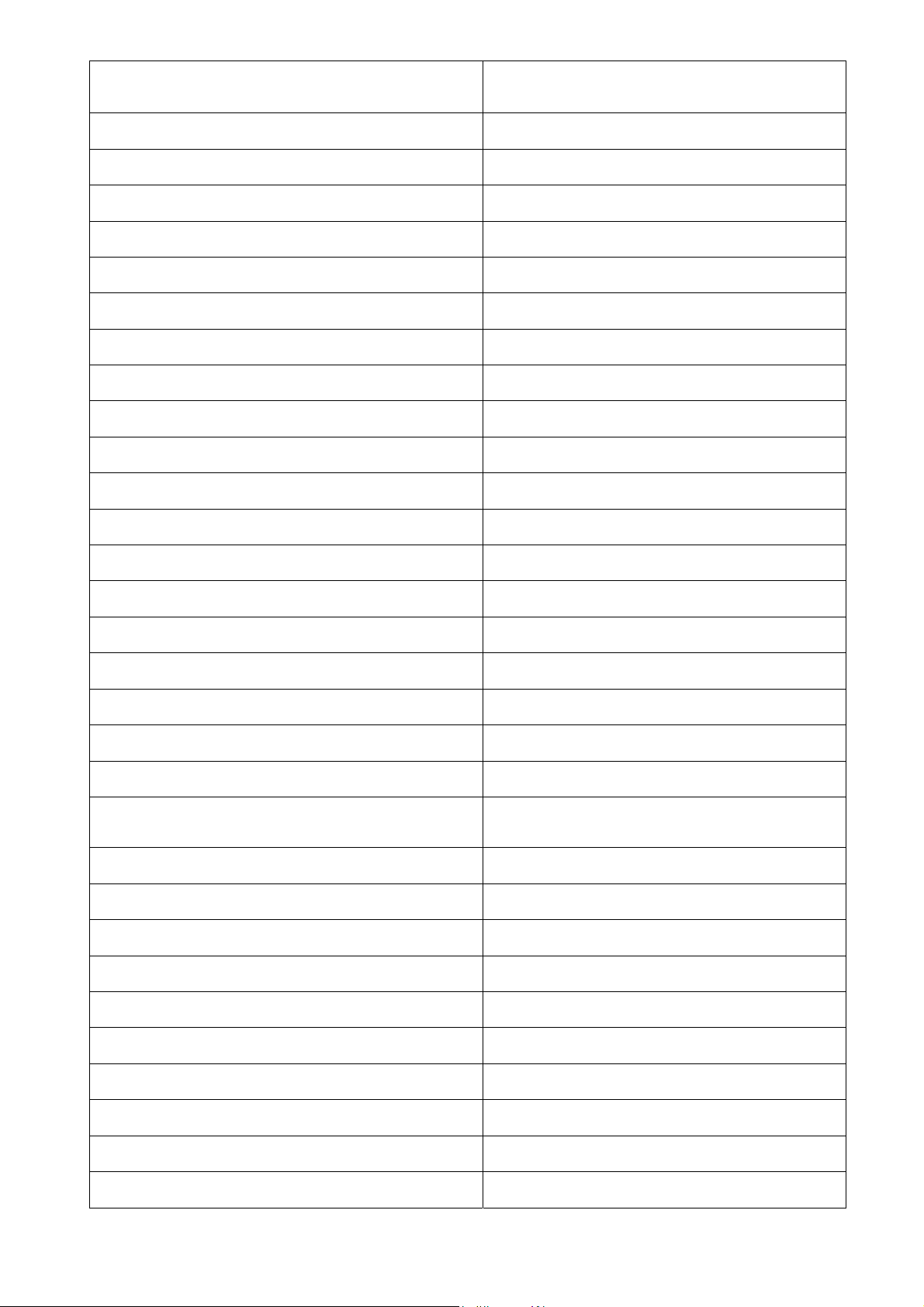
3. LOCATION OF CONTROLS AND COMPONENTS
3.1. Board Location
7
Page 8
No. Parts number Description
A Board
B Board
C
MainBoard Assembly
Power adaptor
Speaker
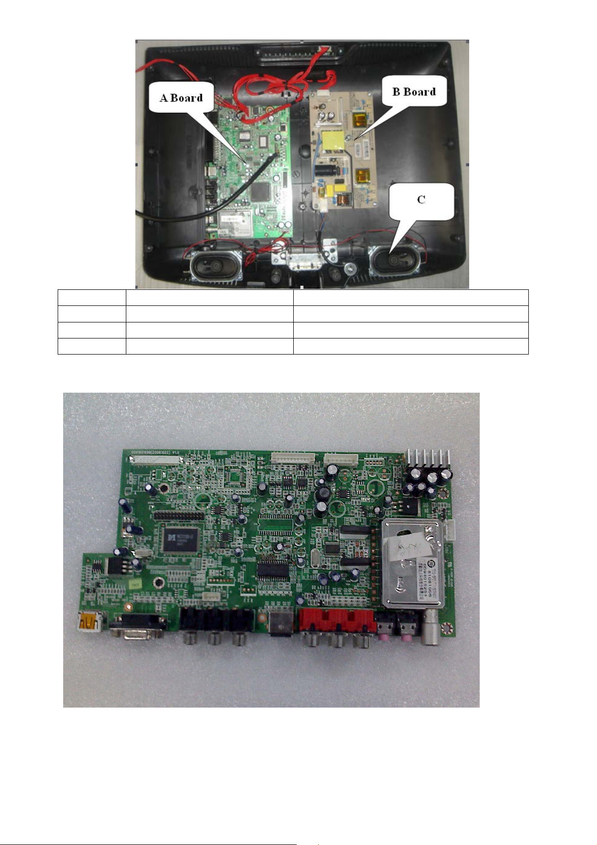
3.2.A.Board----MainBoard
3.2. 1 Function Description:
Main Board:
8
Page 9
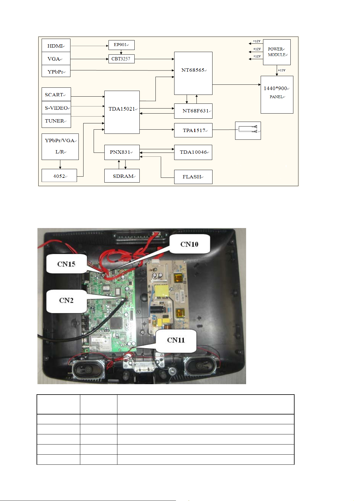
Process signal which incept from exterior equipment,then translate into signal that panel can display.
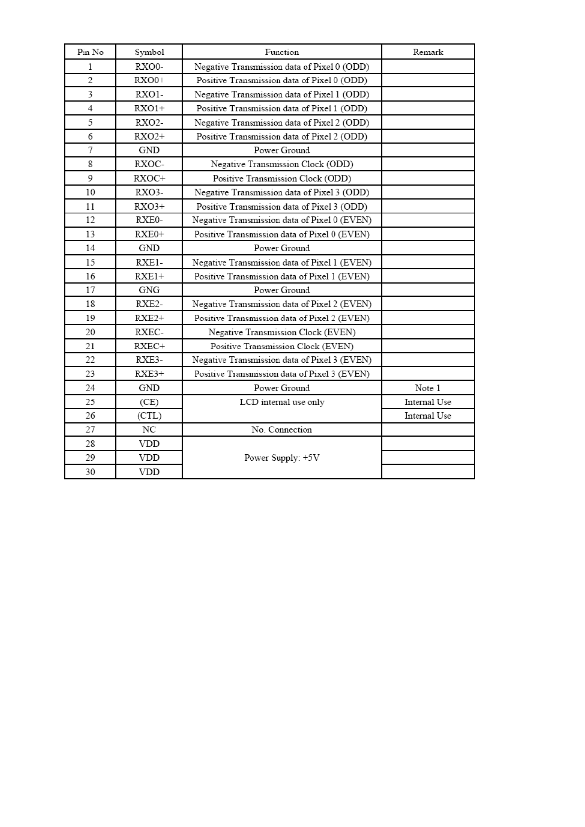
3.2.2 Connector definition
Main board connector
LCDS Connector (CN2)
Signal
Pin number
name Description
1 LCD-VDD
2 LCD-VDD
3 LCD-VDD
4 GND
5 GND
Supply voltage to Panel
Supply voltage to Panel
Supply voltage to Panel
Ground
Ground
9
Page 10
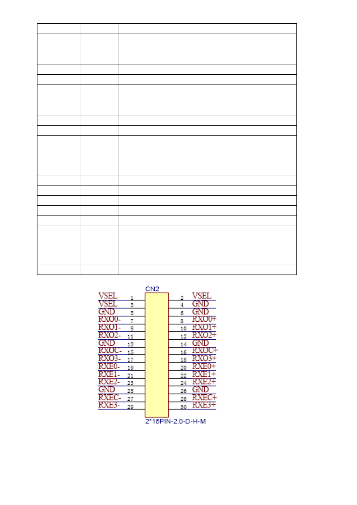
6 GND
Ground
7 RXO0- LVDS ODD 0–Signal
8 RXO0+ LVDS ODD 0 + Signal
9 RXO1- LVDS ODD 1 - Signal
10 RXO1+ LVDS ODD 1 + Signal
11 RXO2- LVDS ODD 2 - Signal
12 RXO2+ LVDS ODD 2 + Signal
13 GND
14 GND
Ground
Ground
15 RXOC- LVDS ODD Clock - Signal
16 RXOC+ LVDS ODD Clock + Signal
17 RXO3- LVDS ODD 3 - Signal
18 RXO3+ LVDS ODD 3 + Signal
19 RXE0- LVDS EVEN 0 - Signal
20 RXE0+ LVDS EVEN 0 + Signal
21 RXE1- LVDS EVEN 1 - Signal
22 RXE1+ LVDS EVEN 1 + Signal
23 RXE2- LVDS EVEN 2 - Signal
24 RXE2+ LVDS EVEN 2 + Signal
25 GND
26 GND
Ground
Ground
27 RXEC- LVDS EVEN Clock - Signal
28 RXEC+ LVDS EVEN Clock + Signal
29 RXE3- LVDS EVEN 3 - Signal
30 RXE3+ LVDS EVEN 3 + Signal
10
Page 11
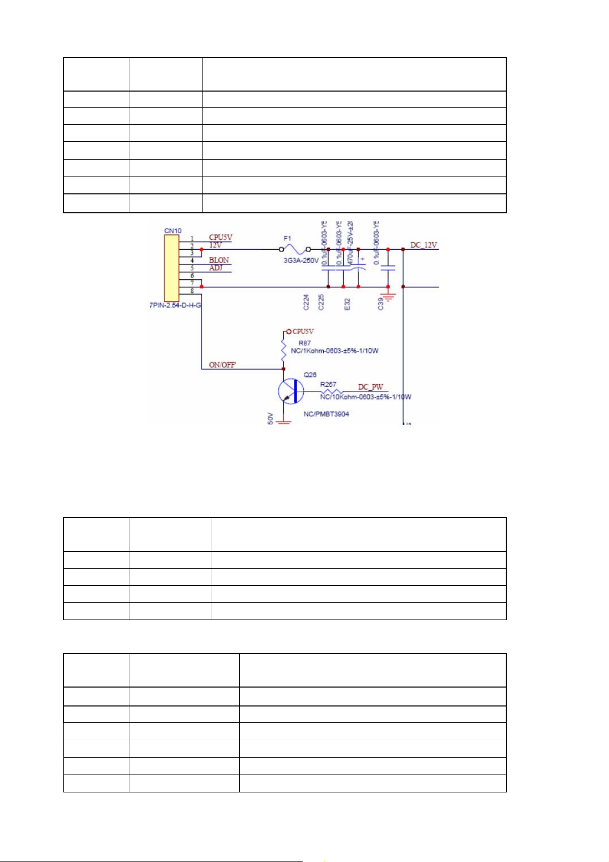
Power supply and Inverter Connector(CN10)
Pin
number Signal name Description
1 ON/OFF Preparative switch control
2 GND
3 GND
Ground
Ground
4 ADJ INVERTER Lightness Adjust
5 BLON INVERTER Switch Control
6 +12V 12V Power
7 +12V 12V Power
Audio Output Connector(CN11)
Pin
number Signal name Description
1 LSPK Left Audio Output
2 GND
3 GND
4 RSPK Right Audio Output
Remote Board and Key board Connector(CN15)
Pin
number Signal name Description
1 IR_IN IR
2 CPU5V 5V Power
3 LED_G Green Indicator light
4 GND
5 LED_R Red Indicator light
6 K6 Key Connector POWER
Ground
Ground
Ground
11
Page 12
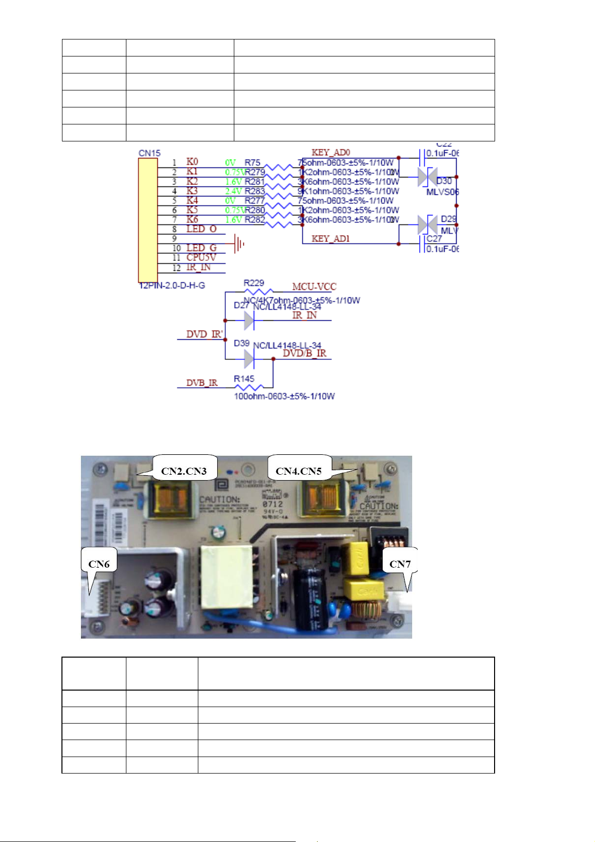
7 K5 Key Connector MENU
8 K4 Key Connector P-
9 K3 Key Connector P+
10 K2 Key Connector V11 K1 Key Connector V+
12 K0 Key Connector SOURCE
3.3B Board-------(Power Board)
Supply power for Main board and Panel
Power supply and Inverter Connector(CN6)
Pin
number Signal name Description
1 ON/OFF Preparative switch control
2 GND
3 GND
Ground
Ground
4 ADJ INVERTER Lightness Adjust
5 BLON INVERTER Switch Control
12
Page 13
6 +12V 12V Power
7 +12V 12V
AC150V~AC240V Input (CN6)
Power supply for panel (CN2. CN3. CN4. CN5.)
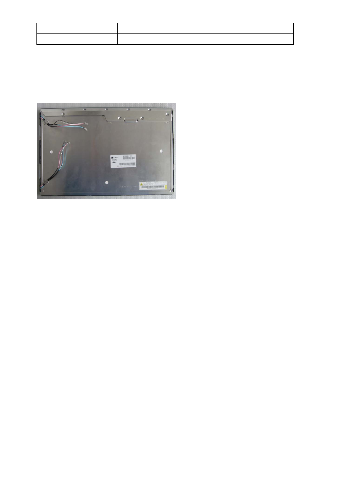
3.4. LCD PANEL.
Power
13
Page 14
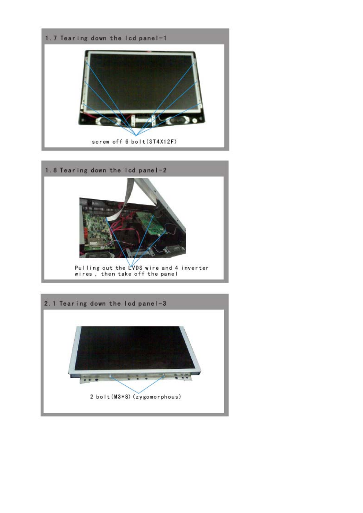
4.DISASSEMBLE AND ASSEMBLE
14
Page 15
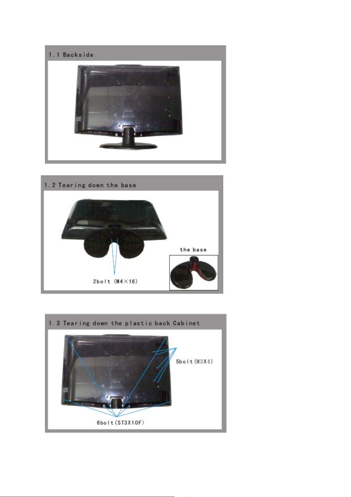
HL19KN1 KNOCKED-DOWN SHOW
15
Page 16
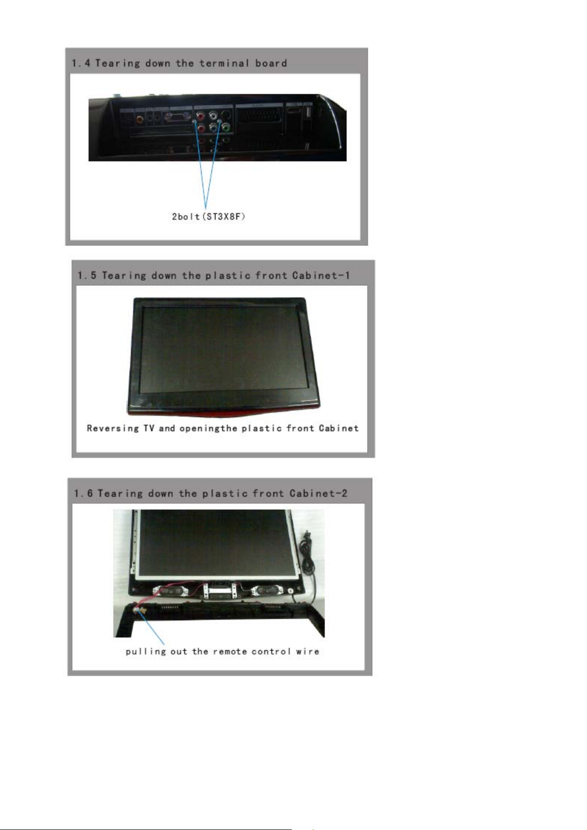
16 17
Page 17
Page 18

18
Page 19

5. INSTALLATION INSTRUCTIONS
Accessories
Remote Control User Manual Battery Audio wire
19
Page 20

20 21 22 23
Page 21

Page 22

Page 23

Page 24

6. OPERATION INSTRUCTIONS
Basal information
6.1 Front panel controls
6.2 Back panel controls
24
Page 25

25
Page 26

6.3 Setting up Your Remote Control
26
Page 27

7. MEASUREMENTS AND ADJUSTMENTS
How to use
The way to the factory mode menu:
1st, press call,
2en, Bond followed by red, green, yellow button
3rd,press call again,
Finished these operations , system will be into the factory mode menu.
useable key:
1.menu: show the next menu page
2.p+/p-: select function
3.v+/v-; set function
27
Page 28

Press the button of OK to quit the factory menu.
28
Page 29

8 Electrical Parts
8.1 Connective Wire Photo
8.2 Circuit Diagram
Page 30

5
4
3
2
1
C1
10nC110n
C10
C10
10n
10n
10uH/4AL210uH/4A
D1
D1
NC/IN4148
NC/IN4148
10uH/4AL510uH/4A
D2
D2
NC/IN4148
NC/IN4148
L2
13
R2
12KR212K
+
+
CA2
CA2
R4
470uF/16V
470uF/16V
2.7KR42.7K
L5
13
R10
R10
12K
12K
+
+
CA7
CA7
R13
R13
470uF/16V
470uF/16V
2.7K
2.7K
5VSTB
CA3
CA3
10uF/16V
10uF/16V
+
+
+5V_DVD
CA8
CA8
10uF/16V
10uF/16V
+
+
C5
0.1uFC50.1uF
C15
C15
0.1uF
0.1uF
+12VU
+3.3V_MST
5VSTB
PANEL-ON/OFF
L1 NC/FBL1 NC/FB
L3 NC/FBL3 NC/FB
L4 FBL4 FB
POWER-ON/OFF
0N 1
OFF 0
PANEL-ON/OFF
0N 1
OFF 0
POWER-ON/OFF
R7
4.7KR74.7K
+12VU
R15
R15
4.7K
4.7K
1
C9
0.1uFC90.1uF
CA4
CA4
220uF/16V
220uF/16V
R5
10KR510K
Q1
2N3904Q12N3904
2 3
L6 FBL6 FB
L7 FBL7 FB
1
+
+
CA9
CA9
10uF/16V
10uF/16V
+
+
2 3
C6
0.1uFC60.1uF
Q2
2N3904Q22N3904
C13
C13
0.1uF
0.1uF
R11
R11
10K
10K
C4
0.1uFC40.1uF
R6
100KR6100K
C14
C14
0.1uF
0.1uF
R14
R14
100K
100K
1
2
3
4
U2
AO4803AU2AO4803A
S1
G1
S2
G2
VCC-Panel
8
D1
7
D1
6
D2
5
D2
+12VA
470uF/16V
470uF/16V
470uF/16V
470uF/16V
1482_ON/OFF
CA1
CA1
CA6
CA6
+12VU
+12VU
R16
R16
4.7K
4.7K
R1 100KR1 100K
+
+
C2
C3
0.1uFC20.1uF
3.9nC33.9n
C7
R3
0.1uFC70.1uF
6.8KR36.8K
R8 100KR8 100K
+
+
C11
C11
C12
C12
0.1uF
0.1uF
3.3n
3.3n
C16
C16
R12
R12
0.1uF
0.1uF
2.2K
2.2K
1
POWER
CON1
CON1
BL-ON/OFF
D D
C C
BRI_ADJ
GND
GND
CON7_2.5
CON7_2.5
DVD_POWER
+3.3V_MST
CON2
CON2
5
4
3
2
1
CON5_2.0
CON5_2.0
12V
12V
NC
R9
4.7KR94.7K
7
6
5
4
3
2
1
DVD_STB
+5V_DVD
+12VA
+12VU
BL-ON/OFF
BL-ADJUST
DVD_STB
+5V_DVD
+12VA
1482_ON/OFF
0N 0
2 3
Q3
2N3904Q32N3904
U1
MP1482U1MP1482
VCC2OUT
7
EN
6
COMP
8
SS
4
GND
U3
MP1482U3MP1482
VCC2OUT
7
EN
6
COMP
8
SS
4
GND
BST
BST
3
1
5
FB
3
1
5
FB
OFF 1
5VSTB
R17
R17
R181KR18
10K
10K
2 3
1K
R191KR19
BL-ADJUST
1K
Q4
2N3904Q42N3904
1
2 3
R21
R21
100R
100R
Q5
2N3904Q52N3904
Title
Title
Title
<Title>
<Title>
<Title>
Size Document Number Rev
Size Document Number Rev
Size Document Number Rev
<Doc>
A3
<Doc>
A3
<Doc>
A3
Date: Sheet of
Date: Sheet of
Date: Sheet of
C18
C18
0.1uF
0.1uF
BL-ON/OFF
C19
C19
2.2uF
2.2uF
1
<RevCode>
<RevCode>
211Thursday, November 27, 2008
211Thursday, November 27, 2008
211Thursday, November 27, 2008
<RevCode>
4
U4
C20
C20
0.1uF
0.1uF
OUT
OUT
2
U4
IN
IN
AMS1084-3.3
AMS1084-3.3
3
+
CA10
+
CA10
47uF/16V
47uF/16V
+3.3V_MST
C17
C17
0.1uF
0.1uF
MST721DU 250mA
+
CA11
+
CA11
47uF/16V
47uF/16V
U5
U5
AMS1117-1.2
AMS1117-1.2
5VSTB5VSTB
4
B B
ADJ
ADJ
1
A A
5
ADJ
ADJ
1
C21
C21
0.1uF
0.1uF
4
OUT
OUT
2
IN
IN
3
+
+
CA12
CA12
47uF/16V
47uF/16V
C22
C22
0.1uF
0.1uF
VCC1.2V
3
正常功耗为
建议先采用
1.25V
MST721DU 150mA
+
CA13
+
CA13
47uF/16V
47uF/16V
0.57W
TO-252
左右
封装
BRI_ADJ
BRI_ON/OFF
BRI_ADJ
BRI_ON/OFF
R22
R22
4.7K
4.7K
R20
R20
4.7K
4.7K
1
2
Page 31

5
4
3
2
1
R24
R24
4.7K
4.7K
ZD4
ZD4
ESD
ESD
R25
R25
4.7K
4.7K
VDDP
DVD_Status
Q6
2N3906Q62N3906
IR_in
ZD5
ZD5
ESD
ESD
AV_out
AV-Lout
AV-Rout
DVD_Status
IR_in
R32 NC/100R32 NC/100
R33 NC/100R33 NC/100
R42
R42
75R
75R
R43
R43
75R
75R
ZD8
ZD8
ESD
ESD
Y-in
C-in
R52
R52
75R
75R
DVD_AUDIO
CON4
CON4
1
2
3
CON3_2.0
CON3_2.0
R38 47RR38 47R
Q7
2N3906Q72N3906
3 2
ZD10
ZD10
ESD
ESD
DVD_L
DVD_R
R3547R R3547R
C25 47nFC25 47nF
C27 47nFC27 47nF
Close to MST IC
R47
R47
10R
10R
R51
R51
10R
10R
1
Q8
2N3904Q82N3904
R53
R53
75R
75R
ZD11
ZD11
ESD
ESD
R61
R60
R60
47K
47K
R61
47K
47K
32
R54
R54
75R
75R
R48
R48
220R
220R
S-Y2Y_DVD
DVD_Lin
DVD_Rin
S-Y2
S-C2
DVD_Lin
DVD_Rin
AV1_Vin+
AV1_Vin-
AV1_Lin
AV1_Rin
R36
R36
10K
10K
R44
R44
10K
10K
R45
R45
47R
47R
R57
R57
10K
10K
R59
R59
10K
10K
R50
R50
47R
47R
C23 47nFC23 47nF
C24 47nFC24 47nF
C26
C26
470pF
470pF
C28
C28
470pF
470pF
Close to MST IC
C29
C29
47nF
47nF
C31
C31
47nF
47nF
C32
C32
470pF
470pF
C33
C33
470pF
470pF
R26 47RR26 47R
ZD1
ZD1
ESD
ESD
C_DVD S-C2
ZD2
ZD2
ESD
ESD
I2C_SCL
I2C_SDA
S-Y1
S-C1
L9FBL9
+5V_Tuner
FB
C30
C30
R49
R49
2.2uF
2.2uF
10k
10k
CA14
CA14
1
47uF/16V
47uF/16V
R55
R55
4.7k
4.7k
CVBS_out
AV-Lout
AV-Rout
DVD_L
DVD_R
AV1
AV1-LinAV-Rout
AV1-Rin
ZD9
ZD9
ESD
ESD
R34 1KR34 1K
ZD3
ZD3
ESD
ESD
R41 1KR41 1K
ZD6
ZD6
ESD
ESD
ZD7
ZD7
ESD
ESD
ZD12
ZD12
ESD
ESD
R581KR58
1K
R29
R29
75R
75R
R31
R31
75R
75R
R46
R46
75R
75R
R561KR56
1K
R30 47RR30 47R
DVD_Y/C
CON3
CON3
D D
CON7_2.0
CON7_2.0
Y_DVD
1
2
C_DVD
3
4
IR_DVD
5
6
7
5VSTB
R23
R23
NC/4.7K
NC/4.7K
R270R R270R
R28100R R28100R
兼容克隆接口
S-video_input
C C
B B
5VSTB
R37
R37
NC/0
NC/0
R39
R39
0/NC
0/NC
P1
P1
3 4
5 7
S-VIDEO-Jack
S-VIDEO-Jack
2PJ-4018-001
2PJ-4018-001
21
6
R40
R40
0/NC
0/NC
AV_input & output
P2P2
9
9
8
7
6
5
4
3
2
1
A A
AV1-Rin
8
7
AV-Lout
6
AV1-Lin
5
4
AV_out
3
2
1
AV1
Title
Title
Title
<Title>
<Title>
<Title>
Size Document Number Rev
Size Document Number Rev
Size Document Number Rev
<Doc> <RevCode>
A3
<Doc> <RevCode>
A3
<Doc> <RevCode>
A3
Date: Sheet of
Date: Sheet of
5
4
3
2
Date: Sheet of
311Tuesday, August 19, 2008
311Tuesday, August 19, 2008
311Tuesday, August 19, 2008
1
Page 32

5
4
3
2
1
Close to Mstar IC
VGA
CN1 VGACN1 VGA
5
15
10
4
14
9
3
13
8
2
12
D D
7
1
11
6
16
17
R62 100RR62 100R
R63 NC/100RR63 NC/100R
R64 100RR64 100R
R65 NC/100RR65 NC/100R
R7775R77
R7575R75
R7675R76
75
75
TXD
VGA_R
VGA_G
VGA_B
HSYNC
ZD15
ZD15
VSYNC
VGA_SDA
VGA_SCL
HSYNC
ZD19
ZD19
VSYNC
R66
R66
R69
R69
10K
10K
10K
10K
ESD
ESD
ZD16
ZD16
ZD18
ZD18
ESD
ESD
ESD
ESD
ESD
ESD
RXD
ZD14
ZD14
ZD13
ZD13
ZD17
VGA_B
VGA_G
VGA_R
75
R78 75RR78 75R
R79 75RR79 75R
R80 75RR80 75R
R68 47RR68 47R
R70 47RR70 47R
R72 47RR72 47R
R74 470RR74 470R
C34
47nF
C34
47nF
C35
47nF
C35
47nF
C36
47nF
C36
47nF
C37
1nF
C37
1nF
C38
47nF
C38
47nF
C39
47nF
C39
47nF
C40
47nF
C40
47nF
VGA-B+
VGA-G+
VGA-R+
VGA-SOG
VGA-R-
VGA-B-
VGA-G-
ZD17
ESD
ESD
ESD
ESD
ESD
ESD
HPD
HDMI_5V
Q9
2N3904Q92N3904
R671KR67
1K
5VSTB
R71
R71
4.7K
4.7K
R73
R73
4.7K
4.7K
HOTPLUG
+5V_VGA
VGA_HSYNC
VGA_VSYNC
VGA_HSYNC
VGA_VSYNC
CEC
R86
R86
100R
100R
M1
2N7002M12N7002
5VSTB
R87
R87
100R
100R
HDMI_CEC
HSYNC
R81 100RR81 100R
VSYNC
R82 100RR82 100R
VGA_SDA
D3
D3
2
3
1
+5V_Tuner
C C
NC/BAT54C
NC/BAT54C
+5V_VGA
VGA_SCL
U6
1
NC
2
NC
3
NC
GND4SDA
NC/24C02U6NC/24C02
VCC
VCLK
SCL
R85
R85
4.7K
4.7K
8
7
6
5
C41
C41
0.1uF
0.1uF
R83 10KR83 10K
R84 10KR84 10K
R89100RR89100R
R88100RR88100R
R90NCR90
NC
VGA_AUDIO
CN2
CN2
PC_PHONE_JACK
PC_PHONE_JACK
CN4
8
7
Y/Pb/Pr
Y/Pb/Pr
CN4
8
7
B B
4
2
1
3
5
6
6
5
5
4
4
3
3
2
2
1
1
ZD26
ZD26
ESD
ESD
PC_L
PC_R
ZD27
ZD27
ESD
ESD
ZD20
ZD20
ESD
ESD
ZD28
ZD28
R115
R115
75R
75R
ESD
ESD
ZD21
ZD21
ESD
ESD
R116
R116
75R
75R
R911KR91
1K
R921KR92
1K
C42
C42
R93
R93
470pF
470pF
10K
10K
Close to Mstar IC
R105 47RR105 47R
R109 47RR109 47R
R112 47RR112 47R
R114 470RR114 470R
R117
R117
75R
75R
ZD36
ZD36
HDMI_5V
ESD
ESD
+5V_Tuner
R96
R96
10K
10K
D16
D16
BAT54C
BAT54C
R97
R97
10K
10K
R98
R98
100R
100R
R101 100RR101 100R
R102 100RR102 100R
R103 10RR103 10R
R104 10RR104 10R
R106 10RR106 10R
R107 10RR107 10R
R108 10RR108 10R
R110 10RR110 10R
R111 10RR111 10R
R113 10RR113 10R
R100
R100
100R
100R
C44
C44
0.1uF
0.1uF
U7
R95
R95
4.7K
4.7K
24C02U724C02
VCC
WP
SCL
SDA
R99 NCR99 NC
GND
1
A0
2
A1
3
A2
4
HPD
HDMI_SDA
HDMI_SCL
CEC
RXCKN
RXCKP
RX0N
RX0P
RX1N
RX1P
RX2N
RX2P
8
7
6
5
VGA_Lin
VGA_Rin
C43
C43
R94
R94
470pF
470pF
10K
10K
ZD22
HPD
HDMI_5V
DDC_SDA
DDC_SCL
CEC
CLK-
CLK+
DAT0-
DAT0+
DAT1-
DAT1+
DAT2-
DAT2+
ZD29
ZD29
ZD22
ESD
ESD
ESD
ESD
HDMI_5V
ESD
ESD
ESD
ESD
ESD
ESD
ZD31
ZD31
ZD30
ZD30
ZD23
ZD23
ZD32
ZD32
ZD24
ZD24
ZD25
ZD33
ZD33
ZD25
ESD
ESD
ESD
ESD
ESD
ESD
ESD
ESD
ZD35
ZD35
ZD34
ZD34
ESD
ESD
ESD
ESD
C45
C45
47nF
47nF
C46
C46
47nF
47nF
C47
C47
47nF
47nF
C48
C48
1nF
1nF
HD_Pr
HD_Pb
HD_Y
HD_SOG
CN3
CN3
CONHDMI
CONHDMI
HPD
GND
DDC SDA
DDC SCL
CEC
CLKClk Shield
CLK+
DAT0-
Dat0 Shield
DAT0+
DAT1-
Dat1 Shield
DAT1+
DAT2-
Dat2 Shield
DAT2+
23
Fin
22
Fin
19
18
+5V
17
16
15
14
NC
13
12
11
10
9
8
7
6
5
4
3
2
1
20
Fin
21
Fin
A A
Title
Title
Title
<Title>
<Title>
<Title>
Size Document Number Rev
Size Document Number Rev
Size Document Number Rev
Custom
Custom
Custom
Date: Sheet of
Date: Sheet of
5
4
3
2
Date: Sheet
VGA&YPbPr&HDMI
<Doc>
<Doc>
<Doc>
<RevCode>
<RevCode>
<RevCode>
of
411Thursday, September 11, 2008
411Thursday, September 11, 2008
411Thursday, September 11, 2008
1
Page 33

5
4
3
2
1
I2C ADDRESS(R263 NC):
24
VIF11VIF2
2
C62
C62
10nF
10nF
22
SIF123SIF2
OUT2
OUT1
3
C65
C65
390pF
390pF
R149
R149
47R
47R
R151
R151
47R
47R
READ is 0X87
WRITE is 0X86
AGND
AGND
C51
C51
R124
R124
1.5nF
1.5nF
330R
330R
21
AFC
FMPLL
4
R1570R157
0
Close to MST IC
AGND
C54NCC54
C53
C53
NC
220nF
220nF
17
18
19
20
VPP
VPLL
CVBS
AGND
DGND7TOP
DEEM
AUD_OUT8SDA
AFD
5
6
C64
C64
C66
C66
470nF
470nF
1nF
1nF
C74
C74
10nF
10nF
C71
C71
47nF
47nF
C72
C72
47nF
47nF
4MHzY14MHz
4
3
16
9
+5V_Tuner
R121
R121
R122
R122
22K
22K
22K
22K
Y1
C50
C50
R126
R126
R125
R125
0.1uF
0.1uF
22K
22K
1 2
C55
C55
22pF
22pF
14
13
15
NC
REF
TAGC
U10
10
R1550R155
0
TV-Vin+
TV-Vin-
U10
TDA9885
TDA9885
SCL
SIOMAD
11
12
R141NCR141
NC
C63
C63
1uF
1uF
AGND
NC(5)/VAGC(6)
R1291kR129
1k
1
100K
100K
AGND
R139 0R139 0
R154NCR154
NC
32
AGND
Q11
Q11
2N3904
2N3904
R135 100RR135 100R
R136 100RR136 100R
R138 100RR138 100R
R142
R142
220R
220R
C52
C52
0.1uF
0.1uF
C58
C58
0.1uF
0.1uF
CA15
CA15
+
+
47UF/16V
47UF/16V
+
CA17
+
CA17
47uF/16V
47uF/16V
R133
R133
75R
75R
IF-AGC
TV-V
SCL
SDA
TV_AUDIO
+5V_Tuner
I2C_SCL
I2C_SDA
TV_AUDIO
TV-SIFP
+5V_Tuner
D D
AGND
U8
TUNER_IFU8TUNER_IF
13
GND114GND215GND312GND4
38MHZ
C56
C56
0.1uF
0.1uF
R148
R148
10R/2W
10R/2W
R152
R152
NC/10K
NC/10K
R156 NC/4K7R156 NC/4K7
AGC1NC12AS3SCL4SDA55VA65VB7NC3833V9NC410IFout
4
U12
U12
IN
GND
IN
GND
OUT
OUT
C692.2uF C692.2uF
C68 0.1uFC68 0.1uF
+
CA18 100uF/16V+CA18 100uF/16V
R153
R153
NC/10K
NC/10K
Q14
Q14
1
NC/3904
NC/3904
2 3
C79
C79
NC/0.1uF
NC/0.1uF
11
R128 0RR128 0R
C59
C59
22pF
22pF
AGND
7805
7805
+5V_Tuner
321
+
C70 NC/0.1uFC70 NC/0.1uF
CA19 100uF/16V+CA19 100uF/16V
Q13
Q13
NC/AO3401
NC/AO3401
1
3 2
IF-AGC TV
R127 10RR127 10R
R130 10RR130 10R
C60
C60
22pF
22pF
L11
L11
NC/100uH
NC/100uH
13
L13 NC/FBL13 NC/FB
+5V_Tuner
C78
C78
0.1uF
0.1uF
SDA
SCL
5VSTB
IF_TV
C73
C73
NC/0.1uF
NC/0.1uF
AGND
R15875R158
75
10nF
10nF
10nF
10nF
C57
C57
R131
R131
4.7K
4.7K
AGND
C61
C61
R134NCR134
NC
AGND
TV-V
L12 FBL12 FB
+5V_Tuner
C C
B B
L10 NC/FBL10 NC/FB
CA16
CA16
47uF/16V
47uF/16V
+
+
+12VA
0N 1
OFF 0
3401_ON/OFF3
A A
3401_ON/OFF
R118
R118
R119
R119
4.7K
4.7K
4.7K
4.7K
D4 792D4 792
Q10
Q10
1
2N3904
2N3904
2 3
AGND
38MHZ
D7
792D7792
R137 NCR137 NC
R143
R143
4.7K
4.7K
AGND
31.5MHZ
1
2
R132
R132
NC/0
NC/0
IN
1
2
ING4OUT1
Q12
Q12
3904
3904
2 3
AGND
IN
ING4OUT1
SAW
SAW
3
AGND+5V_Tuner
R144
R144
4.7K
4.7K
R146 10KR146 10K
1
R147NCR147
NC
D5
792D5792
D6
792D6792
GND
AGND
OUT2
R123
R123
10K
10K
SAW
SAW
3
U11
U11
D6216N
D6216N
AGND
R120
R120
4.7K
4.7K
C49
C49
NC/10nF
NC/10nF
U9
U9
D9455N
D9455N
OUT2
5
GND
5
R145
R145
4.7K
4.7K
AGND AGND
C67
C67
10nF
10nF
R150
R150
75R
75R
R140
R140
5.6K
5.6K
Title
Title
Title
Size Document Number Rev
Size Document Number Rev
Size Document Number Rev
Custom
Custom
Custom
Date: Sheet
Date: Sheet of
5
4
3
2
Date: Sheet of
TUNER&IF
<Title>
<Title>
<Title>
<Doc> <RevCode>
<Doc> <RevCode>
<Doc> <RevCode>
1
of
511Sunday, December 07, 2008
511Sunday, December 07, 2008
511Sunday, December 07, 2008
Page 34

5
IC POWER
+3.3V_MST
FB1FBFB1
FB
C84
C84
C83
C83
0.1uF
0.1uF
2.2uF
2.2uF
+3.3V_MST
+3.3V_MST
VCC1.2V
CON7
CON7
CON4_2.0
CON4_2.0
R202
R202
100K
100K
AVDD_LPLL
FB2FBFB2
FB
C91
C91
0.1uF
0.1uF
AVDD_MPLL
FB4FBFB4
FB
C96
C96
0.1uF
0.1uF
AVDD_12
FB6FBFB6
FB
C98
C98
0.1uF
0.1uF
R189
R189
4K7
4K7
R191
R191
4K7
4K7
5VSTB
R193
R193
4K7
4K7
5VSTB
1
2
RXD
R195 100RR195 100R
3
TXD
R196 100RR196 100R
4
5VSTB
3
2
D8
BAV99D8BAV99
1
R2061KR206
1K
CA21
CA21
2.2uF
2.2uF
D D
C C
LED_CTL
B B
A A
C85
C85
0.1uF
0.1uF
+3.3V_MST
VCC1.2V
R188 200RR188 200R
Q16
Q16
2N3904
2N3904
LED_RED
LED_GRE
Q17
Q17
2N3906
2N3906
R190 200RR190 200R
R194
R194
RX_SCL
TX_SDA
RXD
TXD
1
3 2
4K7
4K7
Q18
Q18
2N3906
2N3906
R209
R209
22K
22K
VDDP
C87
C87
C86
C86
0.1uF
0.1uF
0.1uF
0.1uF
AVDD_33
FB3FBFB3FB
C95
C95
C93
C93
C94
C94
C92
C92
0.1uF
0.1uF
FB5FBFB5
FB
C99
C99
0.1uF
0.1uF
+3.3V_MST
+3.3V_MST
+
CA20
+
CA20
10uF/16V
10uF/16V
R207
R207
100R
100R
5
VDDC
RESET
2.2uF
2.2uF
0.1uF
0.1uF
0.1uF
0.1uF
RXCKN
RXCKP
RX0N
HD_Pb
HD_SOG
HD_Y
HD_Pr
VGA-BVGA-B+
VGA-GVGA-G+
VGA-SOG
VGA-RVGA-R+
VGA_HSYNC
VGA_VSYNC
CVBS_out
RX0P
RX1N
RX1P
RX2N
RX2P
HOTPLUG
HDMI_SDA
HDMI_SCL
S-C1
S-Y1
S-C2
S-Y2
AV1_Vin+
AV1_VinTV-Vin+
TV-Vin-
C100
C100
C97
C97
0.1uF
0.1uF
0.1uF
0.1uF
C110
C110
1nF
1nF
AVDD_33
CLOSE TO MST721DU
CLOSE TO MST721DU
AVDD_33
AVDD_33
R187 390R1%R187 390R1%
C101 0.1u50VC101 0.1u50V
C102 0.1u50VC102 0.1u50V
C103 0.1u50VC103 0.1u50V
CVBS_OUT
4
CRYSTAL
C82
C82
22pF
22pF
50V
50V
12MHZY212MHZ
3
C88
C88
4
22pF
22pF
1 2
Y2
50V
50V
1
2
3
4
5
6
7
8
9
10
11
12
13
14
15
16
17
18
19
20
21
22
23
24
25
26
27
28
29
30
31
32
33
34
35
36
37
38
39
40
41
42
43
44
45
46
SPI FLASH
CE#
SDO
SDI
SCK
4
U13
U13
RXCKN
RXCKP
GND
RX0N
RX0P
AVDD_33
RX1N
RX1P
RX2N
RX2P
HPLUG
REXT
DDC_DA
DDC_CK
HSYNC1
VSYNC1
VCLAMP
REFP
REFM
BIN1P
SOGIN1
GIN1P
RIN1P
BIN0M
BIN0P
GIN0M
GIN0P
SOGIN0
RIN0M
RIN0P
AVDD_33
GND
HSYNC0
VSYNC0
CVBS5P
CVBS4P
CVBS3P
CVBS2P
CVBS1P
VCOM1
CVBS0P
VCOM0
AVDD_33
CVBSOUT
GND
VIN
MST-721
MST-721
R1691MR169
1M
WP_CTL
1
3
5
7 8
PANEL-ON/OFF
POWER-ON/OFF
VDDC
AVDD_LPLL
VDDP
AVDD_MPLL
AVDD_12
153
155
154
156
XIN
XOUT
AVDD_MPLL
FAULTZ47FB2_DPWM48FB1_DPWM49Q251Q1
50
2
RP10
RP10
4
33R
33R
6
152
AVDD_12
AVDD_DPWMADC
R197
R197
33K
33K
143
148
145
149
151
144
147
150
146
141
142
DEO
GND
CLKO
VDDP
VDDC
GPIO[9]
GPIO[6]
GPIO[7]
GPIO[10]
VSYNCO
HSYNCO
MST-721
MST-721
1D/2A/6C Input
1D/2A/6C Input
with CCFL
with CCFL
VDDP
SAR055SAR156SAR2
QOR53GND54MCKO59AMUTE60AUWS61AUSCK62AUSD63SPDIFO64UART1_RX72UART1_TX
58
57
52
VDDP
KEY_1
KEY_0
AU_SCLK
AU_WS
AU_MCLK
R205
R205
NC/10K
NC/10K
C109
C109
0.1uF
0.1uF
1
2
CS
SO
SI
SCLK
SCLK
C113
C113
NC/22pF
NC/22pF
3
VDDP
139
138
140
RA0P
RA0N
VDDP
AVDD_LPLL
65
BRI_ADJ
AU_SD
BRI_ADJ
U16
U16
MX25LV040
MX25LV040
CS
SO
WP
GND4SI
135
137
136
GPIO[13]/RA2P
GPIO[11]/RA1P
GPIO[12]/RA1N
PWMD166PWMD0
VDDC67SCK68SDI69SDO70CSN
VDDC
SCK
VDDP
VCC
HOLD
SCK
133
131
132
134
GPIO[15]/RA3P
GPIO[16]/RA3N
GPIO[14]/RA2N
71
CE#
SDO
SDI
I2C_SCL
FB8FBFB8
FB
8
7
6
5
129
130
GA0P
GA0N
GPIO[17]/GA1P
GPIO[0]74GPIO[3]
73
WP_CTL
I2C_SDA
127
126
125
128
GND
GPIO[19]/GA2P
GPIO[20]/GA2N
GPIO[18]/GA1N
GPIO[1]75GPIO[2]76INT
77
78
DVD_Status
DVD_STB
IR_in
WP
C111
C111
0.1uF
0.1uF
3
GPIO[21]/GA3P
GPIO[22]/GA3N
GPIO[29]
GPIO[30]
BA0P
BA0N
BA1P
BA1N
BA2P
BA2N
BA3P
BA3N
VDDP
RB0P
RB0N
RB1P
RB1N
RB2P
RB2N
RB3P
RB3N
GB0P
GB0N
GPIO[23]/GB1P
GPIO[24]/GB1N
GPIO[25]/GB2P
GPIO[26]/GB2N
GB3P
GB3N
GPIO[27]
GPIO[28]
BB0P
BB0N
BB1P
BB1N
BB2P
BB2N
BB3P
BB3N
VDDC
RESET
CS_CEC
3
2
8
7
6
5
5VSTB
U15
U15
24C32
24C32
VCC
WP
SCL
PWR_ON
C1080.1uC1080.1u
GND4SDA
R204NCR204
NC
R210
R210
4.7K
4.7K
OE
CKV
STV
STH
POL
TP
GVON
GVOFF
B2P
B2N
B1P
B1N
B0P
B0N
G2P
G2N
G1P
G1N
G0P
G0N
CLKP
CLKN
RXO3RXO3+
RXE0RXE0+
BRI_ON/OFF
1482_ON/OFF
3401_ON/OFF
RXE1RXE1+
RXE2RXE2+
RXECRXEC+
RXE3RXE3+
HDMI_CEC
1
A0
2
A1
3
A2
C112
C112
0.1uF
0.1uF
EEP_SCL
EEP_SDA
RXO0-R2P
RXO0+R2N
RXO1-R1P
RXO1+R1N
RXO2-R0P
RXO2+R0N
RXOCRXOC+
VCC-Panel
GVON
GVOFF
+3.3V_MST
R1672KR167
R1682KR168
2K
2K
+3.3V_MST
R1814.7K R1814.7K
1482_ON/OFF
LED_CTL
BRI_ON/OFF
PANEL-ON/OFF
POWER-ON/OFF
WP
BRI_ADJ
AMP-MUTE
13.5V 190mA--250mA
3.3V 110mA
5
CD
4
R263 0R263 0
R264 0R264 0
1
2
3
4
5786
RP20RP2
0
FPC connector for 21.6CMO
FPC connector for 21.6CMO
KEY0_inKEY_0
KEY1_in
R1784.7K R1784.7K
R1794.7K R1794.7K
R1834.7K R1834.7K
R1844.7K R1844.7K
VGH
VGL
XAO
OE
CKV
STV
STH
POL
TP
VDA
VDD
GM1
GM2
GM3
GM4
GM5
GM6
GM7
GM8
GM9
GM10
GM11
GM12
GM13
GM14
CLKN
CLKP
G0N
G0P
G1N
G1P
G2N
G2P
B0N
B0P
B1N
B1P
B2N
B2P
KEY_1
VDD
XAO
5V
C104
C104
560pF
560pF
2
R175 1KR175 1K
R172 1KR172 1K
C89
C89
C90
C90
1nF
1nF
1nF
1nF
IRin
KEY0_in
KEY1_in
ESD
ESD
ESD
ESD
ESD
ESD
ZD39
ZD39
ZD38
ZD38
ZD40
ZD40
R192
R192
10K
10K
U14
U14
S-80937CNMC
S-80937CNMC
1
OUT
2
VDD
VSS3NC
C105 NCC105 NC
R0N
R0P
R1N
R1P
R2N
R2P
1
2
RP1
RP1
3
4
22R
22R
5
6
7 8
R162 22RR162 22R
R163 22RR163 22R
R164 22RR164 22R
R165 22RR165 22R
124
123
122
121
120
119
118
117
116
115
114
113
VDDP
112
111
110
109
108
107
106
105
104
103
102
101
100
99
98
97
96
95
94
93
92
91
90
89
88
87
86
85
GND
84
83
82
GND
81
80
SCL
79
SDA
WP
I2C_SCL
I2C_SDA
R208
R208
4.7K
4.7K
AMP-MUTE
R200
R200
R1994.7K R1994.7K
4.7K
4.7K
R198 100RR198 100R
R201 100RR201 100R
R203 100RR203 100R
U17
U17
24C08
24C08
1
A0
2
A1
3
A2
GND4SDA
VCC
SCL
R211NCR211
NC
EEP_SCL
EEP_SDA
WP
LED_CTL
1482_ON/OFF
3401_ON/OFF
PWR_ON
VDDC
RESET
RX_SCL
TX_SDA
5VSTB
8
7
6
5
IR_in
IR_in
C81
C81
100pF
100pF
R173 470R173 470
R174 1KR174 1K
R176 470R176 470
R177 1KR177 1K
LVDS
R1864.7K R1864.7K
R1824.7K R1824.7K
R1854.7K R1854.7K
CON6
CON6
1
GND
2
VGH
3
GND
4
VGL
5
XAO
6
OE
7
CKV
8
STV
9
NC
10
NC
11
STH
12
POL
13
TP1
14
VDA
15
VDA
16
VDA
17
VDD
18
VDD
19
GND
20
GM1
21
GM2
22
GM3
23
GM4
24
GM5
25
GM6
26
GM7
27
GM8
28
GM9
29
GM10
30
GM11
31
GM12
32
GM13
33
GM14
34
GND
35
R0N
36
R0P
37
R1N
38
R1P
39
R2N
40
R2P
41
CLKN
42
CLKP
43
G0N
44
G0P
45
G1N
46
G1P
47
G2N
48
G2P
49
B0N
50
B0P
51
B1N
52
B1P
53
B2N
54
B2P
55
GND
565657
57
Title
Title
Title
<Title>
<Title>
<Title>
Size Document Number Rev
Size Document Number Rev
Size Document Number Rev
<Doc> <RevCode>
Custom
<Doc> <RevCode>
Custom
<Doc> <RevCode>
Custom
Date: Sheet of
Date: Sheet of
Date: Sheet
1
R160
R160
IRin
R161 10KR161 10K
100R
100R
K6
K2
R171 2kR171 2k
K3
K1
K5
VCC-Panel
RXO0RXO1- RXO1+
RXO2- RXO2+
RXOCRXO3RXE0RXE1RXE2-
RXEC-
RXE3-
VCC-Panel
R249 4.7KR249 4.7K
5VSTB
LED_GRE
LED_RED
K6
K5
K4
K3
K2
K0K4
K1
K0
CON5
CON5
1
2
1
2
3
4
3
4
5
6
5
6
7
8
7
8
9
10
9
10
11
12
11
12
13
14
13
14
15
16
15
16
17
18
17
18
19
20
19
20
21
22
21
22
23
24
23
24
25
26
25
26
27
28
27
28
29
30
29
30
2*20P_2.0mm_HEADER
2*20P_2.0mm_HEADER
DIP15X2-79-V
DIP15X2-79-V
RXO3+
RXO3-
RXOC+
RXOC-
RXO2+
RXO2-
RXO1+
RXO1-
RXO0+
RXO0-
30
29
28
27
26
25
24
23
22
21
20
19
18
17
16
15
14
13
12
11
10
9
8
7
6
5
4
3
2
1
10
11
12
U840
U840
VCC
VCC
VCC
VCC
VCC
GND
GND
GND
NC
SELLCDS
NC
GND
RX3+
RX3GND
RXCLK+
RXCLKGND
RX2+
RX2GND
RX1+
RX1GND
RX0+
RX0GND
NC
GND
NC
GND
NC
C0N30-1.25
C0N30-1.25
CON10
CON10
1
2
3
4
5
6
7
8
9
PH-12A
PH-12A
C8
0.1uFC80.1uF
RXO0+
RXOC+
RXO3+
RXE0+
RXE1+
RXE2+
RXEC+
RXE3+
MST721 BLOCK
of
611Sunday, December 07, 2008
611Sunday, December 07, 2008
1
611Sunday, December 07, 2008
32
31
Page 35

5
4
3
2
1
+5V_Tuner
D D
RP110R RP110R
1
AU_SD
AU_SCLK
AU_WS
AU_MCLK
C C
B B
AV-Lout
AV-Rout
TV_AUDIO
TV_AUDIO
AV1_Rin
DVD_Rin
VGA_Rin
BTSC_L
BTSC_R
VGA_Lin
DVD_Lin
AV1_Lin
R224 1KR224 1K
R226 1KR226 1K
R216 NC/0R216 NC/0
R217 NC/0R217 NC/0
AV1_Rin
DVD_Rin
VGA_Rin
HDMI_Rout
BTSC_L
BTSC_R
HDMI_Lout
VGA_Lin
DVD_Lin
AV1_Lin
2
3
4
5
6
7 8
10nF
10nF
C145
C145
C140 2.2uFC140 2.2uF
C142 2.2uFC142 2.2uF
BTSC_L
BTSC_R
10nF
10nF
C159
C159
C124 1uFC124 1uF
C125 1uFC125 1uF
C126 1uFC126 1uF
C128 1uFC128 1uF
C130 1uFC130 1uF
C132 1uFC132 1uF
C134 1uFC134 1uF
C136 1uFC136 1uF
C138 1uFC138 1uF
C139 1uFC139 1uF
C141
C141
2.2uF
2.2uF
C143
C143
2.2uF
2.2uF
L14FBL14
FB
C1202.2uF C1202.2uF
C114
C114
10uF
10uF
C1210.1uF C1210.1uF
1
2
3
4
5
U18
U18
CS4344
CS4344
1
2
3
4
5
6
7
8
9
10
11
12
13
14
SDATA
DEM/SCLK
LRCK
MCLK
VQ
I2S DAC (option)
C115
C115
0.1uF
0.1uF
9
AOUTLR
VADD
AGND
8
U19
U19
R2S15908
R2S15908
INR5
INR4
INR3
INR2
INR1
INL1
INL2
INL3
INL4
INL5
IGOUTL
VOLINL
IGOUTR
VOLINR
AOUTL
FILT
10
7
6
ROUT
LOUT
TRER
BASSR1
BASSR2
BASSL2
BASSL1
TREL
DGND
SDA
SCL
AGND
REF
VCC
C116 2.2uFC116 2.2uF
C117 2.2uFC117 2.2uF
C122
C122
10uF
10uF
28
27
C127 8200pC127 8200p
26
C129 0.068uC129 0.068u
25
C131 0.068uC131 0.068u
24
C133 0.068uC133 0.068u
23
C135 0.068uC135 0.068u
22
C137 8200pC137 8200p
21
20
19
18
17
+
CA24
16
15
CA24
10uF
10uF
R212 470RR212 470R
R213 470RR213 470R
SDA
R223
R223
100R
100R
SCL
R225
R225
100R
100R
R219
R219
AMP-R
AMP-L
8.2K
8.2K
R222
R222
8.2k
8.2k
C118
C118
470p
470p
I2C_SDA
I2C_SCL
+9VA
C144
C144
0.1uF
0.1uF
C119
C119
470p
470p
R21410K R21410K
R21510K R21510K
HDMI_Rout
HDMI_Lout
R218 10(1/2W)R218 10(1/2W)
R220 220R220 220
CA23
CA23
+
+
NC
NC
9V for Audio
Q19
Q19
2N3904
2N3904
+9VA+12VA
23
R221
R221
NC/0R
NC/0R
1
CA22
CA22
100uF/16v
100uF/16v
D99VD9
9V
A A
Title
Title
Title
<Title>
<Title>
<Title>
Size Document Number Rev
Size Document Number Rev
Size Document Number Rev
<Doc> <RevCode>
Custom
<Doc> <RevCode>
Custom
<Doc> <RevCode>
Custom
Date: Sheet
Date: Sheet of
5
4
3
Date: Sheet of
2
1
of
711Monday, November 24, 2008
711Monday, November 24, 2008
711Monday, November 24, 2008
Page 36

5
4
3
2
1
D D
C C
B B
TDA1517P
AMP-L
AMP-R
+12VU
D10
D10
3
BAV99
BAV99
1
2
R239
R239
CA31
CA31
+
+
2.2M
2.2M
220uF/16V
220uF/16V
0.1uF
0.1uF
C150
C150
R233
R233
2.2M
2.2M
R235
R235
10R
10R
Q20
Q20
2N3906
2N3906
R228
R228
470R
470R
R229
R229
470R
470R
R240
R240
22K
22K
C148
C148
3.3nF
3.3nF
AMP-MUTE7
R236
R236
470R
470R
1
C149
C149
3.3nF
3.3nF
R231 10KR231 10K
2 3
R241 1KR241 1K
+12VA
Q21
Q21
2N3904
2N3904
C146 2.2uFC146 2.2uF
C147 2.2uFC147 2.2uF
L15 FBL15 FB
L16 FBL16 FB
R234
R234
8.2K
8.2K
1
+
+
R232 2.2KR232 2.2K
Q22
Q22
2N3904
2N3904
2 3
470uF/16V
470uF/16V
CA28
CA28
+
+
CA29
CA29
47uF/16V
47uF/16V
U20
U20
TDA1517P
TDA1517P
+
+
CA30
CA30
100uF/16V
100uF/16V
R227
R227
3.3K
20
1
INV1
9
INV2
7
VP
8
M/SS
3
SVRR
GND
GND
2
5
OUT1
GND17GND18GND19GND
OUT2
GND12GND13GND14GND15GND
16
4
6
3.3K
+
+
CA26
CA26
470uF/16V
470uF/16V
+
+
CA27 470uF/16V
CA27 470uF/16V
R230
R230
3.3K
3.3K
CON9
CON9
PHONE_JACK_STEREO_SW
PHONE_JACK_STEREO_SW
4
2
1
3
5
SP_L1
SP_R1
AGND
SP_L1
SP_R2
SP_R1
SP_L2
R242
R242
100(1/2W)
100(1/2W)
SP_L2
SP_R2
CON4_2.5
CON4_2.5
1
2
3
4
CON8
CON8
1
1
M3
1
1
M4
1
HOLE-V8M4HOLE-V8
H6
H6
NC/HOLE-V8
NC/HOLE-V8
1
Title
Title
Title
<Title>
<Title>
<Title>
Size Document Number Rev
Size Document Number Rev
Size Document Number Rev
<Doc>
A3
<Doc>
A3
<Doc>
A3
Date: Sheet
Date: Sheet of
2
Date: Sheet of
811Sunday, December 07, 2008
811Sunday, December 07, 2008
811Sunday, December 07, 2008
1
<RevCode>
<RevCode>
<RevCode>
of
M2
1
HOLE-V8M2HOLE-V8
HOLE-V8M3HOLE-V8
H1
H1
1
5
4
3
2
NC/HOLE-V8
NC/HOLE-V8
A A
5
9
8
7
6
H2
H2
5
4
3
2
NC/HOLE-V8
NC/HOLE-V8
4
H3
1
9
8
7
6
H3
5
4
3
2
NC/HOLE-V8
NC/HOLE-V8
1
9
8
7
6
H4
H4
5
4
3
2
NC/HOLE-V8
NC/HOLE-V8
3
H5
1
9
8
H5
1
7
6
NC/HOLE-V8
NC/HOLE-V8
Page 37

5
4
3
2
1
D D
VCC-Panel
+5V
C154
C154
0.1uF
0.1uF
R245
R245
0805/3.3R/1%
0805/3.3R/1%
U24
U24
3
AT1380
AT1380
C203
C203
270pF
270pF
2
7
C202
C202
NC/0.1uF
NC/0.1uF
OUT
SCP
VCC
IN
FB
OSC
CTL
GND
4
6
R251
R251
200R
200R
1
2N3904
2N3904
2 3
C182 0.1uFC182 0.1uF
R255
R255
3K/1%
3K/1%
VDD
C C
PWR_ON
R1804.7K R1804.7K
R254
R254
10K
10K
走线要尽量短,尽量粗
5
1
8
Q36
Q36
10UH/1.7A
10UH/1.7A
R243
R243
2.2K/1%
2.2K/1%
C151
C151
0.1uF
0.1uF
L27
L27
13
1
R246
R246
10R
10R
C106
C106
100pF
100pF
32
U21
U21
AO3400L
AO3400L
R258
R258
1.8K
1.8K
D14
D14
SK24
SK24
R257
R257
47K
47K
VDA
VDA=0.5X(1+R2/R5)
R244
R244
0805/0R
0805/0R
2
3
2
C155
C155
NC/1uF
NC/1uF
3
U22
U22
NC/AO3401
NC/AO3401
1
1
R250
R250
NC/1K
NC/1K
5V
CA34
CA34
100uF/25V
100uF/25V
C206
C206
+
+
0.1uF
0.1uF
VDA
VDA=0.5X(1+R2/R5)
13.5V
CMO216 190MA-250MA
VCC-Panel
D17
D17
BAV99WPT
BAV99WPT
3
3
D18
D18
BAV99WPT
BAV99WPT
1
C205
C205
1uF
1uF
2
2
C152
C152
1
1uF
1uF
VDA
C156
C156
1uF
1uF
C157
C157
1uF
1uF
R252
R252
10K
10K
R248
R248
100K
100K
R247
R247
20K
20K
2N3906
2N3906
Q23
Q23
2N3906
2N3906
Q24
Q24
12
D13
D13
6.2/BZT52C6V2S-F
6.2/BZT52C6V2S-F
+
+
R2560RR256
0R
CA33
CA33
10uF/16V
10uF/16V
R260
R260
47K
47K
C204
C204
0.1uF
0.1uF
CA35
CA35
+
+
10uF/50V
10uF/50V
R259
R259
0603/0R
0603/0R
VGL
-5.5V 3mA
R253
R253
0603/0R
0603/0R
C153
C153
0.1uF
0.1uF
VGHP
25.6V 10mA
VDA
B B
R2610RR261
0R
Q25
Q25
NC/AO3401
NC/AO3401
2
3
2
VCC-Panel
3
R593
R593
1
CMO216 AMS1117-3.3
4
FOR CMO216 110mA
AMS1117-3.3
AMS1117-3.3
ADJ
OUT
ADJ
OUT
IN
IN
U23
U23
321
C158
C158
+
+
0.1uF
0.1uF
CA37
CA37
47uF/16V
47uF/16V
VDD
R585
R585
NC/10K
NC/10K
32
Q34
Q34
NC/AO3400
NC/AO3400
1
CA36
CA36
C107
C107
+
+
47uF/16V
47uF/16V
0.1uF
0.1uF
GVOFF
NC/560R
NC/560R
R594
R594
NC/2.7K
NC/2.7K
1
NC/AO3400
NC/AO3400
VGHVGHP
R591
R591
NC/1.2K/1%
NC/1.2K/1%
VDD
R590
R590
NC/10K
32
Q35
Q35
NC/10K
1
GVON
A A
Title
Title
Title
<Title>
<Title>
<Title>
Size Document Number Rev
Size Document Number Rev
Size Document Number Rev
<Doc> <RevCode>
A2
<Doc> <RevCode>
A2
<Doc> <RevCode>
A2
Date: Sheet of
Date: Sheet of
5
4
3
2
Date: Sheet
1
of
911Thursday, November 27, 2008
911Thursday, November 27, 2008
911Thursday, November 27, 2008
Page 38

5
D D
4
3
R2671KR267
1K
2
1
C168 0.1uFC168 0.1uF
C169 0.1uFC169 0.1uF
C170 0.1uFC170 0.1uF
C171 0.1uFC171 0.1uF
GM1
GM2
GM3
GM4
GM5
GM6
GM11
GM13
GM10
GM12
GM14
GM7
GM8
GM9
C C
C172 0.1uFC172 0.1uF
C173 0.1uFC173 0.1uF
C174 0.1uFC174 0.1uF
C175 0.1uFC175 0.1uF
C176 0.1uFC176 0.1uF
C177 0.1uFC177 0.1uF
C178 0.1uFC178 0.1uF
C179 0.1uFC179 0.1uF
C180 0.1uFC180 0.1uF
C181 0.1uFC181 0.1uF
GM14
GM13
GM12
GM11
GM10
GM9
GM4
GM3
GM2
GM1
R271 10RR271 10R
R272 10RR272 10R
RP12
RP12
10R
10R
7531
8642
7531
8642
VDA_OP VS7
RP13
RP13
10R
GM8
GM7
GM6
GM5
10R
7531
8642
7531
8642
RP14
RP14
10R
10R
7531
8642
7531
8642
VDA
R287
R287
82.5R/1%
82.5R/1%
B B
R288
R288
10.5K/0.5%
10.5K/0.5%
2
R290
R290
2.55K/0.5%
2.55K/0.5%
R2910R291
0
VREF
1
D15
D15
CA50
CA50
+
+
10uF/16V
10uF/16V
3
LM431/GS431W(A)
LM431/GS431W(A)
VDA
C183
C183
1uF
1uF
VDA_OP
VS14
VS13
38
46
44
37
40
45
43
39
47
1
Mo
2
Lo
3
Ko
4
Jo
5
Io
6
Ho
7
VSS
8
VDD
9
Go
10
Fo
11
Eo
12
Do
48
No
VSS
VDD
Vcomo
Co13NC14VDD15NC16NC17Bo18VSS19Ao20VSS21VDD22Ai23Bi
VDA_OP
U40
U40
Ni
Mi
NC42NC41NC
VSS
VDD
Vcomi
VS12
36
Li
VS11
35
Ki
VS10
34
Ji
VS9
33
Ii
VS8
32
Hi
31
VSS
30
VDD
29
Gi
VS6
28
Fi
VS5
27
Ei
VS4
26
Di
VS3
25
Ci
24
VS2
VS1
VDA_OP
U40.8 U40.15 U40.22 U40.30 U40.43 U40.45
C185
C185
C186
0.1UF
0.1UF
C186
0.1UF
0.1UF
C187
C187
0.1UF
0.1UF
C188
C188
0.1UF
0.1UF
C184
C184
0.1UF
0.1UF
VDA_OP
EC5575/HX8915
EC5575/HX8915
VDA_OP
C189
C189
0.1UF
0.1UF
VREF VREF
R269
R269
1.33K/1%
1.33K/1%
VS1
R273
R273
750R/1%
750R/1%
VS2
R275
R275
1.18K/1%
1.18K/1%
VS3
R277
R277
620R
620R
VS4
R279
R279
360R/1%
360R/1%
VS5
R281
R281
732R/1%
732R/1%
VS6
R283
R283
1.1K/1%
1.1K/1%
VS7
R285
R285
6.2K/1%
6.2K/1%
R270
R270
6.81K/1%
6.81K/1%
R274
R274
715R/1%
715R/1%
R276
R276
R278
R278
R280
R280
665R/1%
665R/1%
R282
R282
1.4K/1%
1.4K/1%
R284
R284
787R/1%
787R/1%
R286
R286
665R/1%
665R/1%
VS8
VS9
825R/1%
825R/1%
VS10
422R/1%
422R/1%
VS11
VS12
VS13
VS14
A A
Title
Title
Title
<Title>
<Title>
<Title>
Size Document Number Rev
Size Document Number Rev
Size Document Number Rev
<Doc> <RevCode>
A2
<Doc> <RevCode>
A2
<Doc> <RevCode>
A2
Date: Sheet of
Date: Sheet of
5
4
3
2
Date: Sheet
1
of
10 11Thursday, September 11, 2008
10 11Thursday, September 11, 2008
10 11Thursday, September 11, 2008
Page 39

5
D D
C C
I2C_SDA
I2C_SCL
+9VA
I2C_SDA
I2C_SCL
+9VA
C196
C196
100nF
100nF
B B
TV-SIFP
C200 220nFC200 220nF
CA47 4.7uF/16V
CA47 4.7uF/16V
TV-SIFP
+
+
4
R292
R292
8.2K
8.2K
R293
R293
150
150
C191 47nC191 47n
+
+
CA39 10uF/16V
CA39 10uF/16V
+
+
CA42 4.7uF/16V
CA42 4.7uF/16V
R295 100R295 100
C197 2.2uFC197 2.2uF C198 15nFC198 15nF
+
+
CA45 100uF/16V
CA45 100uF/16V
C201
C201
470n
470n
R296 2.2KR296 2.2K
+
+
CA49 10uF/16V
CA49 10uF/16V
1
2
3
4
5
6
7
8
9
10
11
12
13
14
15
16
U26
U26
VEO
VEI
C-NR
C-M
C-DEC
AGND
DGND
SDA
SCL
VCC
COMP
V-CAP
C-P1
C-P2
C-PH
C-ADI
TDA9850T
TDA9850T
3
C-S
C-W
C-TS
C-TW
MAD
OUTL
C-ND
C-L
Vref
SAP
C-SDE
OUTR
C-R
C-SS
C-MO
CER
32
31
30
29
28
27
26
25
24
23
22
21
20
19
18
17
C190 1uFC190 1uF
C192 1uFC192 1uF
CA40 10uF/16V
CA40 10uF/16V
CA41 10uF/16V
CA41 10uF/16VC193 100nFC193 100nF
C194 100nFC194 100nF
C195 2.2uFC195 2.2uFR294 100R294 100
CA43 100uF/16V
CA43 100uF/16V
C199 2.2uFC199 2.2uF
C207 2.2uFC207 2.2uF
C208 2.2uFC208 2.2uF
C209 2.2uFC209 2.2uF
C210 2.2uFC210 2.2uF
2
+
+
+
+
BTSC_L
+
+
BTSC_R
BTSC_L
BTSC_R
1
1 2
X1 500KX1 500K
A A
Title
Title
Title
Size Document Number Rev
Size Document Number Rev
Size Document Number Rev
Date: Sheet of
Date: Sheet of
5
4
3
Date: Sheet
<Title>
<Title>
<Title>
<Doc> <RevCode>
A
<Doc> <RevCode>
A
<Doc> <RevCode>
A
of
11 11Thursday, September 11, 2008
11 11Thursday, September 11, 2008
2
11 11Thursday, September 11, 2008
1
Page 40

9.Trouble shooting
Power supply trouble
1、Power supply trouble
Check (F1/3A) for 12V?
N
Y
Check F1 and peripheral power supply Check E33/470μF/16V for 5V
N
F1 is damaged?
NY
Turn on the TV-set(By button or
remote control)
N
Y
LDO(U10,U13,U16,U18,U19,
Were those
etc.)worked normal?
Check power
OK
supply net
follow F1
Check U6/MCU
1:Power supply(U7、U9))
2:Reset signal
3:Crystal
Change U1/MP1410ES-LF or
D17/SK34A-SMA
Check U1 for 5V
output
YN
Check L9/47μH
LDO was damaged
or the loader is in
short circuit
Y
YN
OK
It’s normal but the
voltage is high
Check Pin No.4 of
U1/MP1410-ES or
change U1
It’s normal but the
voltage is Low
E33 was damaged
or the loader is in
short circuit
Page 41

Power supply trouble (DVB--T)T)
Power supply trouble (DVB
2
、
Check E43/470μF/16V for 5V
N
Check U15 Pin 3 for 12V pulse
Y
L16 open
or
damaged
NO 12V
Check The PCB board isn`t
open or in short circuit from
F1 to U15 Pin 2
N
Check U15 Pin
NO.2 for 12V
input,Pin
NO.7 for 3.3V
NO 3.3V
Check U6/MCU Pin NO.
5 for 3.3V output
Or change U6/MCU
U22 is
damaged
and
change it
N
Check U22
for 5V
input
Y
Check
U22
output
is in
short
circuit
N
Y
1 U22 is damaged and
change is。
2 Check the back
circuit
Check U22
(AIC1084-
33PM)for
3.3V output
N
Check the
circuit
before
U22
Check U34
for 1.2V
output
Check U34
for 3.3V
input
Y
Check
U34
isn`t in
short
circuit
N
Y
Y
Y
N
Y
U34 is damaged and
change it
Check
U32 and
change
it
1 U34 is damaged and
change is。
2 Check the back circuit
Check U32
(AZ1117H
-1.8)for
1.8V output
N
Check U32
for 5V
input
N
Check
U32
Front
Circuit for
power
supply
Page 42

Display trouble(exceptional
screen)
Y N
Check if the LCD
panel is ok
NY
Exceptional screen
Check if the cable is correct
and connected tightly
Change LCD
Check the circuit of output and
the CN2/Jack
Y
Check the power supply for
U5 and the clock circuit
N
Change or repair the
Damaged components
Change the cable for
Panel connector
Page 43

Display trouble(white screen)
NY
White screen
Check the power supply
for panel
Check the switch signal for
Q24/AO3401(changed
Check CN8 or change Q24
from 5~0V)
NY
Check the circuit from U6/NT68F631 to Q24
or U6 had been damaged
Check the output signal
Of U5
Y
Change the LCD panel or
The cable to panel
N
Check U5
Page 44

Display trouble(black screen)
Black screen
The voltage of BLON Signal
is 5v? (on CN10 )
Check if the inverter is
NY
Change the inverter
Y
working normal?
Check the power
supply for TV set
N
Check R25/22 ohm or change U6
Page 45

Audio trouble(No sound)
N
No sound
Check if have audio input signal
Y
Check the set of volume
and MUTE
Check the
audio
source
N
Reset it
Y
Check the
speaker
Check the circuit
from U6-pin2,30 to
U3-pin8 or U6 had
been damaged
Check U3-pin8 voltage≥9.2V
Y
Check if U3-pin4,6 have
audio signal output
N
Change U3
Check the output
circuit from U3
and CN23
Y
Check CN11 output
signal
Y
Check if U3-pin1,9 have
audio signal input
Y
Check audio input signal:
PC/SV/YPBPR:U21-pin53,54
SCAR:U21-pin56,57
YN
Check U21pin45 for 8V
or change
U21
N
Check U3/TPA1517NE-pin7
for power supply >11V
YN
N
Check if U21-pin60,61
have audio signal output
N
Check the
net between
audio input
jack and
U21
N
Y
Check the
Power supply
Circuit for
U3
Check the
net between
U21-pin60,61
And U3-pin1,9
Page 46

Function trouble
(TV video)
N
TV cann’t searched any channel/no picture
Confirm if the RF cable
does have signal
Check T1/VA1Y1ED2002
Check T1-pin4,5 for I2C
Y
Check T1-pin8 for signal
Pin7for 5V?
Y
Y
N
N
Check
external
RF
Signal
source
Y
Check the
circuit from
T1-pin8to
U21-pin24,25
and the power
supply for U21
TCheck T1pin1for
voltage 1.8~4.3V
changeT1
N
Check the circuit
NY
Check I2C circuit
(U6/NT68F631
PIN16,17)
Check the
power
supply
circuit
Page 47

Display trouble(exceptional
screen)
TV no audio but picture
The same as in PC and YPBPR mode?
Y
If there was signal on
Pin2 of SAW2/AF389A2D?
YN
N
Refer to ”6”
1. Change SAW2
2. Examine PIN No.29,30 of U21
3. Examine the power supply for
U21
4. Change U21
1.Check the circuit
between SAW2/pin2
and C133/0.01μF
2.change C133.
Page 48

Function Trouble (PC)
PC
Picture not
In center
Do “Auto adjust”
process
Missing
color
Check the R.G.B
input signal for U5
YN
Do “Reset“ process
on the menu
Check the circuit
of R.G.B
input
Picture
dithering
Check if the wave
of Vsync,Hsync is ok
Y
Do “Reset“ process
on the menu or
the input mode
cann’t be support
N
Check the
circuit of
Vsync,Hsync
No signal
Check the circuit
of Vsync,Hsync
or there was no
signal input
Page 49

Function Trouble (Scart,HDMI,YPBPR)
SCART RGB、HDMI 、YPBPR 、 SCART Video、S- Video
No signal
Check the circuit of
VSYNC and HSYNC
signal
Missing
color
Check the input signal of R.G.B
to U5
YN
Check R.G.B circuit
(If on scart channel,
Reset
should check the
input circuit of
SCART R.G.B)
PC/HDMI/YPBPR mode
No signal besides
Check the power
Supply for U21
Page 50

Audio (HDMI no sound trouble)
Check U14 Pin1,2,3,4those signal input
•
Check if U12 and RP12 are
mounted firmly
N
Check U12 power supply and
if CN18 is mounted firmly?
N
Y
N
Y
Remount
Y
Check U14/CS4344 power
supply is worked normal?
NY
Check U14/
CS4344 power supply
Check U14 circuit
Change U12
Check U12 circuit
Or remount
Page 51

Function Trouble (DVB-T)
DVB can’t find any channel/no picture
N
DVB can’t find any channel/no picture
Power supply worked normal?(U15,U22,U32,U34)
Check
the
power
supply
circuit
Y
Check U25Pin37 is 3.3V?
N
Check 3.3V
power
supply circuit
Check the reset circuit
Y
(U6 Pin42 to U25
Pin12)
Y
Check Pin6 of T1 has 4M clock signal?
Check T1-pin4,5 for I2C
Or T1 damaged
Check the reset signal of U25
N
Y
U25 damaged
Y
Check power supply for U30
N
OK
Check whether there is TS-
Stream output from U30 to U26
N
U26/TDA100
46A or
RP17,RP16,
RP9 weren’t
mounted
firmly or
damaged
/PNX8316
Damaged and
Y
U26
change it
NG
Check the
power supply
circuit
Page 52

Function Trouble (DVB-T)
DVB No sound
DVB no sound
CheckU26’s Pin202,203,204 output signal?
N
Y
Remount
Check if U29’s Pin1,2,3 have audio signal input
Check if the input circuit were
mounted firmly
N
U29’s input circuit has damaged
Y
N
Y
Check if U29’s Pin6,9 have audio output
N
Check 5V supply for U29 ?
OK
Change U29
U26’s audio out pin had short circuited?
N
Y
Check the circuit of audio output
Check power supply for
U26(PNX8316HS/102)
Or change U26
Page 53

Y
Pb
Pr
Y
Pb
Pr
TUNER
DTV_R
DTV_G
DTV_B
DVD-Y
DVD-C/Cb
CON12V
DVD5V
YP AUDIO LI
YP AUDIO RI
HD AUDIO LI
HD AUDIO RI
PC AUDIO LI
PC AUDIO RI
DVD AUDIO LI
DVD AUDIO RI
HDMI DATA
VGA_SCL
VGA_SDA
VGA_R
VGA_G
VGA_B
VGAVS
VGAHS
ADDR
IF
VT SEL0
CVBS IN
AV/SV AUDIO LI
AV/SV AUDIO RI
SV-Y IN
SV-C IN
SCART VI
SCART LI
SCART RI
SCART SW
SCART FB
SCART RIN
SCART GIN
SCART BIN
SCART VO
SCART LO
SCART RO
HD_SCL
HD_SDA
DTV AGC
ATV AGC
TUN 5V
SDA_TUN
SCL_TUN
IFN
IFp
24C08
ATV AGC
FB0.4V
BUFFER
BUFFER
BUFFER
4052
HDCP SDA
HDCP SCL
DVD_Y
DVD_PB
DVD_PR
Y
Pb
Pr
VT SEL1
AUDIO
SAW
VIDEO
SAW
DTV IIS
DTV_CVBS/Y
DTV_C
DTV G/DVD-Y
DTV B/DVD-C
DTV R
DTV_LI
DTV_RI
VT SEL0
VT SEL1
AV/HD/YP LI
AV/HD/YP RI
WAKE UP
D1V8 D3V3
SCL_TUN
SDA_TUN
DTV AGC
TDA1004X
IFN
IFp
HD_3V3
HD RST
SCL
EP901
HD Y
HD Pb
HD Pr
CBT3257
OP2
SDA
IIS
VT SEL1
CS4334
TVR
TVG
TVB
TDA150XX
FLASH SDRAM
VGAVS
CPU 5V
VGAHS
Pr/RIN
Y/GIN
Pb/BIN
TVR
TVG
TVB
TV VS/
TV HS/
5V
HD AUDIO LI
HD AUDIO RI
74LVC14CBT3257
TV HS
TV VS
24C16
VGA_SDA
VGA_SCL
TXD
RXD
WAKE UP
MUTE
AMP STB
PW_DN
HPD CON
HPD DET
HD_SCL
HD_SDA
CPU 5V
UOC_SCL
UOC_SDA
UOC_REQREAD
UOC_READYCOMM
UOC_REQCOMM
U_DC 5V
U_8V
U_1V8
U_3V3
RESET
CON12V
D SCL
D SDA
T RESET
TS
SCL
SDA
SCL
SDA
MUTE
NT68565
NT68F631
MUTE
IRQ
SC RST
CON12V
&POP REDUCE2
POP REDUCE1
TPA1517
AMP STB
STANDBY
D1V2 D3V3
PNX831X
SINGLE TTL
SINGLE/DUAL LVDS
DC 5V
PNL 3.3V
DC12V
S_1V8
S_3V3
BL PWM
A/DTV SW
PNL PWR
BAKLIGHT
KEY_AD0
KEY_AD1
LED GRN
LED RED
CPU 5V
IR
MCU_3V3
K0
K1
K2
K3
K4
K5
K6
K7
DVD 5V
D5V
DVD/DTV IR
SDA_TUN
SCL_TUN
OSD CON1
DVD_ON
EP RST
UR133L
DVD ON
DTV IIS
DVD/DTV IR
OSD CON
A/DTV SW
TXD/RXD
PANEL
MCU_5V
CON12V
BUFFER
DAC
INVERTER
DC12V
DCDC
DCDC
78L05
AO3401
DTV_CVBS/Y
DTV_C
DTV_R
DTV_G
DTV_B
DTV IIS
DTV_LI
DTV_RI
D_1V2
D_3V3
D_1V8
DC_12V
PW_DN
HD_3V3
U_3V3
U_1V8
S_3V3
PNL 3.3V
DC 5V
PW_DN
DC_12V
PW_DN
8V
Page 54

FACTORY MENU ADJUSTMENT
FACTORY 1
GAIN (White balance value ;0-255)
R 128
G 128
B 128
OFFESET (Black balance value ;0-255)
R 128
G 128
B 128
CONTRAST (0-63)
R 0
G 0
B 0
DECODER
BRIGHTNESS (0-63)
CONTAST (0-63)
YC DELAY
PAL 0-15
NTSC 0-15
SECAM 0-15
AUTO (Adjust white blance auto)
SAVE
FACTORY 2
VIDEO(PC colour temperature ;0-255)
R 128
G 128
B 128
AGC 30
DCXO -120
DISC 0
AUTO (Ajust Nicam ,DISC set up to from 125 to 129)
AUTO POWER OFF/ON (When push AC SWITCH ,TV turn on
automatically or not)
AUTO BURNING OFF/ON(When push AC SWITCH ,TV enter burning mode
or not)
INIT EEPROM >(Initiate EEPROM and TV standby)
Page 55

SAVE >
FACTORY 3
STANDARD/MILD/FRESH(Ajust picture mode)
BRIGHTNESS 50
CONTRAST 50
SATURATION 50
VOLUME 0-63(Max volume)
DVD MODE OFF/ON
SECAM L/L’ OFF/ON
NICAM OFF/ON
TELETEXT OFF/ON
LOCK SET OFF/ON(Hotel Lock function)
FIRST SEARCH OFF/ON(Auto search or not when first poweron)
HDMI OFF/ON
AV OFF/ON
SCART OFF/ON
COMPONENT OFF/ON
LANGUAGE EC/EU8/ER(Language selection)
CHANNEL TAB QD/JN(Factory signal tab)
NO SYNC TIME 5M/10M(Standby time when no signal for five
minutes or ten)
SAVE >
3.Use the MENU key to switch FACTORY 1,FACTORY 2 and FACTORY 3 and use
the EXIT key to exit factory menu.
Page 56

Sincere Forever
71
 Loading...