

Page 1
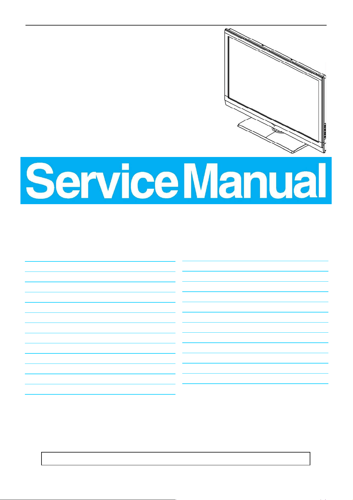
18.5Ǝ LCD TV Haier HL19D2
Service
Service
Service
Horizontal Frequency
31~68 KHz
TABLE OF CONTENTS
Description Page Description Page
Table of Contents.......……....................................…........1
Important Safety Notice.......................................……......2
Revision List…………………………………………………3
1. General Specification.................................………........4
2. Operating Instructions…………………….……...….......6
2.1 The Use of Remote Control…….…………...…….......6
2.2 To Use the Menus…...………………….….………......7
2.3 Front Panel Control Knobs……………….………......12
2.4 How to Connect…….…………………….…..…….....13
3. Input/Output Specification…………....................…....14
4. Mechanical Instructions…………………….................16
5. Repair Flow Chart ……………………….…….…….....20
6. PCB Layout ………………..………………....…..........25
6.2 Power Board…..…………..………….…..…….......28
6.3 Key Board………………………..……..……….......30
6.4 IR Board…………………………..……….…….......30
7.Adjustment..............................................................31
8.Block Diagram.…….................................................32
9.Wiring Diagram.……...............................................34
10.Schematic Diagram………..……..………………...35
10.1 Main Board…………….…………………...….......35
10.2 Power Board………..…....…………...……….......48
10.3 Key Board……………….………….………….......50
10.4 IR Board……………………………….……….......51
11.Exploded View……………………….………….…...52
12.BOM List……………….…………………………….54
6.1 Main Board………………..……………...…….….......25
SAFETY NOTICE
ANY PERSON ATTEMPTING TO SERVICE THIS CHASSIS MUST FAMILIARIZE HIMSELF WITH THE CHASSIS
AND BE AWARE OF THE NECESSARY SAFETY PRECAUTIONS TO BE USED WHEN SERVICING
ELECTRONIC EQUIPMENT CONTAINING HIGH VOLTAGES.
CAUTION: USE A SEPARATE ISOLATION TRANSFOMER FOR THIS UNIT WHEN SERVICING
1
Page 2

Important Safety Notice
Proper service and repair is important to the safe, reliable operation of all Haier Company Equipment. The service
procedures recommended by Haier and described in this service manual are effective methods of performing
service operations. Some of these service operations require the use of tools specially designed for the purpose.
The special tools should be used when and as recommended.
It is important to note that this manual contains various CAUTIONS and NOTICES which should be carefully read in
order to minimize the risk of personal injury to service personnel. The possibility exists that improper service
methods may damage the equipment. It is also important to understand that these CAUTIONS and NOTICES ARE
NOT EXHAUSTIVE. Haier could not possibly know, evaluate and advise the service trade of all conceivable ways in
which service might be done or of the possible hazardous consequences of each way. Consequently, Haier has not
undertaken any such broad evaluation. Accordingly, a servicer who uses a service procedure or tool which is not
recommended by Haier must first satisfy himself thoroughly that neither his safety nor the safe operation of the
equipment will be jeopardized by the service method selected.
Hereafter throughout this manual, Haier Company will be referred to as Haier.
WARNING
Use of substitute replacement parts, which do not have the same, specified safety characteristics might create
shock, fire, or other hazards.
Under no circumstances should the original design be modified or altered without written permission from Haier.
Haier assumes no liability, express or implied, arising out of any unauthorized modification of design.
Servicer assumes all liability.
FOR PRODUCTS CONTAINING LASER:
DANGER-Invisible laser radiations when open AVOID DIRECT EXPOSURE TO BEAM.
CAUTION-Use of controls or adjustments or performance of procedures other than those specified herein may
result in hazardous radiation exposure.
CAUTION -The use of optical instruments with this product will increase eye hazard.
TO ENSURE THE CONTINUED RELIABILITY OF THIS PRODUCT, USE ONLY ORIGINAL MANUFACTURER'S
REPLACEMENT PARTS, WHICH ARE LISTED WITH THEIR PART NUMBERS IN THE PARTS LIST SECTION OF
THIS SERVICE MANUAL.
Take care during handling the LCD module with backlight unit
-Must mount the module using mounting holes arranged in four corners.
-Do not press on the panel, edge of the frame strongly or electric shock as this will result in damage to the screen.
-Do not scratch or press on the panel with any sharp objects, such as pencil or pen as this may result in damage to
the panel.
-Protect the module from the ESD as it may damage the electronic circuit (C-MOS).
-Make certain that treatment person’s body is grounded through wristband.
-Do not leave the module in high temperature and in areas of high humidity for a long time.
-Avoid contact with water as it may a short circuit within the module.
-If the surface of panel becomes dirty, please wipe it off with a soft material. (Cleaning with a dirty or rough cloth may
damage the panel.)
2
Page 3

Revision List
Version Release Date Revision Instructions Model
A00 Feb.27,2010 Initial release E19A4ZNK3WH3NN
3
Page 4
1. General Specification
* This model complies with the specifications listed below.
* Designs and specifications are subject to change without notice.
* These models may not be compatible with features and/or specifications that may be addedin the future.
Model No. HL19D2 HL24XD2 HL32D2 HL42XD2
DISPLAY
Viewable 18.5W" 23.6W" 31.5W" 42W"
Television System NTSC standard,ATSC standard (8-VSB, Clear-QAM)
VHF: 2 through 13
UHF: 14 through 69
Cable TV: Mild band (A - 8 through A - 1,A through I),
Channel Coverage
Tuner input (75ȍ)
AV IN: AV/S-Video and L/R audio input
PC IN:D-SUB and PC Audio (Headphone mini-jack)
Supported scan rate: 640x480@60/72/75Hz,720x400@70Hz,
1280x1024@60Hz,1440x900@60Hz,1680x1050@60Hz
Super band (J through W),
Hyper band (AA through ZZ,AAA, BBB),
Ultra band (65 through 94, 100 through 125)
CONNECTIONS
800x600@56/60/72/75Hz,1024x768@60/70/75Hz,
1280x720@60Hz,1280x768@60Hz
1360x768@60Hz:For HL19D2 / HL32D2 only.
1920x1080@60Hz: For HL24XD2 / HL42XD2 only.
Rear Connectors Recommended: For HL19D2 / HL32D2: 1360x768
For HL24XD2 / HL42XD2: 1920x1080
Component Video and L/R Audio input
Supported resolution: 480i,480p,720p,1080i,1080p
HDMI input Supported scan rates: 480i, 480p, 720p, 1080i, 1080p
AV/S-Video input
AV/S-Video input
SPDIF
HDMI HDMI HDMI 2 HDMI 2
Side Connectors
Earphone Output
USB PORT
AV/S-Video input
SPDIF
Earphone Output
USB PORT
SPDIF
HDMI 1
Audio out Audio out
AV IN 2
Earphone Output
USB PORT
AV/S-Video input
SPDIF
HDMI 1
AV IN 2
Earphone Output
USB PORT
4
Page 5
Model No. HL19D2 HL24XD2 HL32D2 HL42XD2
WEIGHT & DIMENSIOIN
Dimensions 457.3 mm 572.2 mm 790.5 mm 1015.36 mm
with Stand 324.8 mm 407.6 mm 569.1 mm 703.03 mm
(W x H x D) 171.29 mm 176.8 mm 239.6 mm 280.50 mm
Dimensions 457.3 mm 572.2 mm 790.5 mm 1015.36 mm
without Stand 308 mm 372.8 mm 526.8 mm 654.67 mm
(W x H x D) 67.1 mm 65.4 mm 91.1 mm 97.10 mm
Weight with Stand 4.25 Kg 5.75 Kg 12.5 Kg 20.5 Kg
Weight without Stand
and Base
VESA-compatible
wall bracket 100 x 100 mm 100 x 100 mm 200 x 200 mm 400 x 200 mm
(W x H)
Screw type Metric 4 x 10 mm Metric 4 x 10 mm Metric 6 x 10 mm Metric 6 x 10 mm
3.85 Kg 5.4 Kg 10.6 Kg 17.6 Kg
WALL MOUNTING
POWER
Power Consumption 45W 70W 150W 250W
Standby <1W
Mains Power 120V~60Hz
Audio Power 3W + 3W 3W + 3W 10W + 10W 10W + 10W
Ambient Temperature
Supplied Accessories
English
5°C - 35°C
PACKAGE CONTENTS
TV unit x1
Base x1
Screws x 4 (for 32” only)
Power cord x 1
Remote control x1 (with two size AAA alkaline batteries)
User manual x1
FCC statement x1
Registration Card x1
5
Page 6
2. Operating Instructions
ġ,Ģ
⦼,⦽
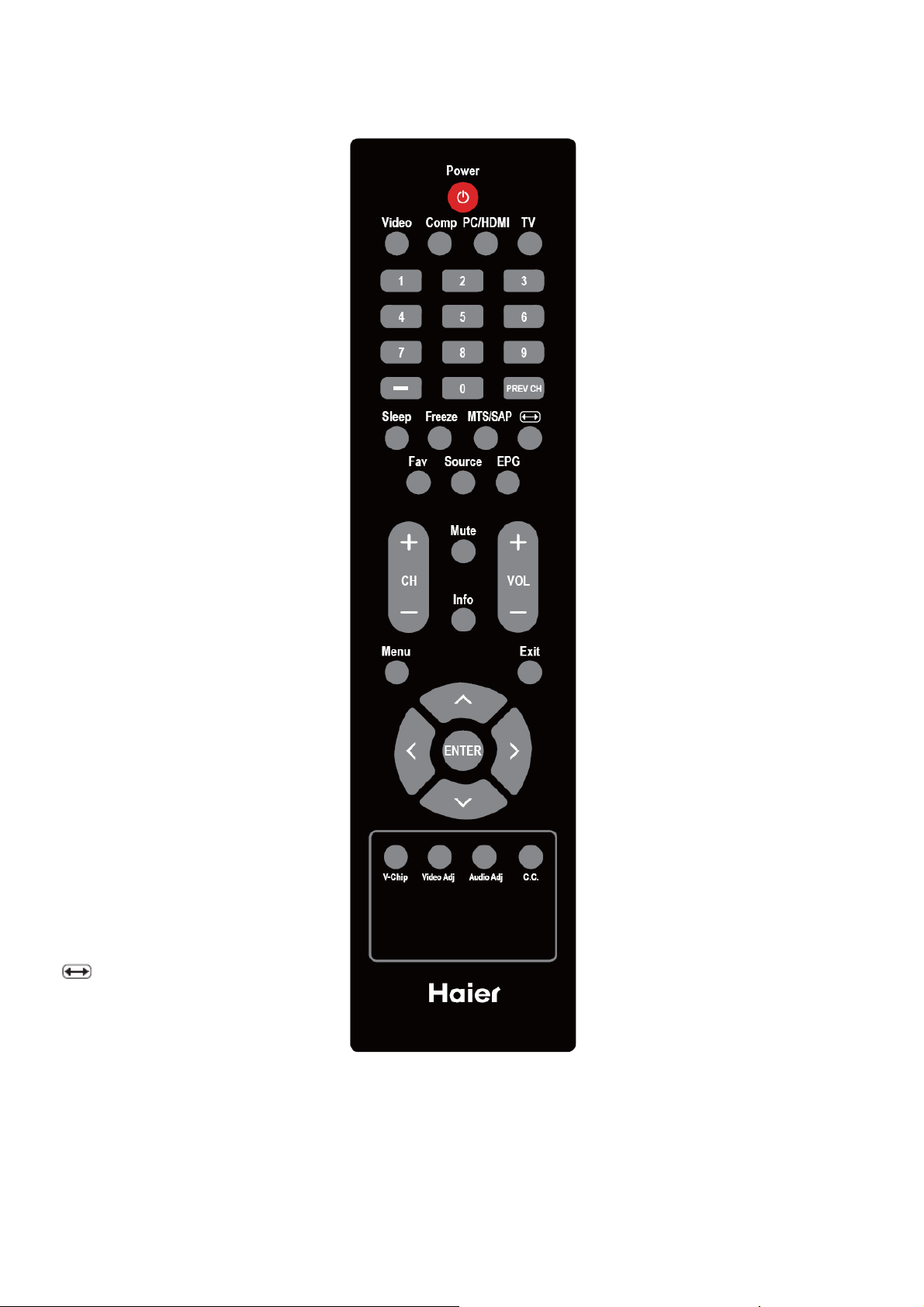
2.1 The Use of Remote Control
Power
Press to power ON/OFF(standby) TV.
(Note: 1. TV is never completely power
off unless physically unplugged. 2.
Press to turn on TV after the power on
status, LED had changed to blue and
stopped flashing.)
Video
Press repeatedly to choose
S-Video/Composite source mode.
Comp
Press to choose Component source
mode.
PC/HDMI
Press repeatedly to choose VGA
or HDMI source mode.
TV
Press to choose ATSC/NTSC TV
source mode.
0 ~ 9 / – number
Press to enter TV channel number to
select channel (Press ‘-’ to choose the
sub-channel).
PREV CH
Press to display the previous channel.
Sleep
Press to set the preset time to switch
the TV to standby mode automatically
(off / 5 / 10 / 15/ 30 / 60 / 90 / 120 / 180
/240 mins).
Freeze
Press to freeze the displayed picture.
MTS/SAP
Press to activate the NTSC TV sounds,
such as: Stereo, SAP or Mono tone, and
languages of DTV.
Wide
Press to choose the display aspect as:
Normal, Zoom1, Wide, Zoom2, or HDMI
PC mode.
Fav
Press "Fav" to open or toggle channel
item in Favorite Channel List.
Source
Press repeatedly to choose the various
input sources.
EPG
Press to display the Electronic Program
Guide.
CH+ / CH -
Press + or - to browse through the TV
channels.
Mute
Switch the sound ON/OFF.
Info
Press to show the information about the
input source, TV channel, display
resolution and current time.
VOL+ / VOL
Press + or - to adjust the volume.
Menu
Press to open or exit menu.
,
, ENTER
Press to adjust the various function
items on the menu.
Exit
Press to exit menu or OSD.
V-Chip
Press to lock Parental Control
temporarily. (After setting the restricted
table of MPAA or TV Rating.)
Video Adj
Provide video modes switching.
Audio Adj
Provide audio modes switching.
C. C.
Press repeatedly to change the
closed caption type as CC On/CC
Off/CC On With Mute.
6
Page 7
2.2 To Use the Menus
1. Press the Menu button to display or close the main menu.
2. Use the Navigation Ring to move around to select, adjust or confirm an item in the OSD (On Screen Display)
menu.
Press the Menu button to enter the main OSD. Adjust the items including Video menu,Audio menu, Feature menu,
Channel menu, and VGA menu. However, some function items in the menus may only be enabled in the particular
source modes.
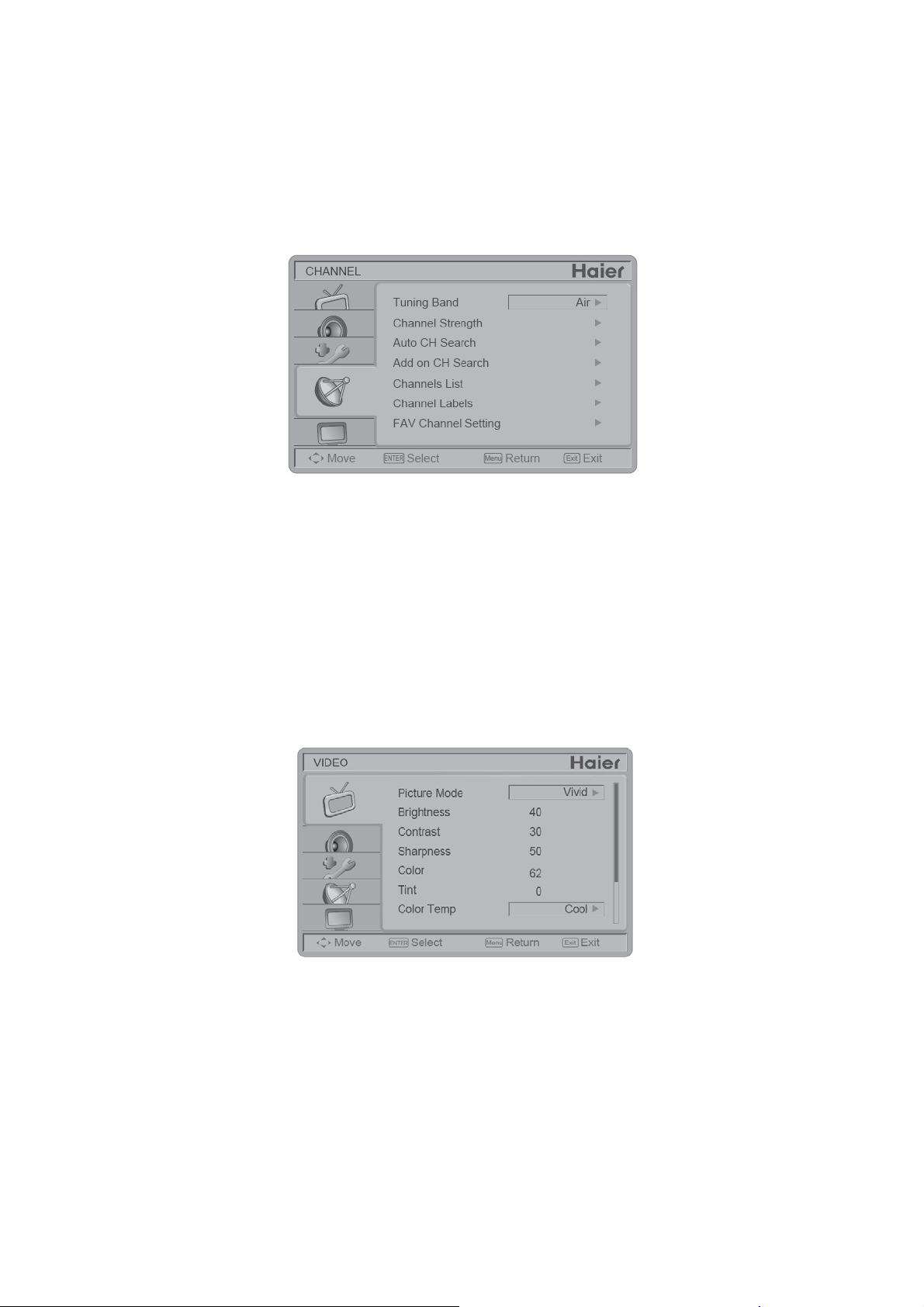
CHANNEL MENU
The Channel menu in TV mode shows as below.
1. Tuning Band: Select TV source signal from the Air (antenna) or Cable (CATV).
2. Channel Strength: Show the intensity of the received DTV signal.
3. Auto CH Search: Automatically scan all NTSC / ATSC TV channels and then store in the channel table. In channel
scan process, the OSD can display the number of channels which had been found.
4. Add on CH Search: Add channels which are new found.
5. Channel List: Show the Channel List. User can edit (add/delete) the channel numbers.
6. Channel Labels: Show the NTSC / ATSC TV Channel Labels menu for user modifying channel labels specifically.
7. FAV Channel Setting: Show the Favorite Channel List. User can edit (add/delete) the favorite channels.
VIDEO MENU
The Video menu in most source modes shows as below. It provides several video adjustment items for user fine
tuning the video display.
Only in VGA source mode, the Video menu simply provides Picture mode, Color Temp, Backlight, Aspect Ratio,
Preset items.
1. Picture Mode: Adjust the best picture appearance from selecting the preset value of Vivid, Standard, Eco, Movie,
or Personal.
2. Brightness: Video brightness adjustment, the tuning range is 0 ~ 100.
3. Contrast: Video contrast adjustment, thetuning range is 0 ~ 100.
4. Sharpness: Video sharpness adjustment,the tuning range is 0 ~ 100.
5. Color: Video color chroma adjustment,the tuning range is 0 ~ 100.
6. Tint: Video tint adjustment, the tuning range is R50 ~ G50.
7. Color Temp: Three color temperature modes. (Normal / Warm / Cool)
8. Noise Reduction: Gives four NR effect degrees, such as: Low, Mid, High and Off.
9. Adaptive Contrast: Choose On or Off to adjust the gamma after analyzing the input signal automatically.
10. Backlight: Backlight strength adjustment,the tuning range is 0 ~ 30.
11. Aspect Ratio: Choose the display aspect: Normal, Zoom1, Wide, Zoom2, or HDMI PC mode.
12. Preset: Restore the default video settings.
7
Page 8
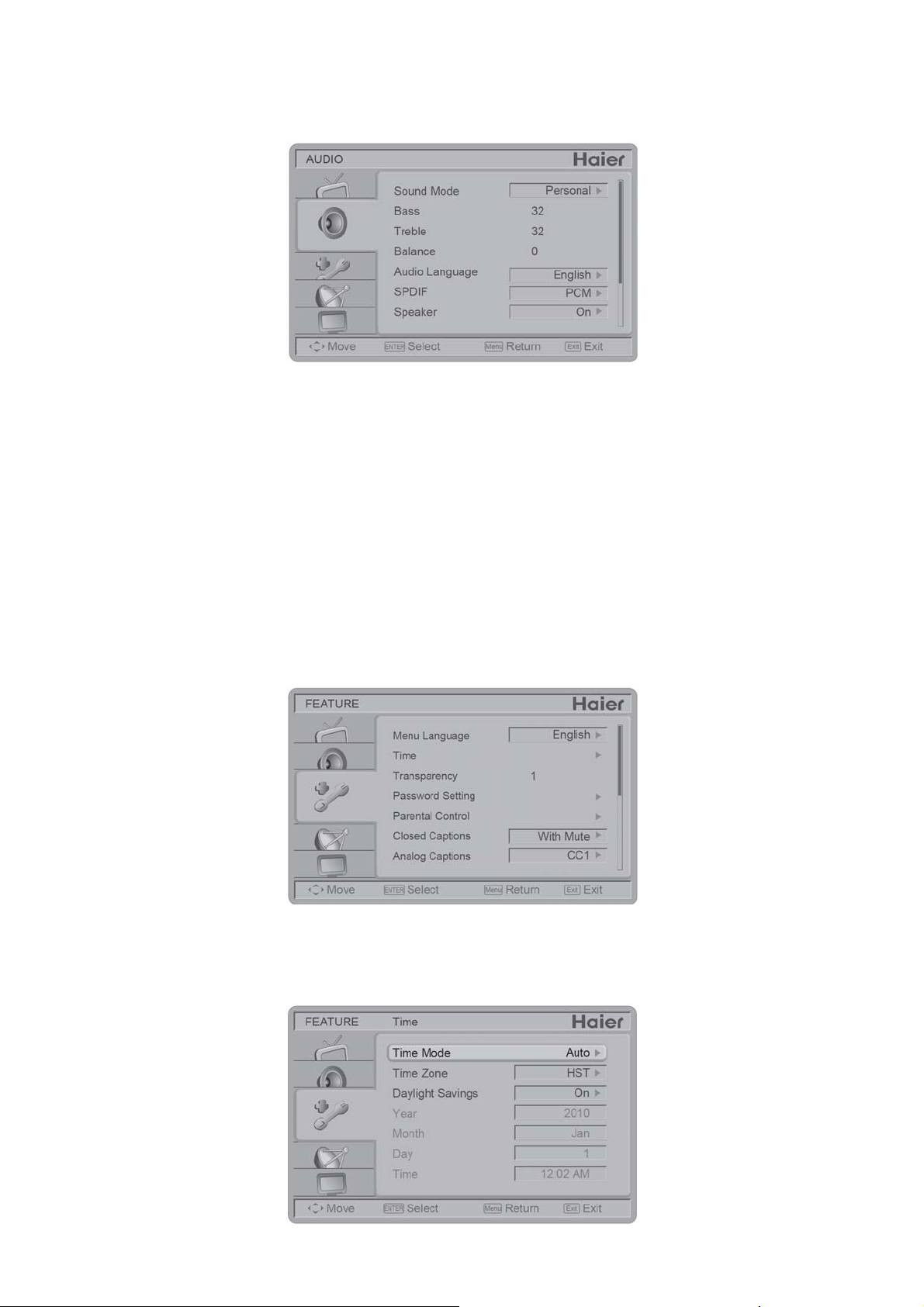
AUDIO MENU
The Audio menu in TV mode shows as below.
It provides audio adjustment for user to modify the audio setting. Audio language setting is only available with ATSC
TV source, the option is disable under other source modes.
Sound Mode: Choose the audio mode: Personal, Music, or Speech.
2. Bass: Bass tone adjustment, the tuning range is 0 ~ 63. (The default state is enabled.)
3. Treble: Treble tone adjustment, the tuning range is 0 ~ 63. (The default state is enabled.)
4. Balance: Audio balance adjustment, the tuning range is L50 ~ R50.
5. Audio Source: Select the audio source from Mono, Stereo, or SAP. (This function works in ATV only.)
6. Audio Language: Change the audio language setting on ATSC TV programs. The number of the supported
audio languages depends on the ATSC TV programs. (English / Français / Español)
7. SPDIF: Digital audio output format. Select from RAW and PCM. (This function works in DTV only.)
8. Speaker: Choose to turn on / off the TV internal speaker. The digital audio output signals and earphone output
signals will not be turned off even though the TV speaker is off. The default setting is On.
9. AVL: Choose On or Off to adjust volume to be consistent across programs and channels automatically.
10. Preset: Restore the default audio settings.
FEATURE MENU
The Feature menu in TV mode shows as below.
This menu gives users the most flexibility to satisfy their generally demands. According to the various requirements
in different source modes, certain features should be hidden (disable) on the menu. The detailed footnotes will be
described clearly below.
1. Menu Language: Select the menu display language. (English / Français / Español)
2. Time: Set current time. The sub-menu includes Time Mode, Time Zone, and Daylight Savings.
[Time Mode] ů Choose from Auto or Manual.
[Time Zone] ů Set current time zone.
[Daylight Savings] ů Set to On or Off.
8
Page 9
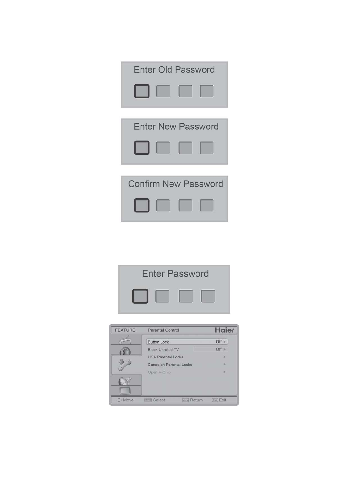
3. Transparency: Adjust the transparency of the on-screen menu from range 0 to 10.
4. Password Setting: Change the 4-numeral parental control password. Three steps are
required for changing the password: Enter Old Password -> Enter New Password ->Confirm New Password. Note:
This item is only available in TV, Composite and S-Video source modes. The default password is ό0 0 0 0ύ.
5. Parental Control: Provide the parental Control (V-chip) function setting. Before entering the Parental Control
sub-menu, user has to key in the password first. Enter the Parental Lock item, then the user can
modify the restricted table about MPAA or TV Rating respectively. While exiting the sub-menu, the parental control
function is working. The inhibitive channels or source signals can be unlock through key in the correct password.
Note: This feature is only available in TV, Composite and S-Video source modes.(The default password is: 0 0 0 0.)
[Button Lock] – Select On or Off to lock or unlock the control buttons on the side panel of the TV. When this
function enables, the control buttons on your TV will be locked and TV only can be controlled by remote control only.
[Block Unrated TV] – When Block Unrated TV is set to on, your TV will block unrated program.
[USA Parental Locks] – Set the parental control level by MPAA or TV Rating.
[Canadian Parental Locks] – Set the parental control level by English Rating or French Rating.
[Open V-Chip] – Open V-Chip is an advanced V-Chip rating system for digital channels that are received.
The rating table will be updated by downloading the RRT5 data for blocking.
9
Page 10
6. Closed Captions: Select a closed caption options. (Off / On / With Mute)
7. Analog Captions: Select an analog caption options. (CC 1-4 / TEXT 1-4)
8. Digital Captions: Select a digital caption options. (SERVICE 1-6)
9. Digital Captions Setup: Provide numerous options for setting the digital closed caption style in the sub-menu.
[Style] – Set to Automatic or Customer mode. If Custom mode is selected, user can modify the detail styles
described below. The setting result will be shown immediately on the bottom of the submenu OSD. Note: This
feature is only available in Digital TV (ATSC) mode.
[Size] – Digital closed caption font size, which can be set as Automatic, Small, Normal, or Large.
[Font] – Digital closed caption font style,which can be chosen as Automatic, Default,or Font 1 ~ 7.
[Text Color] – Automatic / White / Red / Green / Blue / Yellow / Magenta / Cyan / Black.
[Text Opacity] – Automatic / Solid /Flashing / Transparent / Translucent.
[Background Color] – Automatic /Black / White/ Red / Green / Blue / Yellow /Magenta / Cyan.
[Background Opacity] – Automatic /Solid / Flashing / Transparent / Translucent.
[Edge Effect] – Automatic / None/ Raised / Depressed / Uniform / Left / Shadow / Right Shadow.
[Edge Color] – Automatic / Red / Green / Blue / Yellow / Magenta / Cyan / Black / White.
10. Input Labels: User can edit the input labels.
11. Component Setting: This option only shows and is available in component mode,which provides fine tuning
component display.
[Phase] – Adjust Picture Phase to reduce Horizontal-Line noise. The tuning range is from 0 to 31.
[Preset] – Restore the default component setting values.
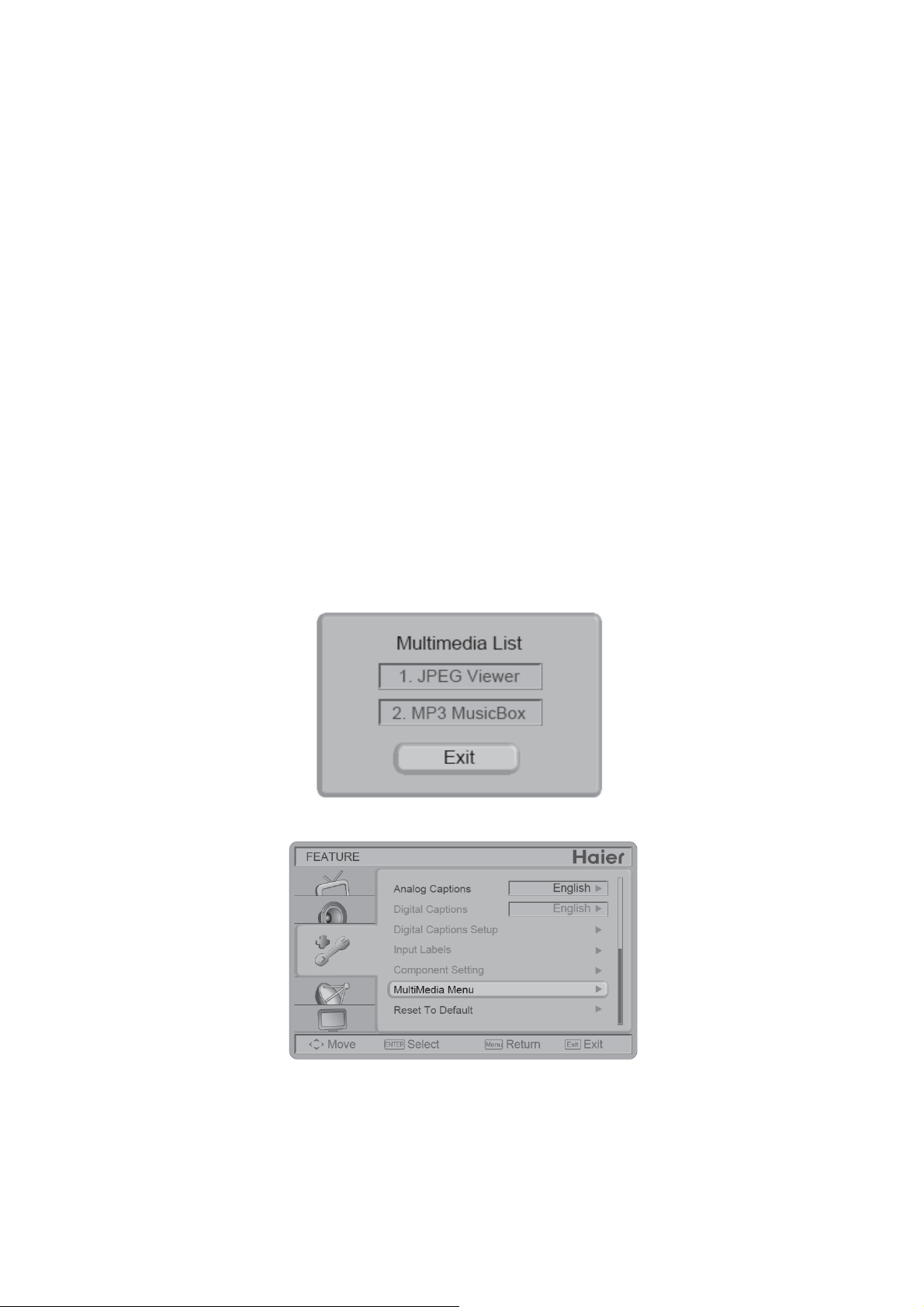
12. MultiMedia Menu: This option shows the photos in JPEG formats and plays the music in MP3 formats that stored
in a USB storage device.Note: File number is limited to 1000 files.
JPEG sizes are limited as followed:
For 19"/32": 10928x6114
For 24"/42": 15360x8640
There are two ways to enter JPEG Viewer and MP3 MusicBox interface:ŻŻ After plugging USB storage device into
USB hub, Multimedia List menu will display.
Ż Select MultiMedia Menu in Feature Menu to choose JPEG Viewer or MP3 MusicBox. These two items are
activated only if the USB storage device is plugged into the USB hub.
[JPEG Viewer] ů Press Menu to display control menu. Press Enter to enlarge the selected photo (orange frame) in
browser.
Ż Image Delay: Set display time for each picture in slide show. There are three options: Fast, Slow, and Normal.
Ż Music On Slide Show: Enable background Music during slide show. It will play with the MP3 file sequence in
current folder repeatedly. Music On Slide Show item will be grayed out if there is no MP3 file in current folder.
Ż Start Slide Show: Enter Slide Show mode.
10
Page 11

Ż Rotate Photo: Rotate selected picture. (0/90/180/270)
•• Back to Upper Folder: Return to the upper folder.
•• Back to Root Folder: Return to root folder.
•• Back To Browser: Return to Browser mode. (Photo page with control menu.)
•• Exit: Exit JPEG Viewer and return to original source. (Browser with Control menu.)
[MP3 MusicBox]
•• ListInfoBar (at the bottom): This part contains play list information as:
“Current Directory”, “Total File(s)”,“Total Folder(s)”, “Current Item” in current directory and Key Help Bar.
•• PlayList (on the right side): This part contains MP3 music files.
••ControlPanel (on the left side):
Bass, Treble, Balance, Volume: Adjust the audio tone.
Mute Screen: This provides an option for enabling (On) or disabling (Off) auto turn-off backlight feature while
playing MP3 media. The setting status is valid in MP3 media player interface only. After setting to On state, backlight
will be turned-off automatically after 10 seconds no any key pressed. Press any key to turn on the TV immediately;
but if there’s no other keys pressed after 10 seconds, it will be turned-off again.
Preset: Resetting MP3 relative audio parameters to the default values.
Exit MP3MusicBox: Exit MP3MusicBox interface.
13. Reset to Default: Restore all the default settings.
VGA MENU
This option only shows and is available in VGA mode, which provides several items for the VGA display fine tuning.
1. H-Position: Adjust the horizontal position of the picture. (0-40)
2. V-Position: Adjust the vertical position of the picture. (0-16)
3. Clock: Adjust picture clock to reduce Vertical-Line noise. (0-16)
4. Phase: Adjust picture phase to reduce Horizontal-Line noise. (0-31)
5. Auto Adjust: Adjust the settings automatically.
6. Preset: Restore the default VGA setting values.
11
Page 12
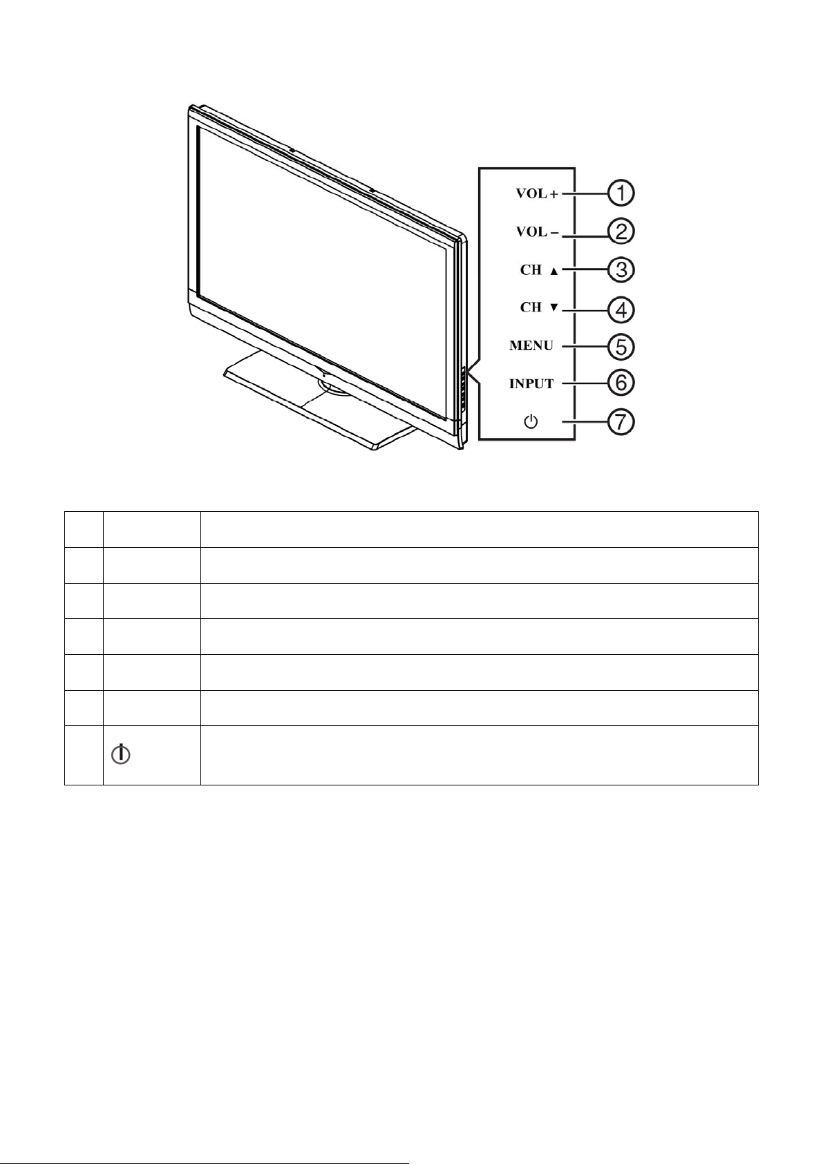
2.3 Front Panel Control Knobs
1. VOL + VOL +: Press to increase the sound volume level.
2. VOL - VOL -: Press to decrease the sound volume level.
3. CH Ÿ CH Ÿ: Press to select the next higher Programme number.
4. CH ź CH ź: Press to select the next lower Programme number.
5. MENU Menu key: Press to open or exit the OSD (on-screen display) menu.
6. INPUT Input key: Press to select the input source.
7.
POWER
Power key: Press to turn on / off (standby) the TV set. (Press to turn on TV after the
power on status, LED had changed to the Blue colour and stopped flashing.)
12
Page 13
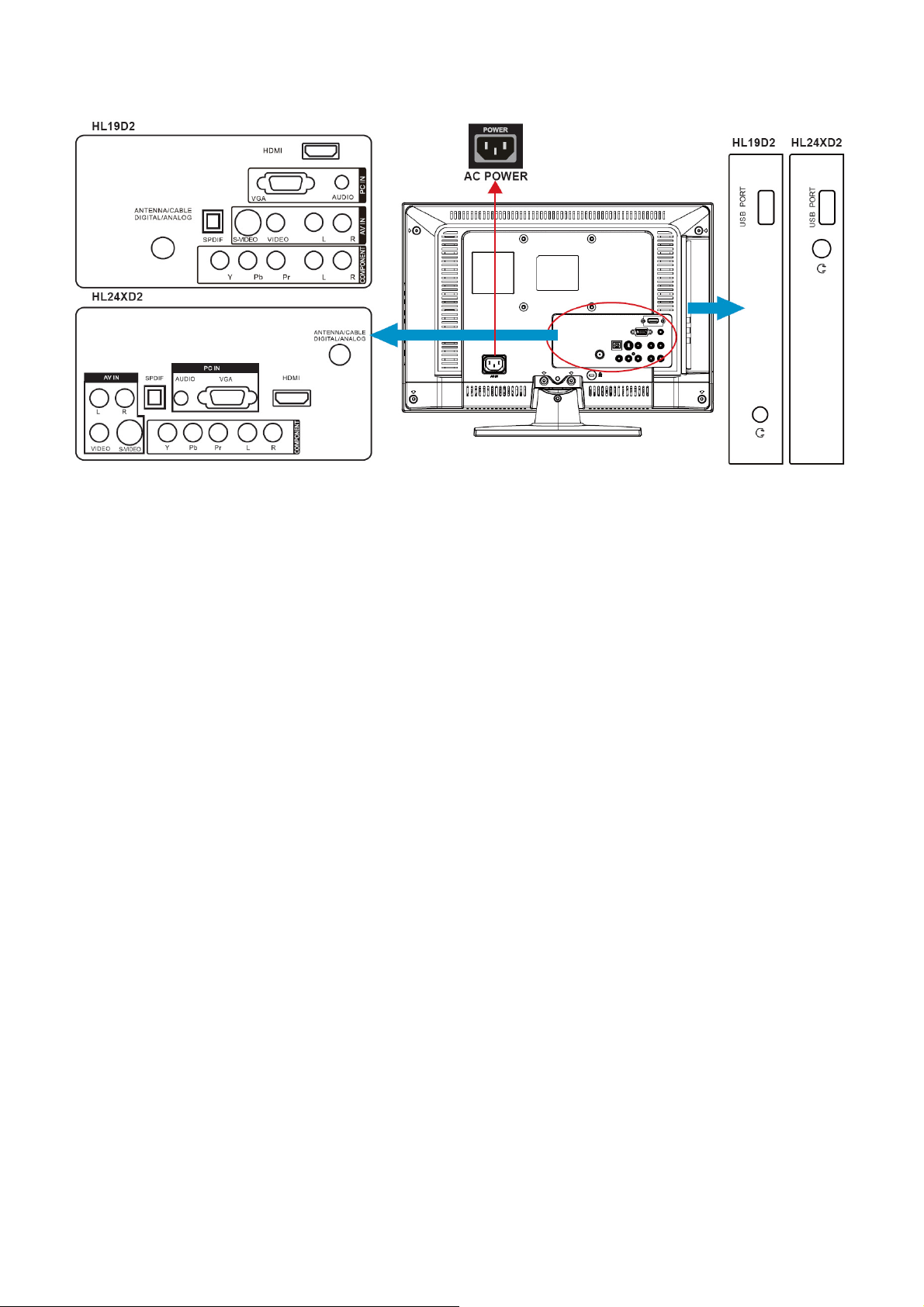
2.4 How to Connect
1. HDMI – Connect the primary source for digital video such as a DVD multimedia player or set top box through this
all digital connector.
2. PC IN – Connect the video and audio cables from a computer here.
3. AV IN (AV/S-VIDEO) – Connect the input source for composite video devices, such as a VCR or video game. Use
the white and red connectors to connect the external audio from the same source. The signal being carried by the
S-Video cable and connector, if connected, will take priority over the Video RCA connector (yellow connector).
444 COMPONENT (Y/Pb/Pr with Audio L/R) – Connect the primary source for component video devices such as a
DVD Player or set top box here. Use red for Pr, blue for Pb, green for Y, red for right audio (R) and white for left
audio (L) inputs.
5. ANTENNA/CABLE DIGITAL/ANALOG – Connect to an antenna or digital cable (outof- the-wall, not from Cable
Box) for Digital TV.
6. SPDIF (Optical Digital Audio Out) – When a digital audio signal is associated with the input selected for viewing,
the digital audio will be available on this SPDIF connection to your home theater system.
7. USB PORT – Insert USB storage device to the USB port to view photos or listen to music.
8. Earphone Output – Connect to the headphones. When the headphone is inserted to the plug, all the speakers
will be muted.
Once your equipment is connected, use the following procedure to view the input signal:
Press the Source button on the remote control to select the relevant source to view. (ex: Press Comp
button to select “Component” if you have connected a video recorder to Component socket.)
13
Page 14
3. Input/Output Specification
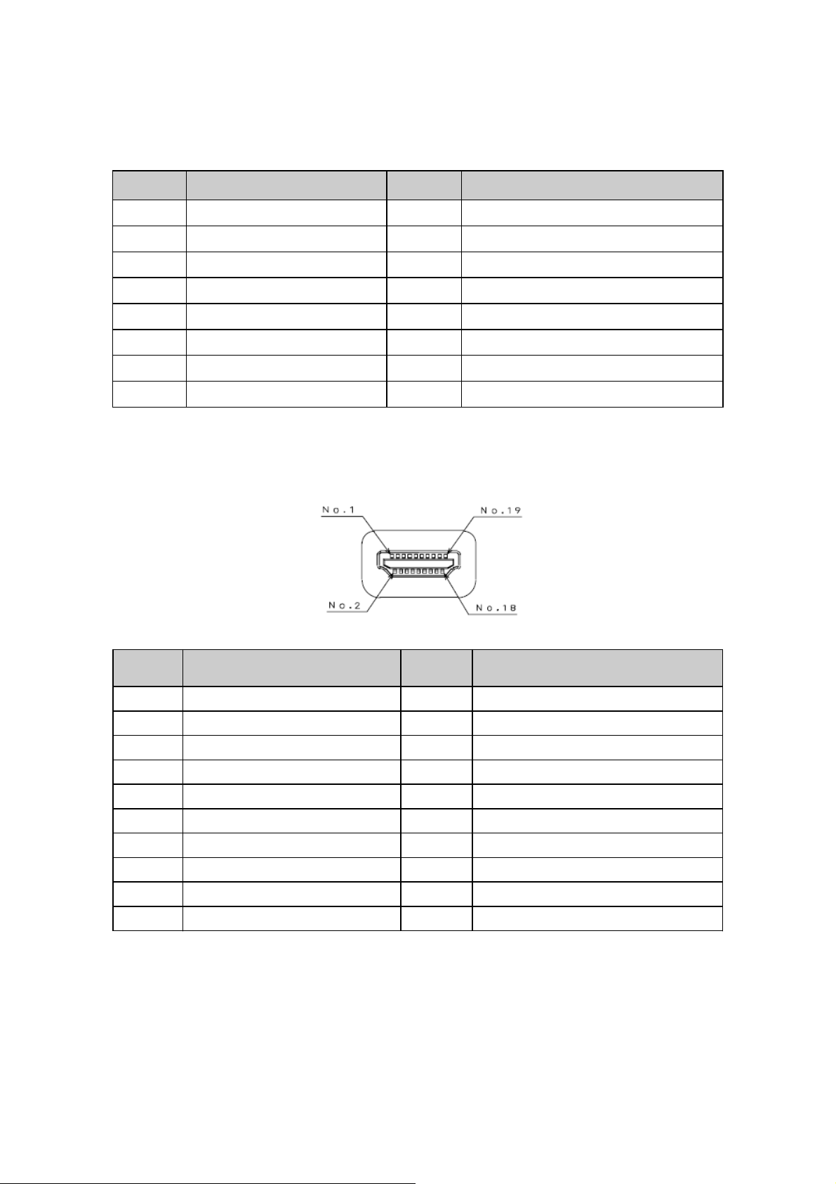
3.1 Input Signal Connector
D-SUB
Pin No. Description Pin No. Description
1 Red Video 9 No Pin
2 Green Video 10 Sync GNDʳ
3 Blue Video 11 SDA(Remote Control)
4 SCL(Remote Control) 12 Serial Data for DDC
5 Ground 13 H. Sync
6 Red Ground 14 V. Sy n c
7 Green Ground 15 Serial Clock for DDC
8 Blue Ground
HDMI
Pin No. Description Pin No. Description
1 TMDS Data2+ 11 TMDS Clock Shield
2 TMDS Data2 shield 12 TMDS Clock-
3 TDMS Data2- 13 CEC
4 TMDS Data1+ 14 NC
5 TMDS Data1 shield 15 SCL
6 TMDS Data1- 16 SDA
7 TMDS Data0+ 17 DDC/CEC Ground
8 TMDS Data0 shield 18 +5V Power
9 TMDS Data0- 19 Hot Plug Detect
10 TMDS Clock+
14
Page 15
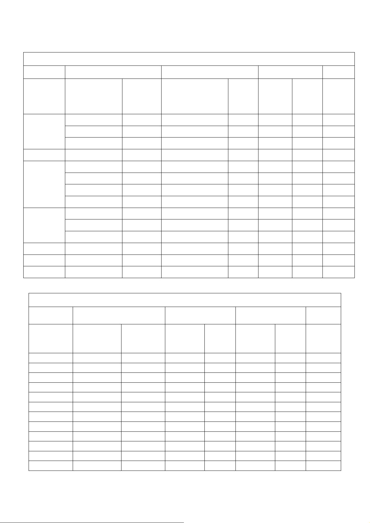
3.5 Input Signal Timing
Analog RGB:
VESA MODES
Horizontal Vertical
Mode Resolution Total
640x480@60Hz 800 x 525 31.469 N 59.940 N 25.175
VGA
DOS 720x400@70Hz 900 x 449 31.469 N 70.087 P 28.322
SVGA
XGA
CVT-0.92M9 1280x720@60Hz 1664 x 748 44.722 N 59.855 P 74.500
WXGA 1280x768@60Hz 1440 x 790 47.396 P 59.995 N 68.250
640x480@72Hz 832 x 520 37.861 N 72.809 N 31.500
640x480@75Hz 840 x 500 37.500 N 75 N 31.500
800x600@56Hz 1024 x 625 35.156 P 56.250 P 36.000
800x600@60Hz 1056 x 628 37.879 P 60.317 P 40.000
800x600@72Hz 1040 x 666 48.077 P 72.188 P 50.000
800x600@75Hz 1056 x 625 46.875 P 75 P 49.500
1024x768@60Hz 1344 x 806 48.363 N 60.004 N 65.000
1024x768@70Hz 1328 x 806 56.476 N 70.069 N 75.000
1024x768@75Hz 1312 x 800 60.023 P 75.029 P 78.750
Nominal Frequency
(KHz)
Sync
Polarity
Nominal
Freq.
(Hz)
Sync
Polarity
Nominal
Pixel
Clock
(MHz)
WXGA 1360x768@60Hz 1720 x 795 75.000 P 60.020 P 162.000
HDMI
VESA MODES
Horizontal Vertical
Nominal
Mode Resolution Total
DOS 720 x 400 900 x 449 31.469 N 70.087 P 28.322
VGA 640 x 480 800 x 525 31.469 N 59.940 N 25.175
SVGA 800 x 600 1056 x 628 37.879 P 60.317 P 40
XGA 1024 x 768 1344 x 806 48.363 N 60.004 N 65
WXGA 1280 x 768 1664 x 798 47.396 P 59.995 N 68.25
CVT-0.92M9 1280 x 720 1664 x 748 44.772 N 59.855 P 74.5
WXGA 1360x768@60Hz 1720 x 795 75.000 P 60.020 P 162.000
1080P 1920 x 1080P 2200 x 1125 67.5 60, 148.5
720P 1280 x 720P 1650 x 750 45.00 60, 74.25
1080i 1920 x 1080i 2200 x 1125 33.75 60, 74.25
480P 720 x 480P 858 x 525 31.50 60, 27.03
480i 720 x 480i 1716 x 525 15.75 60, 13.51
Frequency
(KHz)
Sync
Polarity
Nominal
Freq.
(Hz)
Sync
Polarity
Nominal
Pixel
Clock
(MHz)
15
Page 16
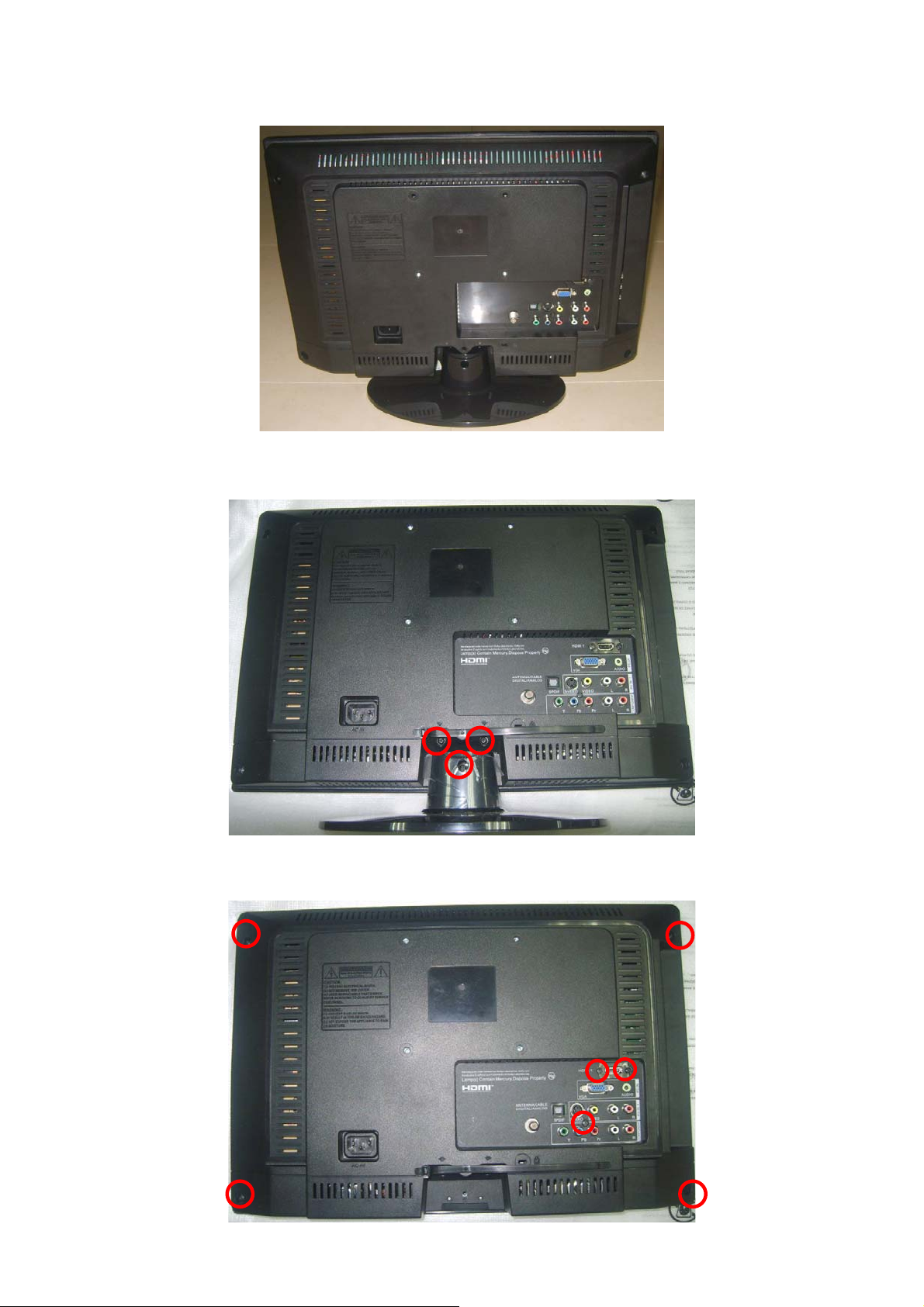
4. Mechanical Instructions
Rear view
Step1. Remove the STAND ASS’Y.
Unscrew the 3 screws.
Step2. Remove the REAR COVER.
Unscrew the 7 screws.
16
Page 17

Step 3. Disconnect the WIRE HARNESS.
Disconnect the 7 WIRE HARNESS.
Step 4. Remove the MAIN, POWER BOARD and BEZEL.
Unscrew the 9 screw for boards and 2 screws for BEZEL.
17
Page 18

18
Page 19

Step 5. Remove the MAIN FRAME and PANEL.
Unscrew the 4 screws.
19
Page 20

5. Repair Flow Chart
p
1. No power
No power (LED “Off”)
Check the AC input and
the
ower is “On”?
Yes
Power board output=5V?
Yes
Check the IR board and LED
Replace the IR board
No
Replace the main board
No
Power “On”
No
Replace the power board
20
Page 21

2. Can’t start
Can’t start (LED Red)
Power board output᧹12V?
Yes
No
Replace the power board
Yes
Check the power key is under control?
No
Check the IR receiver is normal?
No
Replace the main board
No
Replace the Power board
Replace the key board
Yes
Replace the IR board
21
Page 22

3. No display
No display (LED Blue)
Check TV is under control and power
on/off by remote control and power key?
Yes
Check the LVDS cable
Yes
Yes
Check the backlight is
“On”?
No
Reinsert or replace the
LVDS cable
No
No
Check the B/L
signal is available?
Yes
Replace the main board
No
Replace main board
Panel Vcc = 5 V?
Yes
Replace the Panel
No
Replace the main board
Power board output᧹12V?
Yes
Replace the Panel
Replace the power board
No
22
Page 23

4. Sound problem
No sound or sound abnormal
Check the audio source connection
and the TV system are correct˛
No
Yes
Check the TV is muted, adjust the
volume or enter the menu to reset?
No
Check the cable between the
speakers and main board is ok?
Yes
Check the speaker resistance value is in spec
(Remark: The value is marked on the speaker)?
Yes
Reinsert the audio cable or
change the TV system
Replace the main board
No
Replace the cable
No
Replace the speaker
23
Page 24

5. Remote Control malfunction
prop
OSD is unstable or can’t work normally
Key board connected properly?
Yes
Buttons are ok?
Yes
Key board is ok?
Yes
Replace the main board
6. OSD is unstable or can’t work normally
No
Reconnect the key board
No
Replace the button function
No
Replace the key board
Remote Control malfunction
Check the remote control battery is
not
erlyplaced or no power?
No
Use the other remote controls
No
Whether the IR board is
abnormal?
No
Yes
Replace the battery
Yes
Replace the remote control
Yes
Replace the IR board
Replace the main board
24
Page 25

6. PCB Layout
6.1 Main Board
715G3239M01002005F
25
Page 26

26
Page 27

27
Page 28

6.2 Power Board
715G2783 3 7
28
Page 29

29
Page 30

6.3 Key Board
715G3303 1
6.4 IR Board
715G3963R01000004S
30
Page 31

7. Adjustment
It’s no need to adjust the white balance for this model, do ADC only.
Step1: Turn on the TV, press “Menu”, then press number key 1 Æ 9 Æ 9 Æ 9 and “ENTER”, it will achieve the factory
mode. Take the following picture for example:
Step2: Change TV, press the “Current Source” to Component mode and change signal to 1080i mode, press the
“Auto Color”;
Step3: Change TV, press the “Current Source” to PC mode and change signal to PC TIMING 137(1024X768);
Pattern 147 (16 Grays), press the “Auto Color”.
31
Page 32

TU201
ENV56U03D8F
TVM_PWR_ON1
VCC1_1V
VCC3_3
VCC1_8_DDR
VCC1_8
VCC3_3_STB
VCCA1_8_STB
5VT
26"
ONLY
U707
U601
TPA3113D2
G9084
U705
AP1084D18L
U703
G1084-T43Uf
VCC3_3
for 26"
P24V
Inverter
5V,12VPOWER-ON
POWER
BOARD
19-22
KEYPAD
Q701
AO4449
ONLY
U704
P12V
G5627F11U
U701
G5627F11U
U708
G1084-33T63Uf
Q704
AO4449
U706
G5628ADJT1U
BL_ON_OFF
BL_BR_CTRL
+5VSB
POWER
BOARD
SPEAKER
EAR PHONE
32
IR
EARPHONE AMP
LCD PANEL
LVDS
DDRII
GPIO
NT5TU32M16BG-25D
FLASH ROM
M25P32-VMF6TP
USB 1.0
EJTAG
M24C64
S/PDIF
SPDIF
Audio Amplifier
TPA3113D2
Analog R/L
TPA6113A2DR
Analog R/L
Digital
Tuner
VIF
ENV56U03D8F
CVBS
CVBS1
8. Block Diagram
ZR39775
TMDS
HDMI-1
TMDS
SiI9185ACTU
TMDS
HDMI-2
CVBS1/S-Video AUDIO-R\L
reserve reserve
CVBS2 AUDIO-R\L
YPbPr AUDIO-R\L
VGA AUDIO-R\L
Hsync, Vsync
YPbPr
Y/C
CVBS
RGB
SN74LVC1G17DBVR
I2C
M24C02
YPbPr
S-VIDEO
CVBS2
VGA
Page 33

For ZR39775 Digital 1.8V
DDR II
BLUE: Load
Black: LDO
U601
TPA3113D2
RED: P MOS
Inverter
GREEN: DC/DC
SPI Flash
TU201
ENV56U03D8F
5VT
152mA
U401 ZR39775
CORE_VDD18STDBY
For ZR39775 Core
U40 4 M 25L 32
VCC3_3
VCC1_1V
0.56A
1.36A
EEPR OM
U40 2
M24C64-WMN6P
VCC1_8
For ZR39775 Digital 3.3V
U705
AP1084T43UF
VCC1_8_DDR
?A
For ZR39775 AVDD, SIF,
IF, PLL, DAC, LDI
33
U703
AP1084T43UF
U701
U707
PANEL
?A
D12V
G9084
U401 ZR39775
IOVDD_STBY
?A
VCC3_3_STB
VGA EDID
U706 G5628
U201 M24C02
PANEL
EEPRO M
?A
VCC5D
Q704
AO4449
U704
USB
G5627F11U
G5627F11U
P24V
Q701
P12V
AO4449
?A
+5VSB
?A
POWER
BOARD
BL_ON_OFF
BL_BR_CTRL
Page 34

Panel
LVDS Cable
30 Pin
CN409
U401
Scaler IC
ZR39775HGCF
Tuner
TU202
34
12 Pin
CN701
CN604
4 Pin
9 Pin
CN407
Speaker R/L
5Pin
CN201
11 Pin
To Panel
9. Wiring Diagram
CN902
2 Pin
CN802
IR Board
Power Board
2 Pin
CN803
Key
Board
4 Pin
CN01
Page 35

Demodul ator
IF_AINN
IF_AINP
SIF_AI NN
SIF_AI NP
U401P
SIF_N
SIF_P
AF2
AE2
AF4
AE4
AD3
IF_R BIAS
DEMOD_CLKO
IF_RBIAS
IF_VINBIAS
IF_VCM
IF_VREFN
IF_VREFP
AF1
AE1
AC7
AD8
AD2
AD1
IF_VREFP
IF_VREFN
IF_VCM
IFE_VBIAS
IF_AGC
RF_AGC
DMOD_RST_N
MPEG _FA IL
PARAM0
SA_DATA
IF_DVAL_GPIO
ZR39775H GCF-B
AF7
AF8
AE7
AA5
AC8
AC6
PARAM0
RF_AGC
C204 10N 50V
C203
10N 50V
R202
NC/47 OHM 1/10W
C202 NC/0.1UF16V
Place parts very close to U401
SIF
〄ǂ
DIF
IF_AINN
C277 1nF 50V
ǂɇ
L201,L203 change to 47ohm
C209 100P 50V
C215 100N16V
C214 100N16V
C212 100N16V
C211 100N 16V
R204
3.9K1/10W
IF_AINP
C278 1nF 50V
C217
C210
NC
C213
82pF50V
L202
0.15uH
Change 5%
L201
47R 1/8W
L203
47R 1/8W
L205
0.082uH
L204
0.082uH
C216 100P 50V
IF_AN
IF_AP
R208 2K 1/10W
C218
100N16V
R206 4K7 1/10W 5%
R205 0R05 1/10W
R207 NC/20K OH M 1/10W
IF_AGC
VCC3_3
DEMOD_RSTN8
NC
ENV56U03D8F
ET-29DHRV
Panasonic suggest for
Place parts very close to
U401
TU_C VB S 4
FB205
NC/30 OHM
1 2
V-OUT
ZD204
NC
1 2
IF_AGC
ZD203
NC
1 2
35
C201
470uF 16V
+
ǂǂ㬐ǂ
C206
1.5nF 50V
C205
560pF 50V
5VT
I2C1_SD A 6,7
I2C1_SC L 6,7
0.1uF,1nF-->0402
R238
2K2 1/10W 5%
R237
2K2 1/10W 5%
R201 22R 1/10W 5%
R203 22R 1/10W 5%
ZD202
C208
22pF 50V
C207
22pF 50V
VPORT0603100KV05
1 2
1 2
ZD201
TU_S CL
TU_S DA
VPORT0603100KV05
5VT
5VT
FB202
FB201
600 OHM
1 2
1 2
C220
2N2 50V
C219
0.1uF 50V
C240 2N2 50V
C235 NC
TU_SC L
V-OUT
SIF
B+
BT Monitor
3
2
1
5
11
13
6
BB
NC
NC
NC8NC9NC10NC
SCL
AGC
BT Monitor
TU201
V-OUT
5VT
FB203
NC/600 OHM
NC
1 2
C222
NC/0. 001uF
C224
NC
C223
C221
TU_SD A
15
14
NC
SDA
NC
NC
C268
1uF 16V
C270
NC
C271
NC
C241
NC
IF_AN
IF_AGC
IF_AP
IF_Monitor
17
25
20
16
21
+B
TH122TH223TH324TH4
IF AGC
IFD- out119IFD- out2
IF Monitor
NC / TUNER
94GNTAT MA8MA
TU202
TUN ER
ENV56U03D8F
ET-29DHRV
TU_S CL
TU_S DA
IF_AP
BT Monitor
5
6
NC
BT Monitor
91412
10115
10
9
SCL
SDA
6131
IF_AN
IF_AGC
14
12
11
IF AGC
IFD-out113IFD-out2
TH1
IF Monitor
15
TH2
16
TH3
17
TH4
18
3
2
5V:
+B(DC/DC)=15mA(MAX)
+B(Tuner)=150mA(MAX)
B+
1
2
3
+B
NC
RF-AGC Monitor
10. Schematic Diagram
10.1 Main Board
715G3239M01002005F
03) Tuner
Page 36

Video In I/F
SVIDEO0YU3SVIDEO0C
U401F
SVIDEO1YU4SVIDEO1C
V3
V4
SVIDEO2YU5SVIDEO2C
V5
AA3
CVBS0
CVBS1
CVBS2
CVBS3
AB3
AB4
AA4
VIN_R1U2VIN_G1U1VIN_B1
V1
VIN_R2W2VIN_G2W1VIN_B2
SOY_I N0
V2
Y1
Y2
SOY_I N1
SOG_IN0
VGA_R0T2VGA_G0T1VGA_B0
T4
T3
AFE_HS_I NR5AFE_VS_IN
VGA_SCL_GPIO_P28
VGA_SDA_GPIO_P29
T5
AE9
AB11
AA1
VCOM
VREFP
VREFN
AA2
RSETL4REFNODE_GND_CVBSW3REFNODE_GND_RL5REFNODE_GND_GK5REFNODE_GND_BM5REFNODE_GND_Ch
AB1
ZR39775HGC F-B
N5
C228 0.22uF 16V
S1_Y
C229 0.22uF 16V
S1_C
C246 10N 50V
C243 0.22uF 25V
C244 0.22uF 25V
C245 0.22uF 25V
C231
NC/220pF
C230
NC/ 220pF
R216 75R 1/10W 1%
AV1_CVBS
C234 0.22uF 16V
R215 75R 1/10W 1%
R219 75R 1/10W 1%
R220 75R 1/10W 1%
C239 NC/ 0.22uF16V
C242
C237
NC/ 220pF
NC/ 220pF
AV2_CVBS
R262 75R 1/10W 1%
R226 75R 1/10W 1%
C232 NC/ 0.22uF10V
YPBPR _PB
YPBPR _PR
YPBPR _Y
C233
NC/ 220pF
R235 1K 1/10W 5%
R234 75R 1/10W 1%
R233 75R 1/10W 1%
R232 75R 1/10W 1%
C249
NC
C248
NC
C247
NC
C254 0.22uF 25V
C255 0.22uF 25V
VGA_G
VGA_R
VGA_R5
C256 0.22uF 25V
VGA_B
VGA_G5
C257 10N 50V
RGB_HSYNC_F
RGB_VSYNC_F
RGB_HSYNC_F5
RGB_VSYNC_F5
C274
NC
C273
NC
C272
NC
VGA_B5
C262 4.7uF 10V
C264
R252
62KOHM + -1% 1/10W
0.47uF 16V
36
YPBPR _Y
YPBPR _PB
TU_CVBS3
YPBPR _PR
S1_Y
S1_C
Length tolerance within + - 100 mil
75R 1/10W 1%
R246
AV2_AUDIO_L 12
R218
75R 1/10W 1%
R217
75R 1/10W 1%
C276
47pF 50V
ZD206
VPORT0603100KV05
1 2
C275
47pF 50V
ZD205
VPORT0603100KV05
1 2
1 2FB209 30 OHM
1 2FB210 30 OHM
5
4
2
8
AV1_CVBS
R230
75R 1/10W 1%
2
3
FB211
30 OHM
1 2
6
7
1 3
GND
I/O34I/O4
U206
CN20 1
JACK
I/O11I/O2
AZ2025-04S.R 7G
5
21436
CN202
1 2FB214 30 OHM
1 2FB215 30 OHM
PB
75R 1/10W 1%
R248
R245
75R 1/10W 1%
1 2FB216 30 OHM
PR
5
JACK
FB212
NCCN204
AV2_CVBS
R223
NC
NC/30 OHM
1 2
ZD208
NC
6
7
8
9
AV2_AUDIO_R 12
ZD210
NC
1 2
1 2
ZD209
NC
1 2
1
2
3
4
5
04) AV Input
S_DET6
Page 37

VGA_EDID _WP 8
VGA_R 4
VGA_B 4
VGA_G 4
VGA_B
VGA_G
VGA_R
R257
75R 1/10W 1%
R256
75R 1/10W 1%
R255
75R 1/10W 1%
2
1
3
I/O1
I/O2
GND
I/O34VDD5I/O4
U204
AZC099-04S. R7G
C265 0.1uF 50V
6
VCC5D
1 2FB218 30 OHM
1 2FB217 30 OHM
1 2FB219 30 OHM
C250
Length tolerance within + - 100 mil
10pF 50V
VGA_EDID _WP
R276 33 OHM 1/1 0W
R224
1K 1/10W 5%
R222
R221
4.7K 1/10W
4.7K 1/10W
R231
10K 1/10W
VGA_SDA 4, 11
VGA_SCL 4,11
VGA_SDA
VGA_SCL
ZD214
VCC5_0_VGA
VPORT0603100KV05
1 2
1716
R254 1K 1/ 10W 5%
R253 33 OHM 1/10W
UART0_RX7,11
UART0_TX7,11
C251
C252
162738495
1112131415
10
10pF 50V
10pF 50V
2
ZD207
BAT54C
1
VCC5_0_VGA +5VSB
CN203
DB15
18 19
R259
10K 1/10W
1
3
2
I/O1
I/O2
GND
I/O34VDD5I/O4
U205
AZC099-04S. R7G
6
C266 0.1uF 50V
VCC5_ED ID
R260
2K2 1/10W 5%
R258
2K2 1/10W 5%
RGB_HSYNC_F 4
R244
33 OHM 1/10W
VCC5_EDID
R227 22R 1/1 0W 5%
U201
8
7
VCC
A01A12A23GND
R228 22R 1/1 0W 5%
5
6
WP
SCL
SDA
AT24C02BN-SH-T
4
RGB_VSYNC_F 4
RGB_VSY NC_F
C263
R251
33 OHM 1/10W
NC/ 330pF
VGA_VSYN C 7,8
VGA_VSYN C
37
3
C238
0.22uF 25V
VGA_HSY NC 8
VGA_HSY NC
C261
NC/ 47pF
05) VGA Inputs
SN7 4LV C1G17 DBVR
RGB_HSYNC
RGB_VSY NC
VGA_SCL
VGA_SDA
U202
2 453
VCC3_3
C260 0.1uF 50V
R243
100R 1/10W 5%
RGB_HSYNC RGB_HSYNC_F
R242
5.1K 1/10W
R239
2K2 1/10W 5%
U203
SN74LVC1G17DBVR
2 453
VCC3_3
R250
100R 1/10W 5%
RGB_VSY NC
R249
5.1K 1/10W
R247
2K2 1/10W 5%
Page 38

U401G
Run As 100 Ohm
Differential
Pairs
3V3_STB
HDMI0_5V
+5VSB
HDMI0_5V
HDMI0 I/ F
HDMI0_D2PB8HDMI0_D2NA8HDMI0_D1PC8HDMI0_D1NC9HDMI0_D0PA9HDMI0_D0NB9HDMI0_CLKP
HDMI_D2P
HDMI_D2N
HDMI_D1P
VCC3_3_STB
3V3_STB
ZD501
NC/BAT54C
2
1
R542
HDMI0_5V
D501
HDMI0_D0N
HDMI0_D0P
9
7
CN501
TMDSD0+
GPIO_P18
GPIO_P14
HDMI1_D0N
HDMI1_D0P
AVCC33
HDMI1_D1N
HDMI1_D1P
HDMI 1_D2N
HDMI 1_D2P
AVCC18
DDC1_SDA
DDC1_SCL
HDMI 1_5V
AVCC33
AVCC18
10
NC9NC
Line-11Line-22VDD3Line-34Line-4
+5VSB
HDMI0_D1N
HDMI0_D1P
10
NC9NC
Line-11Line-22VDD3Line-34Line-4
+5VSB
HDMI0_CLKN
HDMI0_CLKP
GPIO_P12
C7
R526 NC/0 OHM 1/10W
R532 10K 1/10W
R531 10K 1/10W
R530 10K 1/10W
VCC3_3_STB
HDMI1_5V
AVCC33
HDMI1_CLKP
39
40
AGND
R1X0-
41
R1X0+
42
AVCC33
43
R1X1-
44
R1X1+
45
AGND
46
R1X2-
47
R1X2+
48
AVCC18
49
DSDA1
50
DSCL1
51
RPWR1
52
CEC_D
53
CEC_A
54
AVCC33
55
HPD2
56
AVCC18
57
R2XC-
58
R2XC+
59
AGND
60
R2X0-61R2X0+62AVCC3363R2X1-64R2X1+65AGND66R2X2-67R2X2+68AVCC1869DSDA270DSCL271RPWR272DVDD1873DGND74TEST75HPDIN76TSDA77TSCL78TPWR/I2CADDR79AGND
8
7
NC6NC
GND
AZ1045-04QU.R DG
5
C524
0.1uF 50V
HDMI0_D2N
HDMI0_D2P
7
8
NC6NC
GND
AZ1045-04QU. RDG
5
C528
0.1uF 50V
HDMI0_D0P
HDMI0_D0N
HDMI2 I/ F
HDMI2_D2PD1HDMI2_D2ND2HDMI2_D1PC1HDMI2_D1NC2HDMI2_D0PB1HDMI2_D0NB2HDMI2_CLKPA1HDMI2_CLKNA2HDMI2_SCLB3HDMI2_SDAA3HDMI2_HPDD4HDMI2_5VSENSE
DGND
I/O2
I/O34VDD5I/O4
U401D
DDC0_SDA
DDC0_SCL
HDMI0_5V
DVDD18
33
30
31
32
DSCL0
RPWR0
DVDD18
NC/SiI 9185ACTU
AVCC18
DDC0_SCL
1
2
I/O1
GND
AZC099-04S. R7G
6
+5VSB
DDC0_SDA
HDMI0_D0N
HDMI0_D0P
HDMI0_D1N
HDMI0_D1P
HDMI0_D2N
HDMI0_D2P
AVCC33
AVCC18
23
29
21
24
27
22
26
28
R0X0-
R0X1-
R0X2-
R0X0+
R0X1+25AGND
R0X2+
DSDA0
AVCC18
DVDD18
C525
0.1uF 50V
AGND
AVCC33
20
R0XC+
19
R0XC-
18
AVCC18
17
HPD0
16
LSCL/PSEL1
15
LSDA/PSEL0
14
RESET#
13
ExtSWING
12
TXC-
11
TXC+
10
AGND
9
TX0-
8
TX0+
7
AVCC18
6
TX1-
5
TX1+
4
AGND
3
TX2-
2
TX2+
1
80
TSDA
TSCL
HPDIN
R528 NC/0R05 1/10W
R529 NC/0R05 1/10W
R541 NC/0R05 1/10W
R540 NC/0R05 1/10W
HDMI_SCL
HDMI_SDA
HDMI_HPD
HDMI_5V
HDMI_CEC
DDC1_SCLDDC1_SDA
1
3
2
I/O1
I/O2
GND
I/O34VDD5I/O4
U507
NC/AZC099-04S
6
C527
0.1uF 50V
+5VSB
HDMI1_HPD
ZR39775HGCF-B
R527 4K7 1/10W 5%
NC/10K 1/10W
R514
HDMI1_HPD
HDMI1_CLKN
AVCC18
37
36
35
34
38
HPD1
R1XC-
R1XC+
AVCC18
I2CSEL/INT
U501
AVCC33
HDMI_CEC
3
U504
HDMI0_HPD
GPIO_P17
GPIO_P15
GPIO_P16
HDMI1 I/ F
HDMI1_D2PB4HDMI1_D2NA4HDMI1_D1PC4HDMI1_D1NC5HDMI1_D0PA5HDMI1_D0NB5HDMI1_CLKPB6HDMI1_CLKNA6HDMI1_SCLB7HDMI1_SDAA7HDMI1_HPDD6HDMI1_5VSENSE
HDMI0_CLKN
HDMI0_SCL
HDMI0_SDA
HDMI0_HPDD9HDMI0_5VSENSED7HDMI_ATESTD3HDMI_REXT
HDMI0_CEC
D8
B10
A10
B11
A11
HDMI_CEC_SW
HDMI_SCL
HDMI_SDA
HDMI_D1N
HDMI_D0P
HDMI_D0N
HDMI_CLKP
HDMI_CLKN
R517
R516
HDMI_CEC_SW
R546
27K 1/10W
Q501
NC/2SK3018
R545
NC
3
HDMI_CEC
HDMI_HPD
R544
Q502
2N7002 SOT-23
4K7 1/10W 5%
Q503
2N7002 SOT-23
R543
1K 1/10W 5%
R559
HDMI0_HPD
DDC0_SCL
BAT54C
4K7 1/10W 5%
R505
4K7 1/10W 5%
R504
R506 0R05 1/10W
HDMI0_D2N
HDMI0_D1P
HDMI0_D1N
HDMI0_D2P
HDMI0_CLKN
HDMI0_CLKP
15
6
3
12
10
4
1
TMDSC -
TMDSC+
TMDSD0-
TMDSD1-
TMDSD2-
TMDSD1+
TMDSD2+
ZR39775HGC F-B
C3
R525
10KOHM +-5% 1/10W
R520 10K 1/10W 5%
R521 390R 1/10W 1%
R519 0R05 1/10W
R515 1K 1/10W 5%
HDMI_5V
HDMI_HPD
VCC3_3_HDMI
NC/1. 8K OHM 1/10W 5%
C531
NC/47pF 50V
NC/1. 8K OHM 1/10W 5%
DDC0_SDA
R508 0R05 1/10W
16
SCL
EMI add
C530
NC/47pF 50V
HDMI_D1N
HDMI_5V
HDMI_SDA
HDMI_SCL
876
123
R557 0R05OHM1/16W
R556 0R05OHM1/16W
R558 0R05OHM1/16W
RP501
HDMI0_5V
DDC0_SDA
DDC0_SCL
HDMI0_D1N
NC/4K7 1/ 10W 5%
10K 1/10W
HDMI_CEC
HDMI0_HPD
HDMI0_5V
C501
0.1uF 50V
FB507
120 OHM
R501 0R05 1/10W
R512 NC/0R05 1/10W
1 2
14
5
2
8
18
19
13
NC
SDA
HPD
CEC
VCC5
DSHLD1
DSHLD0
U401O
Zoran Gavin change
HDMI_CLKP
HDMI_CLKN
HDMI_D2N
HDMI_D2P
HDMI_D0N
HDMI_D0P
HDMI_D1P
5
876
5
4
123
4
for only rear HDMI
RP502
0OHM1/16W
0OHM1/16W
HDMI0_CLKP
HDMI0_D2N
HDMI0_D1P
HDMI0_D0P
HDMI0_D0N
HDMI0_D2P
HDMI0_CLKN
U502
U503
11
21
26
17
SHLD122SHLD223SHLD324SHLD425SHLD5
CSHLD0
DSHLD2
DDC_GND
SHLD_GND 120SHLD_GND 2
HDMI
GPIO_P20
ZR39775HGCF-B
E6
R551 , R536 EMI issue
C509
NC/0. 1uF 50V
C536
0.1uF 50V
R550 0R05 1/10W
R534 10K 1/10W
R535 NC / 10K 1/10W 5%
R533 10K 1/10W
300 OHM
R537 10K 1/10W
1 2
R551
VCC3_3_STB
S_DET
VCC3_3
S_DET4
HDMI_RSTn 8
I2C1_SCL 3,7
I2C1_SDA 3,7
HDMI 0_CLKP
HDMI 0_CLKN
AVCC18
HDMI0_HPD
HDMI_RST
EXTSWIN G
HDMI_CLKN
HDMI _CLKP
HDMI_D0N
HDMI _D0P
AVCC18
HDMI_D1N
HDMI _D1P
HDMI_D2N
HDMI _D2P
R511 NC/0R05 1/10W
R502 NC/0R05 1/10W
R507 NC/0R05 1/10W
I2C2_SCL_HDMI
I2C2_SDA_HDMI
C533
NC/100pF 50V
C532
NC/100pF 50V
CN502
20
AVCC33
C508
Zoran Gavin change
AVCC33
AVCC18
R539 NC/820R 1/10W 1%
R513 NC/10K 1/10W
Zoran
Gavin
10
Line-11Line-22VDD3Line-34Line-4
U505
HDMI1_D1P
HDMI1_D1N
+5VSB
HDMI1_D2N
HDMI1_D1P
HDMI1_D1N
HDMI1_D2P
2
5
1
4
3
6
D2-
D2+
D1+
D2 Shield
D1 Shield
SHELL1
SHELL3
22
NC/0. 1uF 50V
C507
NC/0. 1uF 50V
C506
NC/0. 1uF 50V
C505
NC/10uF 16V
C504
NC/10uF 16V
FB501
NC/120 OHM
1 2
C503
0.1uF 50V
VCC3_3_STB
reserve
8
7
NC6NC
NC9NC
GND
NC/AZ 1045-04QU
5
C526
NC/0. 1uF 50V
+5VSB
HDMI1_D2P
HDMI1_D2N
DDC1_SCL
DDC1_SDA
R523
NC/4K7 1/ 10W 5%
R522
NC/4K7 1/ 10W 5%
HDMI_CEC
HDMI1_5V
HDMI1_CLKP
HDMI1_D0N
HDMI1_D0P
HDMI1_CLKN
R524 NC/0R05 1/10W
R509 NC/0R05 1/10W
R510 NC/0R05 1/10W
10
8
12
7
9
D1-
D0+
D0 Shield
18
14
17
13
11
15
16
NC
D0-
CK-
CK+
GND
CK Shield
DDC CLK
DDC DATA
CE Remote
SHELL4
23
C523
NC/0.1uF 50V
C522
NC/0. 1uF 50V
C521
NC/0.1uF 50V
C520
NC/0. 1uF 50V
C519
NC/0. 1uF 50V
C518
NC/0. 1uF 50V
AVCC18
C517
NC/0. 1uF 50V
C516
NC/10uF 16V
C515
NC/10uF 16V
FB503
NC/120 OHM
1 2
C514
NC/0. 1uF 50V
VCCA1_8_STB
C513
NC/0. 1uF 50V
DVDD18
C510
NC/0. 1uF 50V
C512
NC/10uF 16V
FB502
NC/120 OHM
1 2
C511
NC/0.1uF 50V
VCCA1_8_STB
8
7
10
NC6NC
NC9NC
GND
Line-11Line-22VDD3Line-34Line-4
U506
NC/AZ 1045-04QU
5
C529
NC/0.1uF 50V
+5VSB
HDMI1_CLK N
HDMI1_CLK P
HDMI1_D0P
HDMI1_D0N
HDMI1_HPD
R503 NC/0R05 1/10W
C502
NC/0. 1uF 50V
19
+5V
HP DET
SHELL2
NC/HDMI
21
38
06) HDMI Input
Page 39

I2C0_SDA
I2C0_SCL
I2C0_EEPROM_WP8
I2C0_EEPROM_WP
R402
10K 1/10W
R415 22R 1/ 10W 5%
R413 22R 1/ 10W 5%
C404
22pF 50V
C402
0.22uF 25V
VCC3_3
U402
8
6
7
WC
VCC
E01E12E23VSS
C403
22pF 50V
5
SCL
SDA
M24C64-WMN6P
4
VCC3_3
VCC5_0_USB
FB421
1 2
VCC5D
I2C: 0xA0-0xA1
VCC3_3
USB1_OC_N 8USB1_PEN_N8
R457
10K 1/10W
3
5
G5250K1T1U
OC
OUT
GND
2
IN4EN
U407
NC/120 OHM
1
1uF 16V
C4J1
VID0E1VID1E2VID2E3VID3E4VID4E5VID5F1VID6F2VID7
R4J2
10K 1/10W
TVM M I / F
U401M
VGA_H_BUF 8
VGA_VSYNC 5,8
R451 NC/0 OHM 1/10W
R450 NC/0 OHM 1/10W
F5
F3
H3
F4
G3
VCLKx2
Vsy nc_in
Hsync_in
TEST_G11G4TEST_G12
ZR39775HGC F-B
45
SW401
Reset
Switch
2
VCC3_3
12345678910
1112
1314
CN40 1
NC/E-J TAG2X7
EJTAG
C405
22pF 50V
C401
22pF 50V
3
2
I/O2
I/O34VDD5I/O4
U410
R417 0R05 1/10W
R418 0R05 1/10W
VCC3_3
EJTMS
EJTCK
R416 4K7 1/10W 5%
R401 4K7 1/10W 5%
R4J1 NC / 4K7 1/10W 5%
R4B4 0R05 1/10W
R470 0R05 1/10W
TDO_ M
TDI _M
B25
E19
D13
E13
E15
E17
TMS
TCK
TDI _M
TDO_ T
TDO_ M
TAPSEL
TAPSEL_CAS
JTAG/EJTAG
HEADER 2X7P S/T 2.5mm
EMI
1
I/O1
GND
NC/AZ C099-04S
6
UART0_TX 5,11
UART0_TX
L22
UART0_TX
4K7 1/10W 5%
R407
1K 1/10W 5%
R406
1K 1/10W 5%
R405
4K7 1/10W 5%
R404
1K 1/10W 5%
VCC3_3
R403
R414 NC/0R05 1/10W 5%
R411 NC/0R05 1/10W 5%
R409 0R05 1/10W
EJTDO
EJTDI
TRSTN
4K7 1/10W 5%
R4G9
E18
E14
E16
TRST
TDI _T
SIO I/F
U401C
07) SIO I/F
RESET_N
NC / SW
1 3
I2C2_SCL
I2C2_SDA
NC/VPOR T0603100KV05
NC/VPOR T0603100KV05
120 OHM
123
CN408
NC/CONN
32M bit
SPI FLASH
1 2
1 2
I2C0_SDA 8
I2C0_SCL 8
VCC3_3_STB
R431 10K 1/10W
C4I2 100P 50V
U404
R437
4K7 1/10W 5%
VCC3_3
R436
NC
I2C1_SDA 3,6
I2C1_SCL 3,6
VCC3_3
VCC3_3
VCC3_3_STB
R435 4K7 1/10W 5%
R423 2K2 1/10W 5%
R433 2K2 1/10W 5%
R434 2K2 1/10W 5%
R425 2K2 1/10W 5%
I2C1_SCL
I2C1_SDA
I2C2_SCL
I2C0_SCL
I2C0_SDA
I2C2_SDA
AC22
AC20
AC21
AC16
AC17
AC18
AC19
I2C0_C
I2C0_D
I2C1_C
I2C1_D
TV_I2C2_C
TV_I2C2_D
I2C_MORPH__ENA
I2C
ZR39775HGC F-B
NC13NC24NC35NC4
D15C
16
SPI_CLK
SPI_RD
SPI_WR
R438 47R 1/10W 5%
R439 47R 1/10W 5%
R440 47R 1/10W 5%
AC25
AB25
AB24
SPI_DI
SPI_DO
SPI
10
6
13
NC511NC612NC7
GND
CN402
VCC5_0_USB
AB12
F1 0R05 1/4W
AC12
USB_PADP
USB_PADN
CONN
1234
123
3
L411
2
USB_DN
Run As 90 Ohm +/-15% Differential Pairs
AF26
USB2_DN
USB
6 5
4
ZD402
NC/VPOR T0603100KV05
1 2
ZD401
NC/VPOR T0603100KV05
1 2
C416
0.1uF 50V
4
90 ohm
1
USB_DP
R4B7 6.04KO HM +-1% 1/10W
AE26
U25
AD25
AD26
U26
AF3
USB2_DP
CLKIN_24M
USB2_REXT
CLKIN_SEL
USB2_ATEST
CLKOUT_24M
HOLD1Vcc
S7Q8W
NC8
MX25L3205DMI-12G
9
2
14
C409
0.1uF 50 V
VCC3_3
R441
4K7 1/10W 5%
SPI_WEN8
RESET_N 11
SPI_CS_N
SPI_HOLD
VCC3_3
RESET_N
VCC3_3_STB
R445 10K 1/10W
NC/22pF
C415
R448
348 OHM +-1% 1/10W
C414
TVM_R STN_ OUT
R428 4K7 1/10W 5%
C410 NC/ 0.1uF 16V
R442 100R 1/10W 5%
SD_CSN
AC24
AC26
W26
AB26
SPI_CLK
SPI_SEL0
SPI_SEL1
RESET_N
SPI_H OLD
R447
R4H1 4K7 1/10W 5%
R444 0R05 1/10W
1M 1/10W
CLKOUT_25M
AD7
AB22
N2
AB21
N1
CLKIN_25M
CLKOUT_25M
MOR_RESET_N
TRIN_RESET_N
MOR_RESET_N_OUT
27P 50V
X401
25MHz
C412
27P 50V
39
R4B9 NC/4. 7K OHM 1/10W
R4B8 4K 7 1/10W 5%
VCC3_3
R419
47R 1/10W 5%
JTAG_RSTN
ZD406
ZD405
C4H6
0.1uF 50V
VCC3_3
VCC3_3
UART0_RX 5,11
UART0_RX
M22
UART0_RX
IRR 11
IRR
R422 4K7 1/10W 5%
R421 4K7 1/10W 5%
FB425
1 2
N22
R22
P22
IRR
UART1_TX
UART1_RX
UART
Page 40

CN405
NC/CONN
1
2
R473
NC/4.7K OHM 1/10W
VCC3_3
R4C3
0R05 1/10W
TEST_MODE
VCC3_3_STB
C423
100N16V
R4H8
4R7 1/10W 5%
C422
100N16V
C421
100N16V
C4I7
22UF 10 V
C426
100N16V
FB404
1 2
FB406
120 OHM
C425
C424
VCC3_3_ACOD
1 2
100N16V
100N16V
VCC3_3_ADC8
FB409
120 OHM
C430
C429
1 2
100N16V
100N16V
FB410
120 OHM
C440
100N16V
C439
100N16V
VCC3_3_LVDSVCTX
VCC3_3
C444
100N16V
120 OHM
1 2
VCC3_3_IF
FB407
120R/500mA
C443
C442
1 2
100N16V
100N16V
C433
100N16V
C432
100N16V
C4I8
22UF 10 V
C437
100N16V
FB408
120R/500mA
1 2
C436
100N16V
C435
100N16V
C452
100N16V
VCC1_8_AVD D
VCC3_3_LVD SVCRX
R465
4K7 1/10W 5%
BOOT_0
R464
4K7 1/10W 5%
BOOT_1
R461
4K7 1/10W 5%
VCC3_3_STB
R460
VCC3_3_STB
2
BOOT_2
CN404
4K7 1/10W 5%
BOOT_3
Bootstrap Configuration
R459
NC/10K OHM 1/10W
VCC3_3_STB
TVM_BOOT
R466
R4F7 0R05 1/10W
123
CN403
NC/CONN
BL_ON_OFF 15
EAR_DET 14
DEMOD_RSTN 3
USB1_OC_N 7
R481 100R 1/10W 5%
0.1uF,1nF-->0402
1 2FB401 120 OHM 1
BOOT_2
BOOT_0
BOOT_1
BOOT_3
R462 0R05 1/10W
R458
10K 1/10W
VCC3_3
C4K1
100P 50V
EMI add
C4K0
100P 50V
C10
GPIO
BOOT_STRAP0
U401K
08) GPIO Block
R4H2 0R05 1/10W
GPIO_P5
GPIO_P7
D10
D11
D12
E12
C11
GPIO_P0
BOOT_STRAP1
E11
C12
GPIO_P3
GPIO_P4
GPIO_P5
GPIO_P6
GPIO_P1
GPIO_P2
BOOT_STRAP2
BOOT_STRAP3
VCC3_3_VSY NC
VCCA1_8_HPLL
VCCA1_8_STB
FB402
120 OHM
1 2
C420
C419
VCCA1_8_HPLL
C4J0
NC/CONN
0
GPIO0
1
0
0
GPIO2 GPIO1
1
11
GPIO3
10K 1/10W
Boot Option
16-Bit
NAND-Small Page
PWR_SW 11
SPI_WEN 7
VGA_VSYN C 5 ,7
LED_1 11
TEST_MODE
TVM_BO OT
R4F6 0R05 1/10W
R463 0R05 1/10W
R472 0R05 1/10W
R4C2 33 OHM 1/10W
GPIO_P13
GPIO_P11
GPIO_P8
AB20
AB19
AB18
AB17
C6
GPIO_P7
GPIO_P8
GPIO_P9
GPIO_P10
GPIO_P11
8051_BOOT
TVM_PW R_ ON 1 5
AUD_SHDN 13
I2C0_EEPR OM_WP 7
VGA_H_BUF 7
RTC
1 2R4A4 120 OHM
R471 4K7 1/10W 5%
R4A3 0R05 1/10W
R4F8 0R05 1/10W
R4F9 0R05 1/10W
R420 33 OHM 1/10W
GPIO_P19
U24
U23
R23
AB14
AB13
AB16
GPIO_P21
GPIO_P22
GPIO_P23
GPIO_P25
GPIO_P24
GPIO_P19D5GPIO_P13
GPIO_P26
FB405
120 OHM
C428
10N 50V
1000pF 50V
22UF 10V
1
1
0
111SPI
1
1
1
8-Bit NAND-Large
Page
8-Bit
NAND-Small Page
LED_2 11
R4A5 0R05 1/10W
R4A6 0R05 1/10W
AA6
AC14
Res_AA6
GPIO_P27
10N 50V
C427
1000pF 50V
VCC1_8_AVDD
C4I9
4.7uF/10V
C451
100N16V
C450
100N16V
C449
100N16V
VCC3_3_VSYN C
C406 0.1uF 50V
53
VCC3_3_STB
C4I3
NC/0.1UF16V
C4I5
100P 50V
R4H7 NC/0 OHM 1/10W
ZR39775HGCF -B
VCC3_3_VSY NC
R3
M4
AVDD3_SYNC1
LVDSVCRX_ATSTL6LVDSVCTX_ATST
U401Q
G2
R474 845 +- 1% 1/10W
R475 845 +- 1% 1/10W
VGA_HSY NC 5
24
U40 3
SN74LVC1G17DBVR
VGA_H_BUF
AE3
K4
AFE_CLK
AFE_XCLK
AFE I/F_GPO
U401S
AVDD3_H PLL
LVDSVCTX_REXTG1LVDSVCR X_REXT
AFE_ATCLK0M6AFE_ATCLK1
VCC1_8_AVD D
M3
N3
P1
L3
AVSS_HPLL
AVDD18_HPLL
LVDSVCRX_VDD33_0H6LVDSVCRX_VDD33_1
J6
K6
VCC3_3_LVDSVCR X
USB1_PEN_N 7
R4G1 NC/0 OHM 1/10W
R4A8 NC/0R 05 1/10W
N6
V6
U6
AFE_TCLK_IN
P3
R1
R2
N4
AVDD18_B
AVDD18_RP2AVDD18_G
AVDD3_AFE
AVDD3_SY NC
HDMI_RSTn 8
AFE_TCLK_OUT
AVDD18_CVBS
AVDD18_SVID EO
LVDSVCTX_VDD33_0G5LVDSVCTX_VDD33_1
G6
VCC3_3_LVD SVCTX
VCC3_3_STB
3_3VSTB_CHECK
R478
1K 1/10W 5%
R477
1K 1/10W 5%
VCC3_3_STB
AUD_AMP_MUTE 13
PANEL_ON 11
VGA_EDID _WP 5
VGA_EDID _WP
R4H3 0R05 1/10W
R479 0R05 1/10W
AB7
AB10
AB9
AB8
AFE_TEST0
AFE_TEST1
AFE_TEST2
AFE_XCLK_TEST
ZR39775HGC F-B
R4
R4G4
VCCA1_8_STB
DVDD18
NC/10K OHM 1/10W
PGA_LDO0P4AFE_AVSS
R480
C438 4.7uF 10V
VCC5D
VCC3_3_STB
U411
RTC
VCC3_3_D M_PLL
VCC3_3_DM_PLL
VCC3_3_IF
AB2
AC1
AC2
DM_PLL_VDD
IF_VDD3P3_0
IF_VDD3P3_1
Y3
0R05 1/10W
1
2
CN411
5V_CHEC K
R483
R482
2K 1/10W
I2C0_SCL 7
I2C0_SDA 7
C4H9 NC/0.1UF16V
R4G2 NC/22 OHM 1/10W
R4G3 NC/22 OHM 1/10W
8
6
7
SCL
SDA
VDD
INT11XOU T2XIN3VSS
X40 3
NC/32. 768 KHZ
1 2
AFE_AVSS0W4AFE_AVSS1W5AFE_AVSS2
VDD33_BOD
AB5
VDD33_BOD
NC/CONN
1K 1/10W 5%
5
INT2
4
C4I1
W6
VCC3_3
NC/S-35390A-J8T1G
NC/22pF
Y6
AFE_AVSS3Y4AFE_AVSS4Y5AFE_AVSS5
ADC8_I NA
AC5
AD6
R4B5 0R05 1/10W
R4D6 0R05 1/10W
KEY_I N11
3_3V_CHECK
R487
1K 1/10W 5%
P7
U7
AFE_AVSS6L7AFE_AVSS7M7AFE_AVSS8N7AFE_AVSS9
AFE_AVSS10
ADC8_I NB
ADC8_I NC
ADC8_I ND
ADC8_I NE
ADC8_I NF
AE5
AE6
AD5
AD4
5V_CHEC K
3_3V_CHECK
R485 1K 1/10W 5%
R484 1K 1/10W 5%
VCC1_8
VCC1_1V
VCCA1_8_STB
R488
1K 1/10W 5%
VCC3_3_STB
VCC3_3_AD C8
VCC3_3_AC OD
AE10
AF5
ADC8_I NG
AB6
3_3VSTB_CHECK
D401
extra regulator for
AE11
VDDADC 8
ACOD3_AVSS
ACOD3_AVD D
ADC8_R BIAS
ADC8_VR EF
RC_OSC_R EXT
ZR39775HGC F-B
AF6
AC3
AC4
C448
22pF 50V
C445 100N16V
R486 51K 1/10W 5%
R489 9.1KO HM +-1% 1/10W
VCC3_3_STB
VDD33_BOD
C457
100uF 16V
+
BAT54C
VCCA1_8_HPLL
FB420
NC/120 OH M
1 2
C447
NC/0. 1UF16V
3
VOUT
GND
1
VIN
U408
PLL18
2
C446
VCC3_3
NC/0.1UF16V
40
Page 41

VCC1_8_DDR VCC1_8_DDR
S0_VREF
R4C6
0R05 1/10W
R491
R490
100R 1/10W 1%
C458
0.1uF 50 V
G9
G7
G3
G1
E9
C9
C7
C3
C1
A9
J1
R1
M9
J9
E1
A1
100R 1/10W 1%
C459
0.1uF 50 V
S0_DQ2
S0_DQ3
S0_DQ0
S0_DQ1
J2
DQ0G8DQ1G2DQ2H7DQ3H3DQ4H1DQ5H9DQ6F1DQ7F9DQ8C8DQ9
VREF
VDDQ
VDDQ
VDDQ
VDDQ
VDDQ
VDDQ
VDDQ
VDDQ
VDDQ
VDDQ
VDDL
VDD
VDD
VDD
VDD
VDD
A0M8A1M3A2M7A3N2A4N8A5N3A6N7A7P2A8P8A9P3A10M2A11P7BA0L2BA1
S0_LDQS
S0_DQ5
S0_DQ4
S0_DQ7
S0_DQ8
S0_DQ6
S0_DQ10
S0_DQ9
S0_DQ11
S0_DQ14
S0_DQ13
S0_DQ12
C2
DQ10D7DQ11D3DQ12D1DQ13D9DQ14B1DQ15
U409
A12
L3
L1
R2
S0_LDQSN
S0_DQ15
S0_UDQS
S0_UDQSN
C470
B9
A8
E8
F7
AA1
LDQS
LDQS
CKEK2CKJ8CK#K8CSL8RASK7CASL7WE
K3
NCA2NC
NCE2NCR8NC
ODT
K9
AA2NCAA3NCAA4NCAA6NCAA7NCAA8NCAA9
LDMF3UDM
NCR3NC
B3
VSSQ
H8
VSSQ
H2
VSSQ
F8
VSSQ
F2
VSSQ
E7
VSSQ
D8
VSSQ
D2
VSSQ
B8
VSSQ
B2
VSSQ
A7
VSSDL
J7
VSS
P9
VSS
N1
VSS
J3
VSS
E3
VSS
A3
R7
B7
UDQS
UDQS
NT5TU32M16CG-25C
NC
100N16V
C469
100N16V
C467
1uF 16V
C466
100N16V
VCC1_8_DD R
C465
10N 50V
C464
100N16V
C463
10N 50V
S0_RASN
S0_CASN
S0_UDM
S0_LDM
S0_WEN
S0_ODT
C462
1uF 16V
S0_CKN
S0_CK
S0_A2
S0_A4
S0_A6
S0_A5
S0_A0
S0_A1
S0_A3
S0_A12
S0_A8
S0_A10
S0_A9
S0_A11
S0_A7
S0_BA0
S0_CKE
S0_BA2
41
S0_A[0:12]
S0_DQ[0:15]
S0_A1
S0_A3
S0_A2
S0_A0
S0_A5
S0_A11
S0_A12
C14
C24
C18
S0_A13
S0_A12
S0 Memory I/F
S0_DQ15
S0_DQ14
U401A
B15
A21
A14
S0_DQ13
S0_DQ15
S0_DQ14
S0_A4
S0_A10
S0_A6
S0_A8
S0_A7
S0_A9
D22
D18
D14
D23
D17
C19
C15
C23
C17
D19
S0_A9
S0_A8
S0_A7
S0_A6
S0_A5
S0_A4
S0_A3
S0_A11
S0_A10
S0_DQ13
S0_DQ12
S0_DQ11
B22
B20
B17
S0_DQ10
S0_DQ12
S0_DQ11
S0_A2
S0_DQ10
S0_DQ9
S0_DQ8
S0_DQ7
S0_DQ6
S0_DQ5
S0_DQ4
B21
A15
B14
A22
B13
A23
B19
S0_DQ8
S0_DQ9
S0_DQ5
S0_DQ4
S0_DQ3
S0_DQ7
S0_DQ6
S0_UDQS
S0_BA1
S0_BA2
S0_BA0
S0_UDQSN
S0_LDQS
S0_LDQSN
S0_CASN
S0_RASN
B16
C22
C20
D21
D15
S0_A1
S0_A0
S0_DQ3
S0_DQ2
A18
S0_DQ2
B18
A16
D16
C16
A17
S0_BA2
S0_BA1
S0_BA0
S0_DQ1
S0_DQ0
B23
A13
A20
S0_UDM S0_BA1
S0_DQ1
S0_DQ0VCC1_8_DDR
S0_UDM
A19
S0_LDM
S0_RAS_N
S0_LDQS_P
S0_LDQS_N
S0_UDQS_P
S0_UDQS_ N
S0_LDM
A24
S0_VREF
S0_ODT
S0_WEN
S0_CK
S0_CKN
S0_CKE
A12
B12
D20
C21
C13
S0_CKE
S0_ODT
S0_CK_P
S0_CK_N
S0_WE_N
S0_CAS_N
S0_VREF
RDRIVER
RDRIVER50
RTERM
B26
A26
A25
R495
close to DDR
100R 1/10W 1%
S0_CK S0_CKN
E24
R24
J24
N23
J23
E23
P23
H23
S1_A9
S1_A8
S1_A7
S1_A13
S1_A12
S1_A11
S1_A10
S1 Memory I/F
S1_DQ15
S1_DQ14
S1_DQ13
S1_DQ12
S1_DQ11
S1_DQ10
ZR39775HGC F-B
R494
220R 1/10W 1%
R493
60.4 OHM +-1% 1/10W
R492
60.4 OHM + -1% 1/10W
U401B
F25
S1_DQ9
L25
E26
F26
M26
N25
H25
M25
N24
L24
K24
F24
S1_A6
S1_A5
S1_DQ8
S1_DQ7
E25
N26
M23
P24
H24
K23
F23
S1_A4
S1_A3
S1_A2
S1_A1
S1_DQ6
S1_DQ5
S1_DQ4
S1_DQ3
J26
P26
K25
D25
J25
G25
G26
H26
S1_A0
S1_BA2
S1_BA1
S1_BA0
S1_LDQS_N
S1_UDQS_P
S1_UDQS_N
S1_DQ2
S1_DQ1
S1_DQ0
S1_UDM
S1_LDM
L26
P25
K26
D26
C26
C25
D24
M24
L23
G23
G24
S1_ODT
S1_CKE
S1_CK_P
S1_CK_N
S1_WE_N
S1_RAS_N
S1_CAS_N
S1_LDQS_P
S1_VREF
R26
ZR39775HGC F-B
C461
C460
NC / 0. 1uF 50V
R4A9
NC / 100R 1/10W 5%
NC / 0. 1uF 50V
R4C4
NC / 100 OHM 1/10W
09) DDRII SDRAM I/F
Page 42

C4D7
C4A2
1uF 16V
C4B3
R25
P11
P10
P9
P12
P13
P14
P15
P16
P17
P18
R10
R11
R12
R13
R14
R15
R16
R17
R18
T10
T11
T12
T13
T14
T15
T16
T17
T18
U10
U11
U12
U13
U14
U15
U16
U17
U18
V10
V11
V12
GND51
GND50
GND49
GND52
GND53
GND54
GND55
GND56
GND57
GND58
GND59R9GND60
GND61
GND62
GND63
GND64
GND65
GND66
GND67
GND68
GND69T9GND70
GND71
GND72
GND73
GND74
GND75
GND76
GND77
GND78
GND79U9GND80
GND81
GND82
GND83
GND84
GND85
GND86
GND87
GND88
GND89V9GND90
GND91
GND92
Ground
GND48
GND47
GND46
GND45
GND44
GND43
GND42
GND41
GND40
GND39N9GND38
GND37
GND36
GND35
GND34
GND33
GND32
GND31
GND30
GND29M9GND28
GND27
GND26
GND25
GND24
GND23
GND22
GND21
GND20
GND19L9GND18
GND17
GND16
GND15
GND14
GND13
GND12
GND11
GND10
GND9K9GND8
GND7
GND6
U401N
N18
N17
N16
N15
N14
N13
N12
N11
N10
M18
M17
M16
C4H8
0.47uF 16V
VCC3_3_U SB2
C4H7
1uF 16V
FB422
120 OHM
1 2
C4F2
100N16V
VCC3_3
VCC3_3
G10
G11
Y16
Y17
Y18
Y19
Y20
Y21
AA16
IO_VDD0G7IO_VDD1G8IO_VDD2G9IO_VDD3
IO_VDD4
IO_VDD5H7IO_VDD6H8IO_VDD7J7IO_VDD8
IO_VDD9
IO_VDD10
IO_VDD11
IO_VDD12
IO_VDD13
IO_VDD14
M15
AA17
L18
L17
L16
L15
L14
L13
L12
L11
L10
K18
K17
K16
K15
K14
K13
M14
M13
M12
M11
M10
VCC3_3
120 OHM
FB411
1 2
0.1uF,1nF-->0402
AA18
AA19
AA20
AA21
AA22
IO_VDD15
IO_VDD16
IO_VDD17
IO_VDD18
IO_VDD19
VCC1_8
E20
E21
E22
AA25
F16
AA26
M_VD D0
M_VD D1
M_VD D2
IO_VDD23
M_VD D3
IO_VDD24
AA23
AA24
IO_VDD20
IO_VDD21
IO_VDD22
K12
VCC3_3
FB412
1 2
C472
100N16V
C471
100N16V
G17
G18
F17
F18
F19
F20
F21
F22
M_VD D4
M_VD D5
M_VD D6
M_VD D7
M_VD D8
M_VD D9
M_VDD10
GND5
J18
J17
J16
J15
K11
K10
VCC1_1V
120 OHM
C478
100N16V
C477
100N16V
G19
G20
G21
G22
H20
H21
H22
M_VDD11
M_VDD12
M_VDD13
M_VDD14
M_VDD15
M_VDD16
M_VDD17
M_VDD18
F6
V13
V14
V15
V16
V17
V18
B24
GND93
GND94
GND95
GND96
GND97
GND98
GND99
GND100
S1_GND
GND4
GND3
GND2
GND1
GND0
USB2_GND
PLL_VSS
J14
J13
J12
J11
J10
FB413
120 OHM
1 2
C481
1uF 16V
C480
0.47uF 16V
J20
J21
J22
K20
K21
M_VDD19
M_VDD20
M_VDD21
M_VDD22
M_VDD23
ZR39775H GCF-B
V25
AE25
VCC3_3
C489
100N16V
1 2
C488
1uF 16V
VCC3_3_STB
FB416 NC/120 OHM
Without USB
AC15
AB15
V26
PLL_VDD33
LDI_VD D33_0
LDI_VD D33_1
VCC3_3_U SB2
C487
0.47uF 16V
AF25
AC11
AC13
USB_VDD1
USB_VDD 33
USB2_VDD33
Power
CORE_VDD0
CORE_VDD1
CORE_VDD2
CORE_VDD3
CORE_VDD4
CORE_VDD5
CORE_VDD6
CORE_VDD7
CORE_VDD8
CORE_VDD9
CORE_VDD10
CORE_VDD11
CORE_VDD12
CORE_VDD13
CORE_VDD14
CORE_VDD15
CORE_VDD16
CORE_VDD17
CORE_VDD18
CORE_VDD19
CORE_VDD20
CORE_VDD21
CORE_VDD22
CORE_VDD23
CORE_VDD24
CORE_VDD25
CORE_VDD26
CORE_VDD27
CORE_VDD28
CORE_VDD29
CORE_VDD30
CORE_VDD31V7CORE_VDD32
U401R
F11
F12
F13
VCC1_1V
L20
F14
F15
L21
G12
G13
G14
G15
G16
M20
M21
LVDS_D3O_P
ǂ
R497
NC/10K 1/10W
SELLVDS
R496
NC/100 OHM 1/10W
CN406
29
VCC3_3
T20
T21
T22
T23
P20
N20
N21
LVDS_D1O_P
LVDS_D2O_P
LVDS_D0O_P
T24
P21
R20
R21
U20
U21
LVDS_CKE_P
LVDS_D2E_P
LVDS_D1E_P
LVDS_CKO_P
LVDS_D3E_P
LVDS_D0E_P
111315171921232527
CORE_VDD33Y7CORE_VDD34Y8CORE_VDD35Y9CORE_VDD36
W7
V20
V21
W20
W21
R499
Discharge
24681012141618202224262830
13579
330 OHM 1/4W
C474
220uF/25V
+
C476
1nF 50V
CONN
PANEL
C475
0.1uF 50V
CORE_VDD42
CORE_VDD43
CORE_VDD44
CORE_VDD37
Y10
Y11
Y12
CORE_VDD45
CORE_VDD38
CORE_VDD39
CORE_VDD40
CORE_VDD41
AA8
AA9
Y13
Y14
Y15
AA10
AA11
CORE_VDD52
HDMI_VDD1V_0E9HDMI_VDD1V_1
CORE_VDD46
CORE_VDD47
CORE_VDD48
CORE_VDD49
CORE_VDD50
T25
AA12
AA13
AA14
AA15
HDMI_VDD1V_2F9HDMI_VDD1V_3
CORE_VDD51
T26
E10
F10
AA7
C486
VCC1_1_H DMI
C485
FB415
120 OHM
1 2
VCC1_1V
HDMI_VDD3P3_0E7HDMI_VDD3P3_1E8HDMI_VDD3P3_2F7HDMI_VDD3P3_3
F8
10N 50V
VCC3_3_H DMI
1nF 50V
FB417
120 OHM
1 2
VCC3_3
1uF 16V
C4B2
100N16V
C4A1
1uF 16V
C4B1
100N16V
C498
1uF 16V
C4A9
100N16V
C4A8
1UF 10V
C497
1uF 16V
C4A7
100N16V
C496
1uF 16V
C4A6
100N16V
VCC1_1V
VCCA1_8_STB
C495
100N16V
C4A5
100N16V
C4A4
C494
1UF 10V
J4
IOVDD _STBY0H4IOVDD _STBY1
IOVDD _STBY2H5IOVDD _STBY3J5IOVDD _STBY4
C492
100N16V
C491
100N16V
100N16V
C4A3
100N16V
K7
R6
T6
P5
T7
CORE_VD D18_STBY1P6CORE_VD D18_STBY2
CORE_VD D18_STBY3
CORE_VD D18_STBY0
CORE_VD D18_STBY5R7CORE_VD D18_STBY4
POWER
STBY
ZR39775H GCF-B
0402
100N16V
C4D6
100N16V
C4D5
100N16V
C4D4
100N16V
C4D3
100N16V
C4D1
100N16V
C4C9
100N16V
C4C8
100N16V
C4C7
VCC1_1V
C4C5
C4C4
C4C1
C4B9
C4B8
C4B7
0402
C4B4
VCC1_8
100N16V
100N16V
100N16V
100N16V
100N16V
100N16V
100N16V
22uF/16V
0402
C4E6
1uF 16V
C4E5
1uF 16V
C4E4
100N16V
C4E3
10N 50V
C4E2
100N16V
C4E1
100N16V
C4D9
100N16V
C4D8
100N16V
C4G8
1uF 16V
C4G7
22uF/16V
42
LVDS_CKE_P
32
L401 90OHM
AF24
LVDS_CE_P
LVDS I/F
U401J
10) LVDS
R498
0R05 1/4W
C4G3
0402
100N16V
C4G2
100N16V
VCC3_3
C4G1
100N16V
C4F8
100N16V
C4F7
100N16V
C4F6
100N16V
C4F5
100N16V
C4F4
100N16V
C4F3
100N16V
LVDS_D0E_N
LVDS_D1O_N
LVDS_D3O_N
LVDS_D2O_N
LVDS_D0E_P
LVDS_D0E_N
LVDS_D1E_P
LVDS_CKE_N
LVDS_CKO_P
41
32
AE24
LVDS_CE_N
LVDS_D1E_N
LVDS_CKO_N
4
3
3
41
1
2
2
L403 NC / 90 ohm
L404 NC / 90 ohm
L402 NC/90OHM
AD23
AE23
AD24
AF19
AE19
LVDS_CO_P
LVDS_CO_N
LVDS_D0E_P
LVDS_D1E_P
LVDS_D0E_N
LVDS_D1E_N
LVDS_CKE_N
LVDS_D3E_N
LVDS_D0O_N
LVDS_D2E_N
LVDS_CKO_N
PANEL_POWER
LVDS_D2E_P
LVDS_D2E_N
LVDS_D3E_N
LVDS_D3E_P
4
4
3
3
1
1
2
2
L405 NC / 90 ohm
L406 NC / 90 ohm
AF22
AD21
AF23
AE22
LVDS_D2E_P
LVDS_D3E_P
LVDS_D1E_N
LVDS_D2E_N
LVDS_D0O_P
LVDS_D0O_N
LVDS_D1O_N
LVDS_D1O_P
LVDS_D2O_P
LVDS_D2O_N
LVDS_D3O_P
LVDS_D3O_N
4
1
AD22
LVDS_D3E_N
4
3
4
3
4
3
4
3
1
2
1
2
1
2
1
L407 NC / 90 ohm
AE21
AF20
AF21
AE20
AF18
LVDS_D4E_P
LVDS_D5E_P
LVDS_D4E_N
LVDS_D5E_N
LVDS_D0O_P
2
L408 NC / 90 ohm
L409 NC / 90 ohm
L410 NC / 90 ohm
AD17
AE17
LVDS_D1O_P
AF16
AD18
AF17
AE16
LVDS_D2O_P
LVDS_D3O_P
LVDS_D1O_N
LVDS_D2O_N
LVDS_D3O_N
AE18
LVDS_D0O_N
AD19
AD15
AE15
AD16
AF15
LVDS_D4O_P
LVDS_D5O_P
LVDS_D4O_N
LVDS_D5O_N
BL_BR_CTRL 15
C483
NC
R4A2
0R05 1/10W
C482
FB414
120 OHM
1 2
PWM1
R4A1 820 O HM +-1% 1/10W
AD20
AB23
AC23
PWM1
PWM2
LVDS_REXT
LVDS_TXATST
ZR39775H GCF-B
CN409
100P 50V
123456789
DC OUT :R484-->1K ohm,C4D8-->0.01uF
PANEL
101112131415161718192021222324252627282930
SELLVDS
AUO 21.6 FFC
NC/CONN
LVDS_D0E_N
LVDS_D0E_P
LVDS_D1E_N
LVDS_D1E_P
LVDS_D2E_N
LVDS_D2E_P
LVDS_CKE_N
LVDS_CKE_P
LVDS_D3E_P
LVDS_D3E_N
Page 43

C4G9
0.1uF 50V
LED_1 8
LED_2 8
LED_1
R4D1
C4J3
10K 1/10W
1uF 16V
VCC3_3
Q409
MMBT3904
R4E1 470 O HM 1/10W
R4D2
VCC3_3_STB
LED_2
R4D3
Q404
4K7 1/10W 5%
R4H9
R4E2 470 O HM 1/10W
47K 1/10W 5%
P12V
26" --> R4E4
19" 22" --> R4D5
+5VSB
MMBT39 06
47K 1/10W 5%
PANEL_POW ER
5
D8D7D6D
Q405
NC/0R05 1/4W 5%
R4D5
0R05 1/4W
S1S2S3G
AO4411
4
R4E5
0R05 1/10W
C4H5
0.22uF 2 5V
R4F2
Q408
MMBT3904
R4F1
47K 1/10W 5%
100K 1/10W
R4E3
47K 1/10W 5%
LED_B
V24
W23
Y25
Y26
W22
W25
U22
W24
TP/ GDA T5
RVS/GD AT7
STH1/GDAT4
CPV2/GD AT6
STV2/GCS_N0
Guest Bus
U401H
VCC3_3_STB
3
I/O2
I/O34VDD5I/O4
U413
OE2/GADR0_ALE
GPO/GAD R1_CLE
PWR_SW
R4C5
3.9K1/10W
R4C1
3.9K1/10W
R4D8 100R 1/10W 5%
1
2
I/O1
GND
AZC099-04S. R7G
6
V22
Y24
V23
Y23
Y22
GOE_N
GWE_N
OE1/GDAT1
CPV/GD AT2
STV1/GDAT0
STH2/GDAT3
ZR39775HGCF-B
PWR_SW 8
KEY_I N 8
VCC3_3_STB
IRR 7
KEY_I N
IRR
C4H1
0.1uF 5 0V
C407
100P 50V
R4D9 0R01 1/10W
C4I6
100P 50V
1 2FB423 120 OHM
1 2FB418 120 OHM
C4H2
0.1uF 50V
C408
100P 50V
LED_R
LED_B
LED_R
K22
NC68
No Connect Pins
U401L
VCC3_3_STB
ZR39775HGCF-B
RESET_N 7
RESET_N
R4J0
10K 1/10W
VCC3_3_STB
2
1
GND
TV MICRO RESET
VCC3_3_STB
VCC3_3
RESET
VCC4MR
U414
NC / G692L293TCUf 2.91V
3
VCC3_3_D DR
C4J2
NC / 0.01uF
C4J8
NC / 0.01uF
C4J7
NC / 0.01uF
R4J8
C4K2
VCC3_3
C4J9
2U2 16V
R4K1
R4K0
10K 1/10W
R4J5
VCC3_ 3
TVM_P WR _ON8
R4J6
RESET_N 7
R4K3
NC/10K OHM 1/10W
1
2
GND
RESET
VCC4MR
U415
G692L293TCUf 2.91V
3
10K 1/10W
C4K3
NC / 0.01uF
NC / 0. 01uF
Q413
2N7002 SOT-23
10K 1/10W
Q412
2N7002 SOT-23
MMBT3904
10K 1/10W
Q410
R4J9
9.1KOHM + -1% 1/10W
30KOHM + -1% 1/10W
MMBT3904
Q411
R4J7
1K 1/10W 5%
C4H4
0.1uF 50V
R4F5
10K 1/10W
PANEL_ON8
43
R4E4
VGA_SCL 4, 5VGA_SDA4, 5
246
8
CN410
135
IRR
NC/CONN
7
11) Standby MCU
R4J4
9.1KOHM + -1% 1/10W
123456789
R4J3
CN407
CONN
VCC3_3_D DR
33K 1/10W 1%
+5VSB
UART0_TX5,7 UART0_RX 5,7
Page 44

ǂǂ
΄͵ ͺͷ
Audio IN
LINE_IN1_LM1LINE_IN2_LL1LINE_IN3_LK1LINE_IN4_LJ1LINE_IN5_LH1LINE_IN6_L
LINE_IN1_RM2LINE_IN2_RL2LINE_IN3_RK2LINE_IN4_RJ2LINE_IN5_RH2LINE_IN6_R
U401E
C623 0.1uF 50V
C624 0.1uF 50V
GND1VCC2VIN
CN602
FIBER-OPT IC 3P
3
VCC5D
C604
C603
0.1uF 50V
HP_R 14
HP_L 14
AMP_RIN 13
AMP_LIN 13
I2S_PCLK
I2S_SCLK
C602
22pF 50V
C601
22pF 50V
EMI
U401I
I2S_D0
R601 22R 1/10W 5%
R602 22R 1/10W 5%
R623
NC/ 0 OHM 1/10W
I2S_WS
AD10
AD9
AD12
AC10
AD14
AE14
ACLK0
BCLK0
LRCLK0
ADATAOUT_0
ADATAOUT_1
Audio OUT
ADATAOUT_2
R605 0R05 1/10W
R606 0R05 1/10W
R608 NC/0R05 1/10W
R603 0R05 1/10W
R604 0R05 1/10W
R607 NC/0R05 1/10W
AF12
AF10
AF11
AF9
LINE_OUT1_L
LINE_OUT2_L
LINE_OU T1_R
LINE_OU T2_R
NC
R609
22R 1/10W 5%
SPDIF _A
C610
10uF 16V
C609
100N16V
C608
10uF 16V
C607
100N16V
C606
10uF 16V
CLOSE TO U401I
C605
100N16V
VREF_AD AC
VREF_AAD C
VCM
SPDIF_A
AE8
AE12
AE13
AF13
AD11
VCM
AGNDREF
IEC958_OU T
VREF_AAD C
VREF_AD AC
ZR39775H GCF-B
FB601
CN601
+
C614 10uF/25V
R683 10K 1/10W
YPBPR _AUDIO_L
120 OHM
1 2
214
A
+
C611 10uF/25V
C616
220PF50V
C615
220PF50V
R685
10K 1/10W
R686
10K 1/10W
R684 10K 1/10W
C613
NC/100pF
C612
NC/100pF
YPBPR _AUDIO_R
FB602
120 OHM
1 2
2
3
GND
I/O34I/O4
U604
5
3
B
JACK
+
+
C617 10uF/25V
C620 10uF/25V
R676 10K 1/10W
AV1_AUDIO_L
120 OHM
1 2FB608
I/O11I/O2
AZ2025-04S.R 7G
214
CN606
C622
220PF50V
C621
220PF50V
R677
10K 1/10W
R678
10K 1/10W
R675 10K 1/10W
C677
NC/ 100pF
C676
NC/100pF
AV1_AUDIO_R
120 OHM
1 2FB609
3
A
B
JACK
ADATAIN_0
ADATAIN_1
ADATAIN_2
AC9
AF14
AD13
+
C619 10uF/25V+C618 10uF/25V
ZR39775HGCF-B
NC/10K OHM 1/10W
R620
10K 1/10W
R619
10K 1/10W
R618
R617 100R 1/10W 5%
R616 100R 1/10W 5%
+
+
C626 10uF/25V
C628 10uF/25V
C630
C679
220PF50V
C678
220PF50V
220PF50V
C629
220PF50V
J3
K3
C625 0.1uF 50V
C627 0.1uF 50V
44
R681
R622
10K 1/10W
R689
10K 1/10W
R621 10K 1/10W
R688 10K 1/10W
C681
NC/100pF
C680
NC/ 100pF
FB610
FB611
120 OHM
120 OHM
1 2
1 2
AV2_AUDI O_L4
AV2_AUDI O_R4
R680 10K 1/10W
PC_AUDIO_L
FB606
120 OHM
1 2
123
CN603
FB607
10K 1/10W
R682
10K 1/10W
R679 10K 1/10W
C632
100P 50V
C631
100P 50V
PC_AUDIO_R
120 OHM
1 2
ZD604
VPORT0603100KV05
1 2
1 2
ZD603
PHONEJ ACK
VPORT0603100KV05
12) Audio Processor
Page 45

CN604
POP
NO IS E
Gai n
sel ect
CONN
123
4
LOUT+
LOUT-
ROUT+
ROUT-
LOUT+
L601
C692
220uF 16V
+
C690
0.1uF 16V
AMPP
C691
1nF 50V
29
27
PVCCL28PVCCL
Therm al P ad
SDZ1FAULTZ2LINP3LINN4GAIN05GAIN16AVCC7AGND8GVDD9PLIMIT10RINN11RINP12NC13PBTL
U601
TPA3113D2
FAULT
0R05 1/10W
R639
SHUTDOWN
Q604
R633
AMPP
MMBT3906
VCC3_3
Q607
R610
10K 1/10W
2SC2412KR
10K 1/10W
R632
1M 1/10W
R634
10K 1/10W
R631
100K 1/10W
R626
10K 1/10W
PD_MUTE
33uH
1 2
73T M58901 T
FB614 NC/80 O HM
AMP_L+
C641 220N 25V
25
26
BSPL
OUTPL
C637 0.1uF 50V
C638 0.1uF 50V
R691
R624
NC/10K 1/10W
R646
30K 1/10W 5%
LOUT-
1nF 50V
1nF 50V
C682
C645
C647
C644
1uF 25V
1uF 25V
L602
33uH
1 2
C643 220pF 50V
10R 1/10W 5%
R637
24
PGND
GAIN0
30K 1/10W 5%
FB615 NC/80 O HM
C646 220pF 50V
10R 1/10W 5%
C683 220N 25V
R638
22
23
BSNL
OUTNL
GAIN1
R635 10R 1/10W 5%
AMPP
ROUT-
L603
1 2
FB616 NC/80 O HM
AMP_R-
C652 220N 25V
20
21
BSNR
OUTNR
C651
10uF 25V
C653
1uF 16V
R613
ROUT+
C657
1nF 50V
C661
1nF 50V
C656
C660
1uF 25V
1uF 25V
L604
33uH
C655 220pF 50V
R636
33uH
1 2
C659 220pF 50V
R611
10R 1/10W 5%
19
PGND
10K 1/10W
C658 1uF 16V
FB617 NC/80 O HM
C686
0.1uF 16V
10R 1/10W 5%
AMP_R+
18
OUTPR
C640 0.1uF 50V
R692
30K 1/10W 5%
R642 0R05 1/10W
R612
AMPP
C689 220N 25V
17
BSPR
C688 0.1uF 50V
R625
R650
30K 1/10W 5%
10K 1/10W
PVCC16PVCC
NC/10K 1/10W
C687
1nF 50V
15
AMP change
TPA3113D2
14
PD_MUTE 14
PD_MUTE
D602
LL4148
C663
NC
R641
10K 1/10W
Q601
+5VSB
R640
VCC3_3
MMBT3904
C684
1uF 16V
R644
R648
NC/10K OHM 1/10W
10K 1/10W
NC/10K OHM 1/10W
R690
10K 1/10W
AUD_SHD N8
45
13) Audio Amplifier_D
AUD_AMP_MUTE8
AMPP
FB612
FB613
NC/33 OHM
33 OHM
FB613 for 26"
FB612 for 19",22"
P24V
D12V
AMP_LIN
AMP_LIN12
AMP_RIN
AMP_RIN12
D601
1 2
RB160M-60TE 25
D12V
PD_MUTE
D603
LL4148
R657
30K 1/10W 5%
R656
51K 1/10W 5%
U602
R652
C664
47uF/25V
+
VCC5D
D12V
+5VSB
AS431AN-E1
10K 1/10W
C665
0.1uF 50V
R655
680R 1/10W
R658
1K 1/10W 5%
R654
NC
R653
NC
20
36
32
26
GAIN ( dB )
0
1
1
0
GAIN1
0
1
1
0
GAIN0
ǂ
R630
R628
VCC3_3
R627
0R05 1/10W
NC/4 7K 1/ 10W
ǂ
NC/47K 1/10W
R629
0R05 1/10W
GAIN0
GAIN1
Page 46

Value(R661,R662)TPA3100D2
7.5K ohm
HP_R 12
3mW
+
C666
C685 0. 1uF 50V
VCC5D_HP
R659 NC
VCC5D
220uF 10V
D604
1 2
RB160M- 60TE 25
HP_R
C668 1uF 16V
R663
20K 1/10W 5%
EarP_Rout
R662 7K5 1/10W 5%
8
7
5
IN2-6VO2
VDD
Shutdown
R668
100K 1/10W
VCC5D_HP
R664
100K 1/10W
VCC5D
R687
NC
R667 NC
Q605
MMBT3 904
C670
1uF 16V
Q603
MMBT3 904
R666
1M 1/10W
CN605
1762345
EAR_L
ㅓ㗈
˂
ǂ
EarPhone Output
EAR_R
ㅓ㗈
˂
ǂ
PHONEJ ACK
ZD607
ZD 606
ZD605
C674
C673
88T 30211K
C675
NC/1000pF
1 2
VPORT0603100KV05
1 2
VPORT0603100KV05
1 2
VPORT0603100KV05
100P 50V
100P 50V
46
U603
TPA6113A2DR
EarP_Lout
R661 7K5 1/10W 5%
R660
C667 1uF 16V
HP_L
HP_L12
14) Earphone Output
VO11IN1-2By pass3GND
20K 1/10W 5%
4
C669
4.7uF 50V
R665
R671
47K 1/10W 5%
100K 1/10W
R670
47K 1/10W 5%
PD_MUTE13
EAR_D ET8
FB605
FB604
300 OHM
300 OHM
+
+
C672 470uF/ 6.3V
C671 470uF/ 6.3V
EarP_Rout
EarP_Lout
Page 47

C764
C747
470uF 16V
+
NC / 220uF 10V
+
15) Power
U708
VCC3_3_DDR
C769
220uF/16V
+
C766
0.1uF 50V
2
GND
VOUT
1
VIN
G1084-33T43Uf
3
C765
0.1uF 50V
VCC5D
VCC3_3
VCC1_8 VC C1_8_DDR
ADJ(GND)
VOUT(T AB)
VIN
U705
G1084T43Uf
VCC3_3_DDR
C762
220uF/16V
+
C716
470uF 16V
+
C718
22uF/16V
C717
0.1uF 50V
C746
0.1uF 50V
R737
R736
47R 1/10W 1%
1
2
3
C712
0.1uF 50V
1.2KOHM + -1% 1/10W
R738
560 OHM 1/8W
C770
NC / 0. 1uF 50V
VCC1_1V
C727
220uF/16V
+
VCCA1_8_STB
C726
0.1uF 50V
R710
127 OHM +-1% 1/10W
2
R713
0.1uF 50V
56R 1/10W 1%
1
C756
NC / 0. 1uF 50V
C735
470uF 16V
+
C737
C736
ǂǂ㬐ǂ
22uF/16V
0.1uF 50V
ADJ
VOUT
VIN
U703 G1084T43Uf
3
C725
VCC3_3_STB
R1
L702 4.7uH
7
8
LX
VIN
VCC1REF2GND3FB
R1
R716
C733 1000pF 50V
11.3K 1/10W
Vout = 0.8x(R1+R2)/R2
R717
30K 1/10W
R2
C738
6
5
NC/0. 068uF/16V
EN
PGND
G5627F11U
4
C734
0.1uF 50V
SAM E LA YER
ROUTING W ITH PW M
CONTROLLER
ǂǂ㬐ǂ
C763
220uF/16V
+
C748
10uF/50V
+
VCC5D+5VSB
C750
0.22uF 25V
5
D8D7D6D
Q704
S1S2S3G
4
C749
0.22uF 25V
R725
47K 1/10W 5%
C714 1000pF 50V
R705
L701 4.7uH
C704
1nF 50V
0.1uF 50V
220uF/16V
+
R703
10K 1/10W
6
8
7
5
LX
EN
VIN
FB701
33 OHM
10R 1/10W 5%
R702
VCC5D
+5VSB
220uF/25V
PGND
VCC1REF2GND3FB
U701
G5627F11U
4
C705
1uF 16V
C715
0.1uF 50V
C723
1nF 50V
C722
0.1uF 50V
C721
220uF/16V
+
C703
1uF 16V
C760
22UF 10V
C702
1uF 16V
P12V
C709
C708
C707
+
Vout = 0.8x(R1+R2)/R2
47K 1/10W 1%
R708
15K +-1% 1/10W
The Feedback trace
should be placed ne xt
to choke's output
R2
C731
220uF/16V
+
ǂǂ㬐ǂ
C724
NC/0. 068uF/16V
C729
C728
BL_BR_CTRL 10
BL_ON_OFF 8
TVM_PW R_ ON
1uF 16V
1uF 16V
R715
10K 1/10W
FB705
33 OHM
U704
10R 1/10W 5%
R714
C732
1uF 16V
VCC5D
ǂǂ㬐ǂ
R709 0R05 1/10W
R711 0R05 1/10W
R712
R701
NC / 1K5 1/4W 5%
C713
Discharge
C701
12
CN701
1nF 50V
0.1uF 50V
R707
1K 1/10W 5%
C720
1nF 50V
C719
0.1uF 50V
P24V
1234567891011
CONN
10K 1/10W
C730
0.1uF 50V
C759
0.1uF 50V
C758
0.1uF 50V
AO4411
VCC3_3_STB+5VSB
U706
FB704
R740
C739
+
C741
C761 NC
L703 2.2uH
3
LX
VIN4EN
C740
33 OHM
0R05 1/10W
R728
100K 1/10W
Q707
R730
TVM_PW R_ ON
220uF/16V
5VT3
10uF 16V
R731
51K 1/10W 1%
R735
5
VFB
GND
2
1
G5628ADJT1U
2.2uF 10V
VCC5D5,6,7,8, 12,13,14
11.3KOHM +- 1% 1/10W
C752
10uF/50V
+
5VT
R733
100R 1/10W 1%
2
GND
VOUT
1
VIN
U707
G9084TU3U
3
C754
0.1uF 50V
C751
10uF/50V
+
R726
22 OHM +-5% 3WS
C753
0.1uF 50V
D12V
D12V
Q701
NC/33 OHM
FB707
FOR 26" ONLY
P12V
MMBT3904
R732
47K 1/10W 5%
10K 1/10W
VCC3_3_STB6,7,8,10, 11
D8D7D6D
S1S2S3G
VCC1_88,9,10
VCC3_33,5,6,7,8,10, 11,13
VCC1_1V8,10
R734
300R 1/10W 1%
C757
NC/0. 1uF 50V
47
C743
22uF/25V
+
C745
0.22uF 25V
5
AO4411
4
R739
0R05 1/10W
C744
0.22uF 25V
R721
200K 1/10W 5%
Q703
R719
47K 1/10W 5%
VCC3_3_STB
MMBT39 04
R723
47K 1/10W 5%
R722
10K 1/10W
TVM_PW R_ ON
R720
3.3KOHM + -5% 1/10W
TVM_P WR _O N8
Page 48

+12V
+5V
CN902
123456789
R936
1K 1/4W
C932
ZD920
RLZ13B
R943
R940
150 OHM +- 5%
C922
470uF25V
+
C920
0.1uF
L904
3.5uH
C918
1000uF/25V
+
+
C917
1000uF/25V
C921
0.001uF
D906
R918
R920
R919
100 OHM 1/4W
100 OHM 1/4W
100 OHM 1/4W
1000pF
470 OHM 1/8W
Q903
PMBS3904
2
YG865C 15RSC
1
3
85
T901
4
!
DIM
ON/OF F
+5V
C916
0.1uF
+
C915
470uF/16V
L903
D904
1
11101297
POWER X'FMR
6
2
3
HARNESS
10
11
C927
0.1uF
+12V
R929
33K 1/8W
R927
C912
3.5uH
C930
680uF 10V
+
C914
NC
SP10100
2
C929
0.001uF
3
R934
R903
R935
100 OHM 1/4W
100 OHM 1/4W
100 OHM 1/4W
R924
1K OHM 1/8W +-5%
12
43
IC903
3.6K OHM 1% 1/8W
R925
150R 1/8W
R937
NC
PC123X2YFZ OF
R930
2.43K OHM 1% 1/8W
R928
0 OHM 1/8W
0.022uF/ 25V
IC902
KIA431A-AT/P
ZD902
NC
48
10.2 Power Board
715G2783 3 7
R909
D901
R908
100KOHM + -5%
C906
2200PF2KV
R904
C905
120uF450V
+
3
BD901
GBU408
1
+
2
3.3 OHM 1/4W
FR107
D902
PS102R
C908
+
8.2K OHM 1/ 4W
!
-
4
FB902
12
!
Q901
STP10NK70ZFP
R938
22uF/50V
C919
100N 50V
D909
8
R905
7
HV
NC
IC901
RT1COMP2CS3GND
8.2K OHM 1/4W
ZD901
NC
L902
3
2
10K 1/8W
R912
10 OHM 1/8W
R907
LL4148
10 OHM 1/8W
5
6
OUT
VCC
LD7575A PS
4
R941
100K OHM 1% 1/8W
30.0mH
4
1
C903
0.47uF/ 275V
R922
! !
BEAD
C931
0.001uF/ 250V
12
FB903
BEAD
R914
0.39 OHM +- 5%
200 OHM 1/8W
R931
D910
NC
C924
220pF
C923
R901
620K OHM
R902
620K OHM
R900
620K OHM
NC
C925
NC
470pF/25V
F901
FUSE
NR901
NTCR
FG
C902
C901
!
1000pF
1000pF
12
3
CN901
SOCKET
!
4.0A/250V
Page 49

CN801
NC
CN802
CONN
1
2
1
2
R833
0 OHM
L802
142
S21G22S13G1
AO4616
3
NC
R832
R827
NC
R828
0.1uF
C811
+
C812
43
C820
C819
NC
JUMPER
LV1
LV2
8
PT802
POWER X'FMR
6
Q805
4
R805
100R 1/10W 5%
L801
1
C816
8
D15D16D27D2
2
NC
C824
91
10pF/ 6KV
10pF/ 6KV
5
2
8
D15D16D27D2
AO4616
Q806
S21G22S13G1
4
D802
CN803
1K 1/4W
C817
2pF/ 6KV
R836
C818
220pF
6.2M OHM 1/2W
R830
NC
1000uF 25V
R822
CONN
1
C821
51K 1/10W 5%
R837
8K2 1/10W 5%
R829
6K2 1/8W
1
BAV70
D806
20K OHM 1% 1/8W
CN804
2
JUMPER
3
SST
CT
1
C822
LV3
R838 NC
2
1
BAV70
D807
LV4
NC
2
R847
NC
3
R846
NC
LV1
LV2
R839 1M 1/10W 5%
2
3
C810
0.047uF
C809
560pF50V
0R05 1/10W 5%
LV3
LV4
R840 1M 1/10W 5%
R841 NC
R844
1
2
BAV70
D808
3
10K 1/10W 5%
D809
BAV99
1
R849
0R05 1/10W 5%
2
R848
NC
Q804
NC
32
1
C823
NC
R845
NC
R843
10K 1/10W 5%
R842
NC
D805
49
R820
10K 1/10W 5%
IC801
R818
75K OHM 1/10W
R814
NC
R821
1M 1/10W 5%
12
11
10
15
14
16
13
CT
LCT
DRV2
GNDA
PGND
SSTCMP
DRV11VDDA2TIME R3DIM4ISEN5VSEN6OVPT7NC1
C806
1UF16V
R816
10K 1/10W 5%
R826
C815
C808
180K 1/10W
R825
CT
510R 1/10W
C807
0.01uF
NC29ENA
OZ9938GN
8
R819
100K 1/10W 5%
R817
1M 1/10W 5%
C805
0.01uF
C804
1UF 16V
R815
NC
C803
NC
C813
Q803
C814
390P 50V
6.8K O HM 1/10W
R824
R823
360R 1/10W 1%
33NF 50V
0.047uF
RK7002
Q802
SST
1M 1/10W 5%
RK7002
D801
R806 100R 1/ 10W 5%
R804 5K1 1/10WR803
ZD802
R807 100R 1/10W 5%
ZD803
RLZ5.6B
1 2
5K1 1/10W
RLZ5.6B
1 2
R808 100R 1/10W 5%
D803
C802
0.047uF
C801
0.047uF
D804
R802
22R 1/8W
R813
470K 1/10W 5%
+12V
DIM
+5V
ON/OF F
Page 50

VOL+
VOL-
CH+
CH-
MENU
Source Select
Power ON/OFF
SW01
TACT SW FWRD H1.5MM
C01
SW02
TACT SW FWRD H1.5MM
NC
R01
7K5 1/10W 1%
C02
SW03
TACT SW FWRD H1.5MM
NC
R02
2K7 1/10W 1%
C03
SW04
TACT SW FWRD H1.5MM
NC
R03
1.8K O HM 1% 1/10W
C04
SW05
TACT SW FWRD H1.5MM
NC
R04
1K 1/10W 1%
C05
SW06
TACT SW FWRD H1.5MM
NC
R05
750R 1/10W 1%
C06
R07
750R 1/10W 1%
FUN C_KEY
NC
SW07
77T 607 2 FD
TACT SW FWRD H1.5MM
C07
NC
R08
100R 1/10W 1%
PWR-SW
50
10.3 Key Board
715G3303 1
C08
1uF/16V
PWR-SW
FUN C_KEY
3V3_STB
123
4
CN01
CONN
33T8032 4F HR
Page 51

LED
LED201
BLUE
1
23
RED
VOUT1GND2VCC
U201
3
4
81G 14 24 EL
KSM-603TM2M
56G 627911
BLUE
RED
3V3_STB
LED_R
5
LED_B
4
R201 15K OHM 1/10W
IRRV
2
3
51
C201
1
0.1uF 10V
0402
1
GNDGNDPIN
10.4 IR Board
715G3963R01000004S
CN201
CONN
6 7
33G8032 5F HR
 Loading...