

Haier HL15E Schematic
TV-8888-107
HL15E

1. Features
2. Safety Precautions
3. Images of Module and Circuit Boards
4. Key IC Description& Trouble Shooting Guide
5.Signal Flowing Chart
6. Bus Control Adjustment
7. Circuit Diagram
Features
NO.
1 TFT SVA
2 Screen size 15inch
Functions
Model
HL15E
3 Aspect ratio 4:3
4 Resolution 1024×768
5 Brightness 250cd/m
6 Contrast(Darkroom) 400:1
7 Response time(ms) 16
8 Color system ATSC/NTSC
9 NO. of preset channels 181
10 Picture mode Yes
11 Angel of view H:120
12 Color display 16,777,216
°
13 Color level 16
14 OSD languages ENGLISH \ FRENCH\ SPANISH
15 AV stereo Yes
16 Surrounding sound No
17 Audio system M
18 Bass Yes
19 Balance Yes
20 Sound mode Yes
21 Mute Yes
22 BTSC Yes
23 AV input Yes
24 AV output No
25 Y CB CR Yes
26 Y PB PR Yes
27 S-video jack Yes
28 TV in Yes
2
/ V:100
°

NO.
Model
Functions
HL15E
29 D-SUB jack Yes
30 DVI socket No
31 SCART socket No
32 Ear-Phone Out Yes
33 CCD,V-CHIP Yes
34 Semitransparent menu Yes
35 ZOOM No
36 16:9 mode No
37 Child Lock Yes
38 Quick View Yes
39 NO. of built-in speakers 2
40 Audio output power(Built-in)(W) 2*1.5
41 Total power input(W) 80
42 Voltage range(V) 120
43 Power frequency(Hz) 60
44 Time of sleep timer(MINS) 120
45 Approval UL
46 Suitable market U.S.A

Safety Precautions
High voltages are used in the operation of this product.
Do not romove the cabinet back from your set. Refer
servicing to qualified service personnel.
To prevent fire or electrical shock hazard, Do not expose
the main unit to rain or moisture.
Do not drop or push objects into the television cabinet
Warning
Warning
Warning
20c
Minimum
10c
10c
5cm
slots or openings. Never spill any kind of liquid on the
television receiver.
!
Caution
If the television is to be built into a
compartment or similarly enclosed, the
minimum distances must be maintained.
Heat build-up can reduce the service life of
your television, and can also be dangerous.
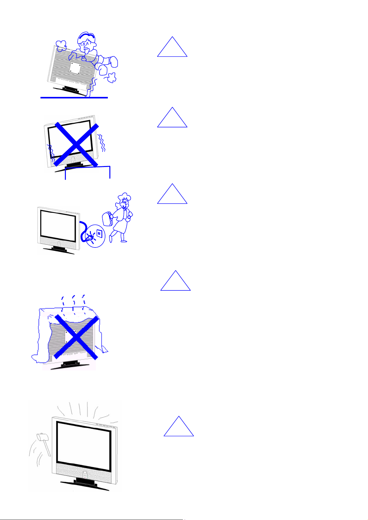
!
Caution
Never stand on, lean on, push suddenly the product or its
stand. You should pay special attention to children to children.
!
Caution
Do not place the main unit on an unstable cart stand, shelf or
table. Serious injury to an individual, and damage to the
television, may result if it should fall.
!
When the product is not used for an extended period of time, it
Caution
is advisable to disconnect the AC power cord from the AC
outlet.
!
Avoid exposing the main unit to direct sunlight and other
source of the heat. Do not stand the television receiver
directly on other produces which give off heat. E. g. video
cassette players,Audio amplifiers. Do not block the
ventilation holes in the back cover. Ventilation is essential to
prevent failure of electrical component. Do not squash power
supply cord under the main unit.
!
Caution
Caution
The LCD panel used in this product is made of glass.
Therefore, it can break when the prod uct is dropped or
applied with impact. Be careful not to be injured by
broken glass pieces in case the LCD panel breaks.
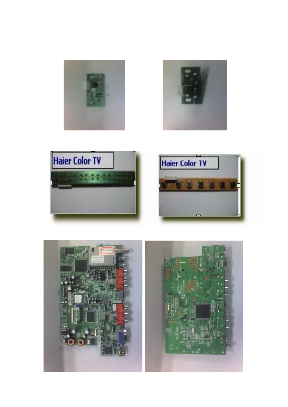
Images of Module and Circuit Boards
1.images of Remote Board Subassembly
2.images of Control Panel Subassembly
3.images of Main Board
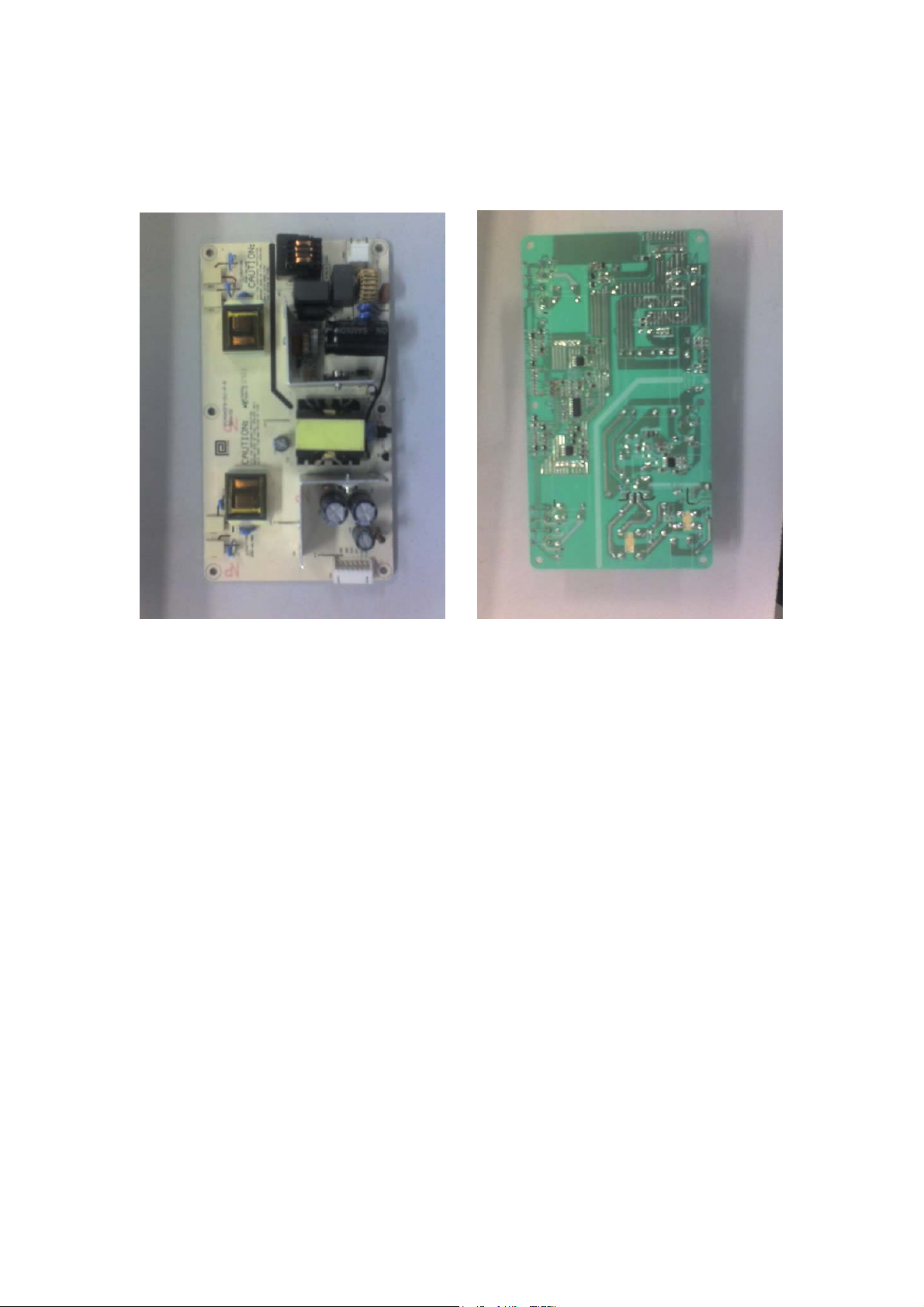
4.images of Power Supply
Key IC Description
1.UOC3
Function:TV signal processor with Teletext and Nicam
PIN SYMBOL DESCRIPTION
1 VSSP2 ground
2 VSSC4 ground
3 VDDC4 Digital supply to SDACs(1.8V)
4 VDDA3(3.3V) Supply(3.3V)
5 VREF_POS_LSL Positive reference voltage SDAC(3.3V)
6 VREF_NEG_LSL+HPL Negative reference voltage SDAC(0V)
7 VREF_POS_LSR+HPR Positive reference voltage SDAC(3.3V)
8 VREF_NEG_HPL+HRP Negative reference voltage SDAC(0V)
9 VREF_POS_HPR Positive reference voltage SDAC(3.3V)
10 XTALIN Crystal oscillator input
11 XTALOUT Crystal oscillator output
12 VSSA1 ground
13 VGUARD/SWIO
14 DECDIG Decoupling digital supply
15 VP1 1st supply voltage TV-processor(+5V)
16 PH2LF Phase-2 filter
17 PH1LF Phase-1 filter
18 GND1 Ground 1 for TV-processor
19 SECPLL SECAM OLL decoupling
20 DECBG Bandgap decoupling
21 EWD/AVL East-West drive output or AVL capacitor
22 VDRB Vertical drive B output
23 VDRA Vertical drive A output
24 VIFIN1 IF input 1
25 VIFIN2 IF input 2
26 VSC Vertical sawtooth capacitor
27 IREF Reference current input
28 GNDIF Ground connection for IF amplifier
29 SIFN1/DVBIN1 SIF input 1/ DVB input 1
30 SIFN2/DVBIN2 SIF input 2/ DVB input2
31 AGCOUT Tuner AGC output
32 EHTO EHT/over voltage protection input
33
AVL/SWO/SSIF/REFO/
REFIN
V-guard input/I/O switch (e.g.4mA current sinking
capability for direct drive of LEDs)
Automatic volume leveling/switch output/sound IF
input sub-carrier reference output/external reference
signal mixer for DVB operation
34 AUDIOIN5L Audio-5 input(left signal)
35 AUDIOIN5R Audio-5 input(right signal)
36 AUDOUTSL Audio output for SCART/CINCH(left signal)
37 ADUOUTSR Audio output for SCART/CINCH(right signal)
38 DECSDEM Decoupling sound demodulator
39
40 GND2 Ground 2 for TV processor
41 PLLIF IF-PLL loop filter
42 SIFAGC/DVBAGC
43 DVBO/IFVO/FMRO
44 DVBO/FMRO Digital Video Broadcast output/IF video output
45 VCC8V 8 Volt supply for audio switches
46 AGC2SIF AGC capacitor second sound IF
47 VP2 2th supply voltage TV processor(+5V)
48 IFVO/SVO/CVBSI IF video output/selected CVBS out/CVBS input
49 AUDIOIN4L Audio-4 input(left signal)
50 AUDIOIN4R Audio-4 input(right signal)
51 CVBS4/Y4 CVBS4/Y4 input
52 C4 Chroma-4 input
53 AUDIOIN2L/SSIF Audio 2 input (left signal)/sound IF input
54 AUDIOIN2R Audio 2 input (right signal)
55 CVBS2/Y2 CVBS2/Y2 input
56 AUDIOIN3L Audio 3 input(left signal)
57 AUDIOIN3R Audio 3 input(right signal)
58 CVBS3/Y3 CVBS 3/Y2 input
59 C2/C3 Chroma-2/3 input
60 AUDOUTLSL Audio output for audio power amplifier (left signal)
61 AUDOUTLSR Audio output for audio power amplifier (right signal)
62 AUDOUTHPL Audio output for headphone channel (left signal)
63 AUDOUTHPR Audio output for headphone channel (right signal)
64 CVBSO/PIP CVBS/PIP output
65 SVM Scan velocity modulation output
66 FBISO/CSY
67 HOUT Horizontal output
68 VSScomb Ground connection for comb filter
69 VDDcomb Supply voltage for comb filter(5V)
70 VIN(R/Prin2/Cx)
71 UIN(B/PBIN2) U-input for YUV interface(2th B input/PB input)
QSS0/AMOUT/AUDEEM QSS inter-carrier output/AM
output/deemphasis(front-end audio out)
AGC sound IF/internal-external AGC for DVB
applications
Digital Video Broadcast output/IF video output/FM
radio output
Flyback input/sandcastle output or composite H/V
timing output
V-input for YUV interface(2th 日 input/Pr input or Cx
input)
72
YIN(G/YIN2/CVBS-Yx) Y-input for YUV interface(2th G input/Y input or
CVBS/Yx input)
73 YSYNC Y-input for sync separator
74 YOUT Y-output (for YUV interface)
75 UOUT(INSSW2)
U-output for YUV interface(2
input)
nd
RGB/YPbPr insertion
76 VOUT(SWO1)
V-output for YUV interface(general purpose switch
output)
77 INSSW3 3rd RGB/YPbPr insertion input
78 R/PRIN3 3rd R input/Pr input
79 G/YIN3 3rd G input/Y input
80 B/PbIN3 3rd B input/P5 input
81 GND3 Ground 3 for TV-processor
82 VP3 3rd supply for TV processor
83 BCLIN Beam current limiter input
84 BLKIN Black current input
85 RO Red output
86 GO Green output
87 BO Blue output
88 VDDA1
Analog supply for TCG u-Controller and digital supply
for TV-processor(+3.3V)
89 VREFAD_NEG Negative reference voltage (0V)
90 VREFAD_POS Positive reference voltage (3.3V)
91 VREFAD Reference voltage for audio ADCs(3.3/2V)
92 GNDA Ground
93 VDDA(1.8V) Analogue supply for audio ADCs(1.8v)
94 VDDA2(3.3V) Supply voltage SDAC(3.3V)
95 VSSadc Ground for video ADC and PLL
96 VDDadc(1.8V) Supply voltage video ADC and PLL
97 INTO/P0.5
External interrupt 0 or port 0.5(4mA current sinking
capability for direct drive of LEDs)
98 P1.0/INT1 Port 1.0 or external interrruput1
99 P1.1/T0 Port 1.1 or Counter/Timer 0 input
100 VDDC2 Digital supply to core(1.8V)
101 VSSC2 ground
102 P0.4/I2SWS Port 0.4 or I2S word select
103 P0.3/I2SCLK Port 0.3 or I2S clock
104 P0.2/I2SDO2 Port 0.2 or I2S digital output 2
105 P0.1/I2SDO1 Port 0.1 or I2S digital output 1
106 P0.0/I2SD1I/O Port 0.0 or I2S digital input 1 or I2S digital output
107 P1.3/T1 Port 1.3 or Counter/Timer 1 input
108 P1.6/SCL Poet 1.6 or I2C-bus clock line
109 P1.7/SDA Port 1.7 or I2C-bus data line

110 VDDP(3.3V)
111 P2.0/TPWM Poet 2.0 or tuning PWM output
112 P2.1/PWM0 Port 2.1 or PWM0 output
113 P2.2/PWM1 Port 2.2 or PWM1 output
114 P2.3/PEM2 Port 2.3 or PWM2 output
115 P3.0/ADC0 Port 3.0 or ADC0 input
116 P3.1/ADC1 Port 3.1 or ADC1 input
117 VDDC1 Digital supply to core(+1.8)
118 DECV1V8 Decoupling 1.8V supply
119 P3.2/ADC2 Port 3.2 or ADC2 input
120 P3.3/ADC3 Port 3.3 or ADC3 input
121 VSSC/P Digital ground for u-Controller core and periphery
122 P2.4/PWM3 Port 2.4 or PWM3 output
123 P2.5/PWM4 Port 2.5 or PWM4 output
124 VDDC3 Digital supply to core(1.8v)
125 VSSC3 ground
126 P1.2/INT2 Port 1.2 or external interrupt 2
127 P1.4/RX Port 1.4 or UART bus
128 P1.5TX Port 1.5 or UART bus
Supply to periphery and on-chip voltage
regulator(3.3V)
2.RTD2023B
PIN SYMBOL DESCRIPTION
1 APLL_GND Ground for multi-phase PLL
2 APLL_VDD Power for multi-phase PLL
3 PLL_TEST1 Test Pin 1 Power-on-latch for MCU crystal location
4 PLL_TEST2 Test Pin 2 Power-on-latch for crystal in frequency
5 TMDS_TST TMDS_TEST Pin Power-on-latch for host interface type
6 REXT Impedance Match Reference.
7 TMDS_VDD TMDS power
8 RX2P Differential Data Input
9 RX2N Differential Data Input
10 TMDS_GND TMDS ground
11 RX1P Differential Data Input
12 RX1N Differential Data Input
13 TMDS_VDD TMDS power
14 RX0P Differential Data Input
15 RX0N Differential Data Input
16 TMDS_GND TMDS ground
17 RXCP Differential Data Input
18 RXCN Differential Data Input
19 AVS0 ADC vertical sync input 5V tolerance Power from PIN

13
20 AHS0 ADC horizontal sync input Adjustable Schmidt trigger
5V tolerance Power from PIN 13
21 ADC_VDD ADC Power
22 ADC_GND ADC Ground
23 B0+ 1st Positive BLUE analog input (Pb+)
24 B0 1st Negative BLUE analog input (Pb-)
25 SOG0 1st Sync on Green
26 G0+ 1st Positive GREEN analog input (Y+)
27 G0 1st Negative GREEN analog input (Y-)
28 R0+ 1st Positive RED analog input (Pr+)
29 R0 1st Negative RED analog input (Pr-)
30 V7 Video8 bit 7
31 V6 Video8 bit 6
32 V5 Video8 bit 5
33 V4 Video8 bit 4
34 V3 Video8 bit 3
35 V2 Video8 bit 2
36 V1 Video8 bit 1
37 ADC_GND ADC Ground
38 ADC_VDD ADC Power
39 V0 Video8 bit 0
40 VCLK Video8 Clock
41 NC -42 NC -43 NC -44 NC -45 NC -46 Digital 1.8V Ground GNDK
47 Digital 1.8V Power VCCK
48 COUT Crystal out
49 PWM2 Pulse width modulation output port2
50 DDCSCL1(ADC) Open drain (Internal 75K pull high)
51 DDCSDA1(ADC) Open drain (Internal 75K pull high)
52 DCLK CLOCK
53 DENA DATA ENABLE
54 BGRN0 Display B-port Green Data 0
55 BGRN1 Display B-port Green Data 1
56 BRED0 Display B-port Red Data 0
57 BRED1 Display B-port Red Data 1
58 BJT_B Embedded regulator P type BJT control pin out
59 Pad 3.3V Power PVCC
60 Pad 3.3V Ground PGND

61 BBLU7 Display B-port Blue Data 7
62 BBLU6 Display B-port Blue Data 6
63 BBLU5 Display B-port Blue Data 5
64 BBLU4 Display B-port Blue Data 4
65 BBLU3 Display B-port Blue Data 3
66 BBLU2 Display B-port Blue Data 2
67 BBLU1 Display B-port Blue Data 1
68 BBLU0 Display B-port Blue Data 0
69 BGRN7 Display B-port Green Data 7
70 BGRN6 Display B-port Green Data 6
71 NC -72 NC -73 BGRN5 Display B-port Green Data 5
74 BGRN4 Display B-port Green Data 4
75 BGRN3 Display B-port Green Data 3
76 BGRN2 Display B-port Green Data 2
77 BRED7 Display B-port Red Data 7
78 BRED6 Display B-port Red Data 6
79 BRED5 Display B-port Red Data 5
80 BRED4 Display B-port Red Data 4
81 BRED3 Display B-port Red Data 3
82 BRED2 Display B-port Red Data 2
83 Pad 3.3V Power PVCC
84 Pad 3.3V Ground PGND
85 ABLU7 Display A-port Blue Data 7
86 ABLU6 Display A-port Blue Data 6
87 ABLU5 Display A-port Blue Data 5
88 ABLU4 Display A-port Blue Data 4
89 ABLU3 Display A-port Blue Data 3
90 ABLU2 Display A-port Blue Data 2
91 ABLU1 Display A-port Blue Data 1
92 ABLU0 Display A-port Blue Data 0
93 AGRN7 Display A-port Green Data 7
94 AGRN6 Display A-port Green Data 6
95 NC -96 NC -97 AGRN5 Display A-port Green Data 5
98 AGRN4 Display A-port Green Data 4
99 AGRN3 Display A-port Green Data 3
100 AGRN2 Display A-port Green Data 2
101 ARED7 Display A-port Red Data 7
102 ARED6 Display A-port Red Data 6
103 ARED5 Display A-port Red Data 5
 Loading...