


DX-LTDVD19-09
@ (2008)(Haier Electronic Company Limited)
All rights reserved. Unauthorized copying and distribution is a
violation of law.
1

WARNING
This service information is designed for experienced repair technicians only and is not designed for use
by the general public. It does not contain warnings or cautions to advise non-technical individuals of
potential dangers in attempting to service a product. Products powered b electricity should be serviced
or repaired only by experienced professional technicians. Any attempt to service or repair the product
deal with in this service information by anyone else could result in serious injury or death
.
CONTENT
1. SPECIFICATIONS…………………………………………………………………… ……………….. ..3
2. WAINING……………………………………………………………………………………… ………… 4
3. LOCATION OF CONTROLS AND COMPONENTS……………………………………… ……..….. 6
3.1. Board Location……………………………….. ……………… ……………………… …….……..6
3.2 Main Board & AV Board……………………………….. …………………………………… …….7
3.3 Power Board……………………………….. ………………………………………………… ……9
3.4 LCD Panel…………………..……………………………….. ……………………………… ...….10
4.
External Equipment Connections…………………………………………………………………..….11
5. OPERATION INSTRUCTIONS………………………………………………………………………….15
5.1 Front Panel Controls……………………………….. ……………………………………….15
5.2 Back Panel Controls……………………………….. ………….………..……. …………….16
5.3 Universal Remote Controller……………………………….. …..………………………….17
6. DISASSEMBLY INSTRUCTIONS……………………………………..…………….……………….18
6.1 Whole Machine………………………………………………...…………………….……….18
6.2 Support Stand Assembly……………………………………………..……... ……....……..19
6.3 Back Cabinet Assembly……………………………………..……….………………..…….20
6.4 Front Cabinet Assembly……………………………..………………………………..……..21
6.5 Miscellaneous Material Assembly………………………………….………………...…....… 21
7. MEASUREMENTS AND ADJUSTMENTS……………………………………………………….…25
8. WIRING CONNECTION DIAGRAM……………………………………………….. ………………32
9. TROUBLESHOOTING GUIDE…………………………………………………..…………....…...33
9.1. Simple check…………………………………………………………..……………….……...33
9.2. Power Supply Board failure check………………………………..……………………….……34
9.3. Main board failure check…………………………………………………………………….…. .35
9.4. Pannel failure ……………..………………………………………………………………...……37
10. MAINTENANCE……………………………………………………………………………...……39
11. CIRCUIT DIAGRAM…………………………………….….……… ……………………… …………. 40
2
1. Specification
Model DX-LTDVD19-09
Screen size 19inch
Aspect ratio 16:10
Resolution 1440*900
Response Time(ms)
Angel of view H:160/V:160
Color display 16,777,216
NO.of preset channels 181
OSD language English/Spanish/French
Color system note 1
Audio system note 2
Audio output
power(Built-in)(W)
Audio output
power(outer)(W)
Total power input(W) <=80W
Voltage range(V)
Power frequency(Hz)
Time of sleep
timer(MINS)
5/10/15/30/60/90/120/180/240
5
2×3W
No
AC120V
60Hz
Net weight(KG) 5
Gross weight(KG) 6.35
Net dimension(MM) 462*179.5*388.5
Packaged
dimension(MM)
Notes:
1.NTSC:
2. M standard: each channel bandwidth is 6 MHz and the frequency of audio is 4.5 MHz higher than the
frequency of video.
Standards Developed by National TV Standards Committee
522*203*438
3
2. Warning
WARNING
RISKELECTRIC SHOCK
DONOT OPEN
WARNING: To reduce the risk of electric shock don’t remove cover or back.
No user-serviceable parts inside refer service to qualified service personnel.
Safety of operators has been taken into consideration at the design and manufacture phase, but
inappropriate operation may cause electric shock or fire. To prevent the product from being damaged,
the following rules should be observed for the installation, use and maintenance of the product. Read
the following safety instruction before starting the operation.
The User Manual uses the following symbols to ensure a safe operation and preventany damage to
operators or properties:
THIS SYMBOL INDICATES THAT HIGH VOLTAGE IS PRESENT INSIDE. IT IS
DANGEROUS TO MAKE ANY KING OF CONTACT WITH ANY INSIDE PART OF THIS
PRODUCT.
THIS SYMBOL INDICATES THAT THERE ARE IMPORTANT OPERATING AND
MAINTENANCE INSTRUCTIONS IN THE LITERATURE ACCOMPANYING THE
APPLIANCE.
FC C STATEMENT
This equipment has been tested and found to comply with the limits for a Class B digital device,
pursuant to Part 15 of the FCC Rule. These limits are designed to provide reasonable protection
against harmful interference in a residential installation. This equipment generates, use and can radiate
radio frequency energy and, if not installed and used in accordance with the instructions, may cause
harmful interference to radio communications. However, there is no guarantee that interference with
not occur in a particular installation. If this equipment does cause harmful interference to radio or
television reception, which can be determined by turning the equipment off and on, the user is
encourage to try to correct the interference by one or more of the following measures:
*Reorient or relocate the receiving antenna.
*Increase the separation between the equipment and receiver.
*Connect the equipment into an outlet on a circuit different from that to which the receivers
connected.
*Consult the dealer or an experienced radio/TV technician for help.
This device compiles with Part 15 of the FCC Rules. Operation is subject to the following two
conditions: (1) This device may be not cause harmful interference, and (2) this device must accept any
interference received, including interference that may cause undesired operation.
FCC CAUTION:
To assure continued compliance and possible undesirable interference, the provided ferrite cores must
be used when connecting this plasma display to video equipment; and maintain at least 40cm spacing
to other peripheral device.
CANADIAN NOTICE:
This Class B digital apparatus compiles with Canadian ICES-003.
4

IMPORTANT SAFETY INSTRUCTIONS
Read all of the instructions before using this appliance. When using this appliance, always
exercise basic safety precautions, including the following:
1) Save these Instructions ---the safety and operating instructions should be retained for future
reference.
2) All warning on the appliance and in the operating instructions should be followed.
3) Cleaning --- Unplug from the wall outlet before cleaning. Do not use liquid cleaners or aerosol
cleaners. Use only dry cloth for cleaning.
4) Attachments ---do not use attachments not recommended by the manufacturer as they may cause
hazards.
5)Water and moisture -- do not place this product near water, for example, near a bathtub, wash bowl,
kitchen sink, laundry tub, in a wet basement, or near a swimming pool.
6) Accessories ---do not place this unit on an unstable cart, stand, tripod, bracket, or table. Use only
with a cart, stand, tripod, bracket, or table recommend by the manufacture, or sold with the unit.
7) Ventilation ---Slots and openings in the cabinets and the back or bottom are provided for ventilation.
These openings must not be blocked. In a built in installation such a bookcase or rack do not install
product unless proper ventilation is provided.
8) Power Source ---this TV should be operated only from the type of power source indicated on the
rating label. If you are not sure of the type of power supply to your home, consult your appliance dealer
or local power company.
9) Do not defeat the safety purpose of the polarized or grounding-type plug. A polarized plug has two
blades with one wider than the other. A grounding type plug has two blades and a third grounding prong.
The wide blade or the third prong are provided for your safety. If the provided plug does not fit into your
outlet, consult an electrician for replacement of the obsolete outlet. To prevent electric shock, ensure
the grounding pin on the AC cord power plug is securely connected.
10) Power cord protection ---Power supply cords should be routed so that they are not likely to be
walked on or pinched by items placed upon or against them. Pay particular attention to cords or plugs,
convenience receptacle, and the point where they exit from the appliance.
11) Lighting precaution ---for added protection for this product during a lighting storm or when it is left
unattended for long period of time, unplug it from the wall outlet and disconnect the antenna or cable
system. This will prevent damage to the product due to lighting and power line surges.
12) Never push objects of any kind into this product through openings as they may touch dangerous
voltage point or short out parts that could result in a fire or electric shock. Avoid spilling liquid of any kind
on the product.
13)Servicing ---do not attempt to service the product by yourself, as opening or removing covers may
expose you to dangerous voltage or other hazards. Refer all servicing to authorized service personnel.
14) Unplug this unit from the wall outlet and refer servicing to qualified service personnel under the
following conditions:
5
a. When the power supply cord or plug is damaged or frayed.
b. If liquid has been spilled, or objects have been fallen into the unit.
c. If the unit has been exposed to rain or water.
d. If the unit does not operate normally by following the operating instructions. Adjust only those
controls that are covered by the operating instructions, as improper adjustment of other controls
may result in damage and will often require extensive work by a qualified technician to restore
the unit to its normal operation.
e. If the unit has been dropped or damaged in any way.
f. When the unit exhibits a distinct change in performance; this indicates a need for service.
15) Heat --- The product should be situated away heat source such as radiators, heat registers,
stoves, or other products (Including amplifiers) that product heat.
16) Overloading ---Do not overload wall outlets and extension cord as this can result in a risk of fire
or electric shock.
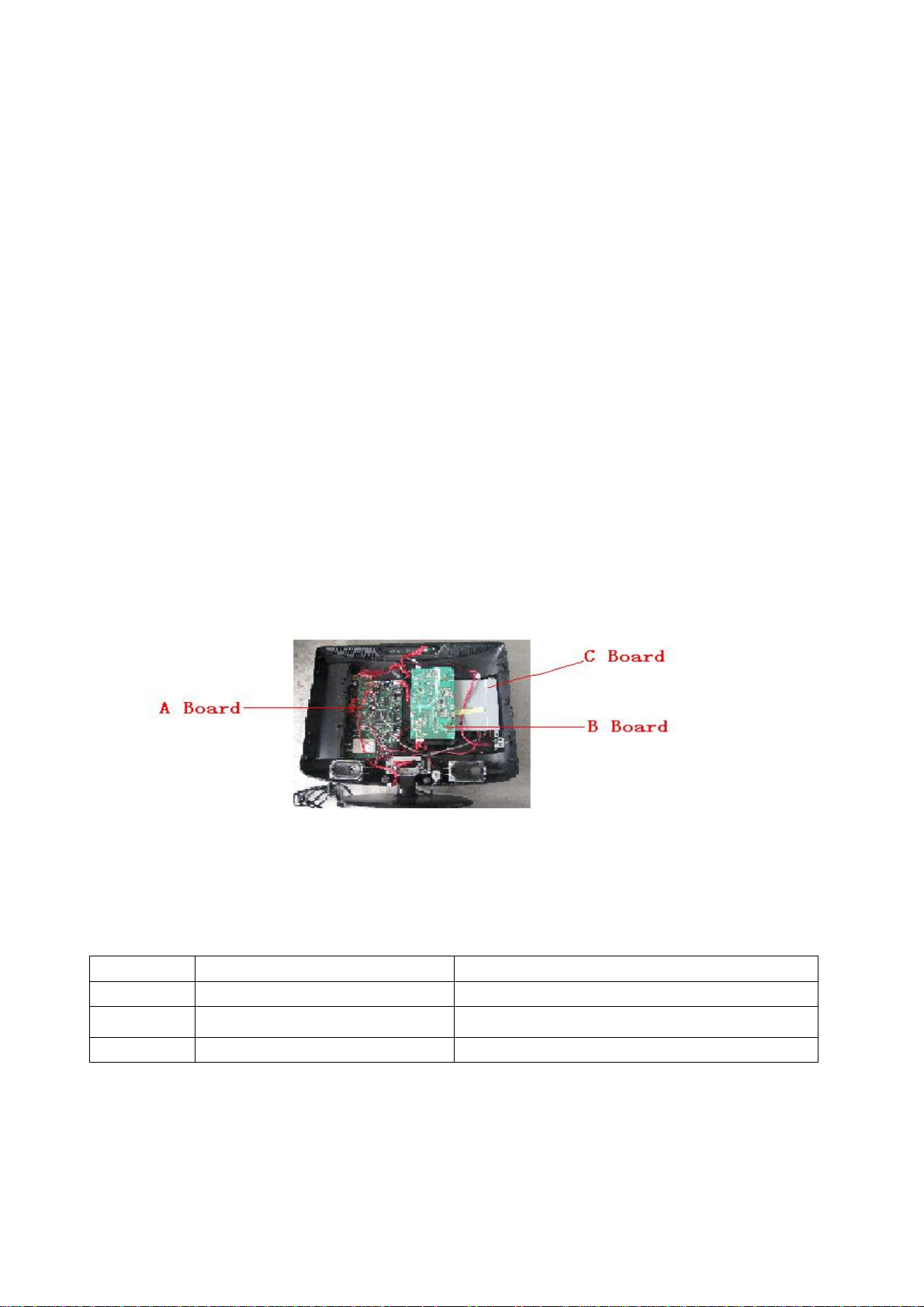
3. LOCATION OF CONTROLS AND COMPONENTS
3.1. Board Location
No. Parts number Description
A Board
B Board Power Board
C Board
6
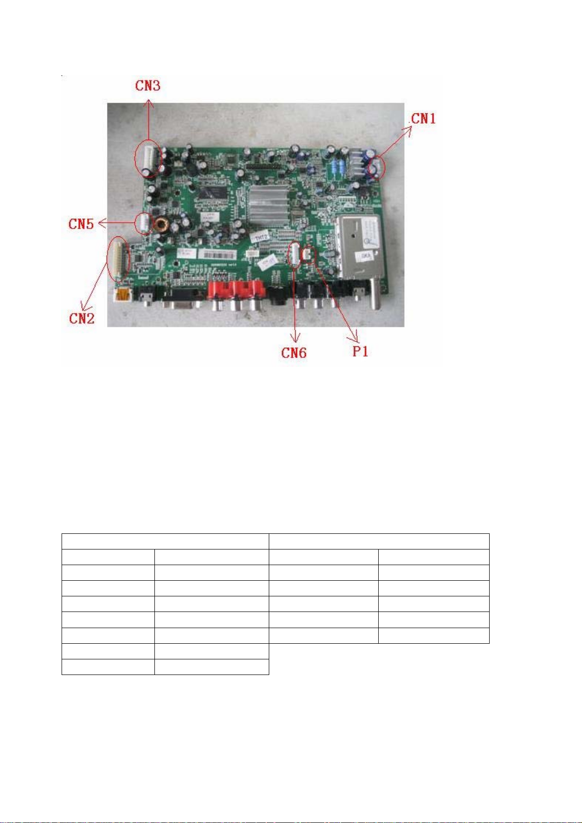
3.2. Main Board & AV Board
3.2.1 Function Description:
Main Board:
Process signal which incept from exterior equipment,then translate into signal that panel can display.
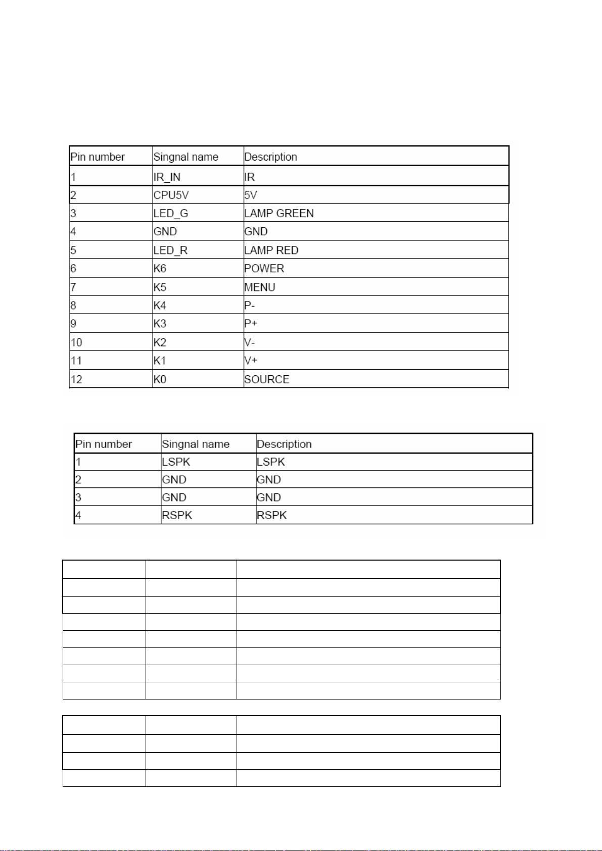
3.2.2 Connector definition
Main board connector
Power connectors (CN3, CN5)
Pin number Signal name Pin number Signal name
1 +12V 1 +12V
2 +12V 2 GND
3 BL 3 GND
4 DIM 4 +5V
5 GND 5 STB
6 GND
7 SW
CN3 CN5
Notes:
CN3-Pin 3: Backlight on/off:
The system can turn on or turn off the backlight of TFT LCD Panel through the power supply unit path.
7
CN3-Pin 7: System power on / standby
System board will use this pin to control system power.
CN3-Pin 4: Control the luminance of backlight
The system can generate the PWN signal to control the strength of TFT LCD Panel’s backlight through
this connector.
Keypad and remote connector (CN2)
Speaker connector (CN1)
DVD VIDEO Connector: CN6
Pin number Signal name Description
1 GPIO GPIO
2 PB_IN PB1 IN
3 Y_IN Y1_IN
4 GND GND
5 PR_IN PR1 IN
6 GND GND
7 IR DVD IR
DVD AUDIO Connector: P1
Pin number Signal name Description
1 LI YPBPR1L_IN
2 RI YPBPR1R_IN
3 GND GND
8
Other connectors:
1, CN19 to Upgrade the program of MTK5380C (U13) AND FLASH (U17)
J3
+3V3SB
U0RX
U0TX
1
2
3
4
4x1 W/HOUSING
DIP4/W/H/P2.0
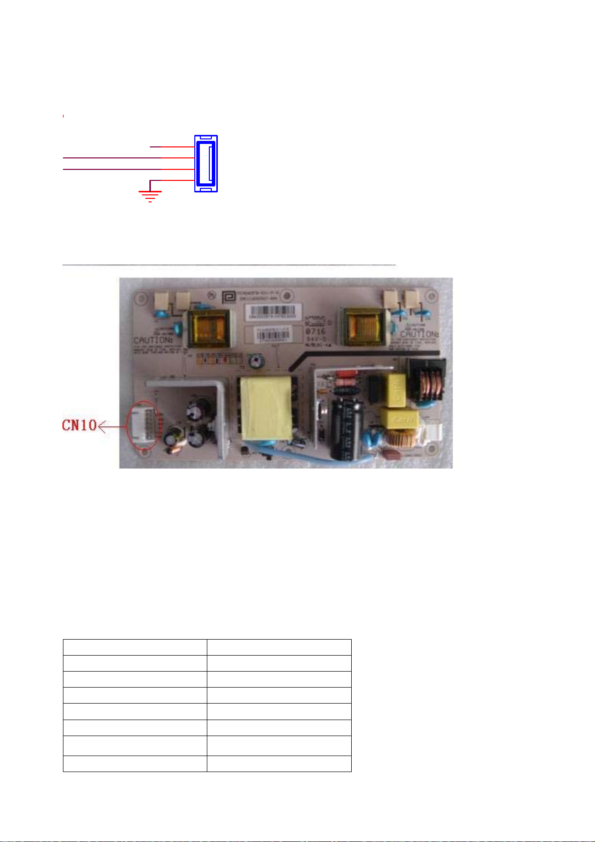
3.3. Power Board
3.3.1 Function Description:
Supply power for Main board, Panel.
3.3.2Connectordefinition
INPUT CONNECTOR (CN6)
CN10 Signal name
1 N
2 GND
3 GND
4 DIM
5 EN
6 +12V
7 +12V
9
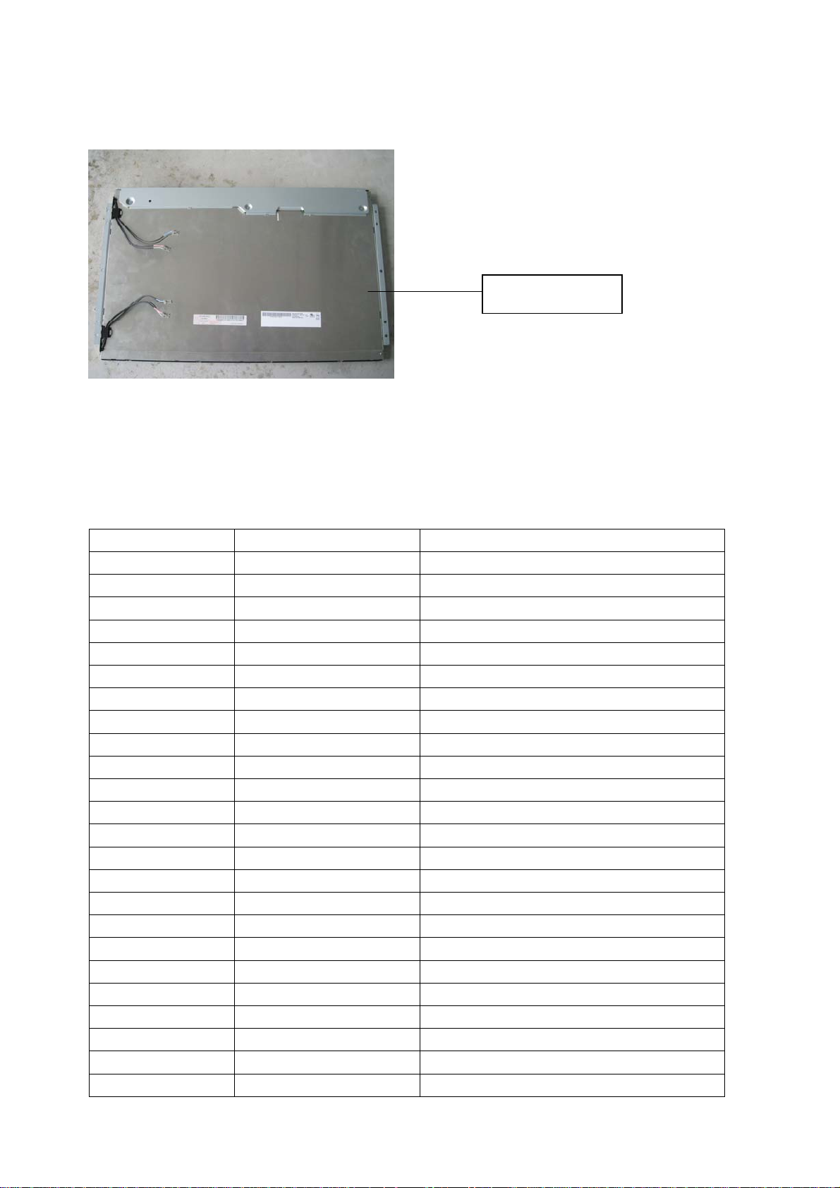
3.4. LCD PANNEL.
AU(T190PW01)
3.4.1 Function Description:
Display the signal.
3.4.2 Connector definition
Pin number Signal name Description
1-3 LVDSVDD Power for panel
4-6 GND Ground
7 A0N LVDS EVEN 0 - Signal
8 A0P LVDS EVEN 0 + Signal
9 A1N LVDS EVEN 1 - Signal
10 A1P LVDS EVEN 1 + Signal
11 A2N LVDS EVEN 2 - Signal
12 A2P LVDS EVEN 2 + Signal
13,14 GND Ground
15 CK1N LVDS EVEN Clock - Signal
16 CK1P LVDS EVEN Clock + Signal
17 A3N LVDS EVEN 3 - Signal
18 A3P LVDS EVEN 3 + Signal
19 A4N LVDS ODD 0 - Signal
20 A4P LVDS ODD 0 + Signal
21 A5N LVDS ODD 1 - Signal
22 A5P LVDS ODD 1 + Signal
23 A6N LVDS ODD 2 - Signal
24 A6P LVDS ODD 2 + Signal
25,26 GND Ground
27 CK2N LVDS ODD Clock - Signal
28 CK2P LVDS ODD Clock + Signal
29 A7N LVDS ODD 3 - Signal
30 A7P LVDS ODD 3+ Signal
10
CN1 (Header):S14B-PH-SM4-TB (D)(LF)(JST) or equivalent.
Pin No. Symnbol Description
1
2
3
4
5
6
13
14
25
26
7-12
15
16
17
18
VBL
GND
LVDS
EVEN
+5.0V Power input
Ground
LVDS EVEN Signal
19-24
27
28
29
30
LVDS
ODD
LVDS ODD Signal
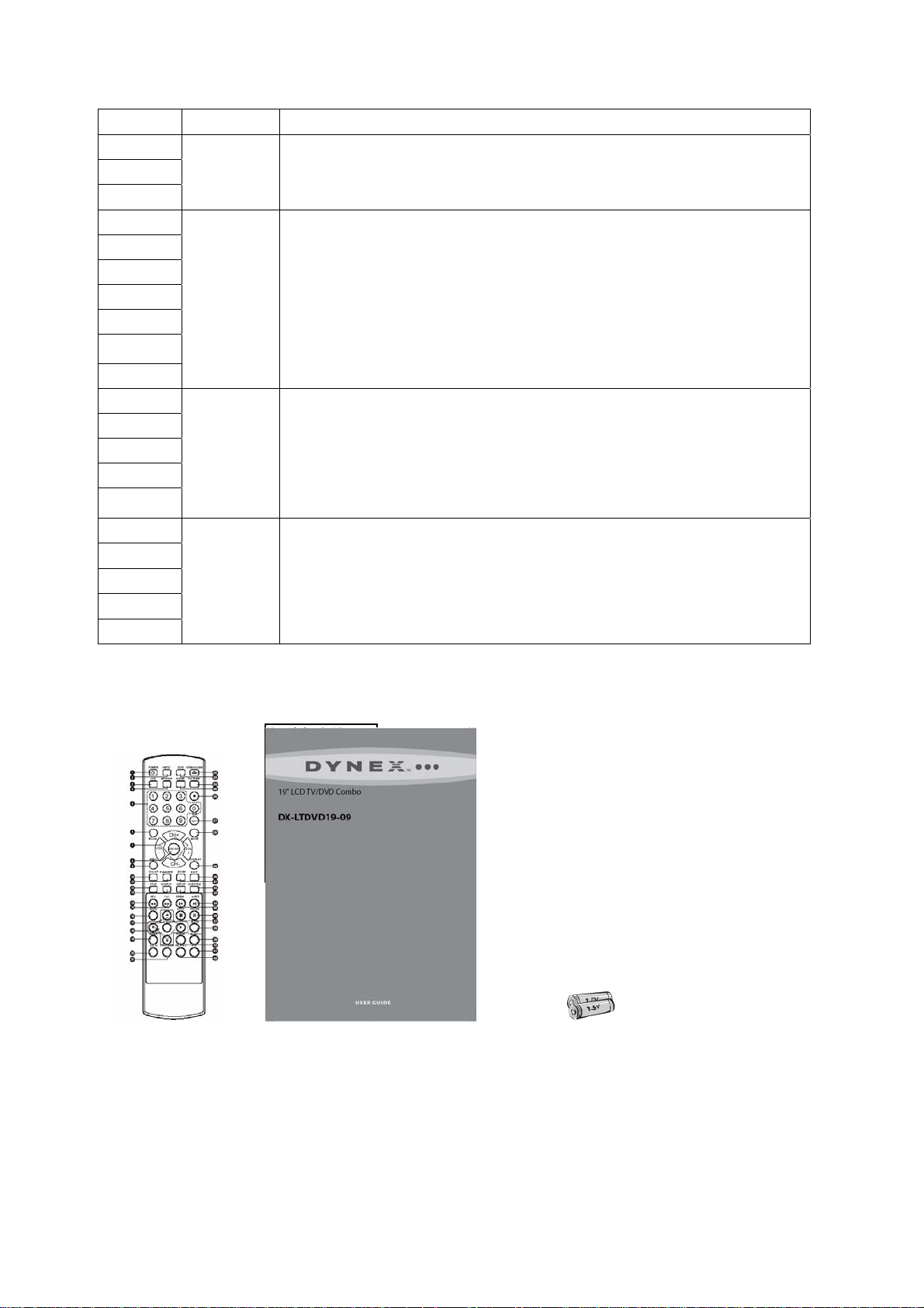
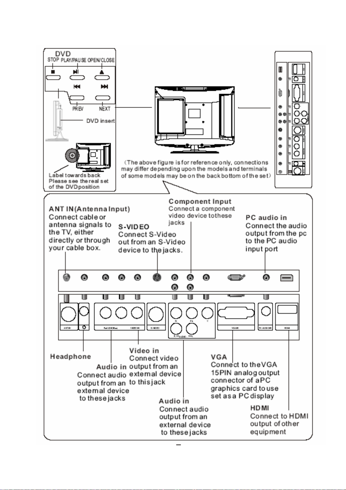
4. External Equipment Connections
Accessories
Remote Control User GUIDE Battery
Antenna Connection
1、 Connect one end of a coaxial cable (not included) to the ANT IN jack on the back of your TV/DVD
combo, then connect the other end of the cable into the antenna or cable TV wall outlet.
11
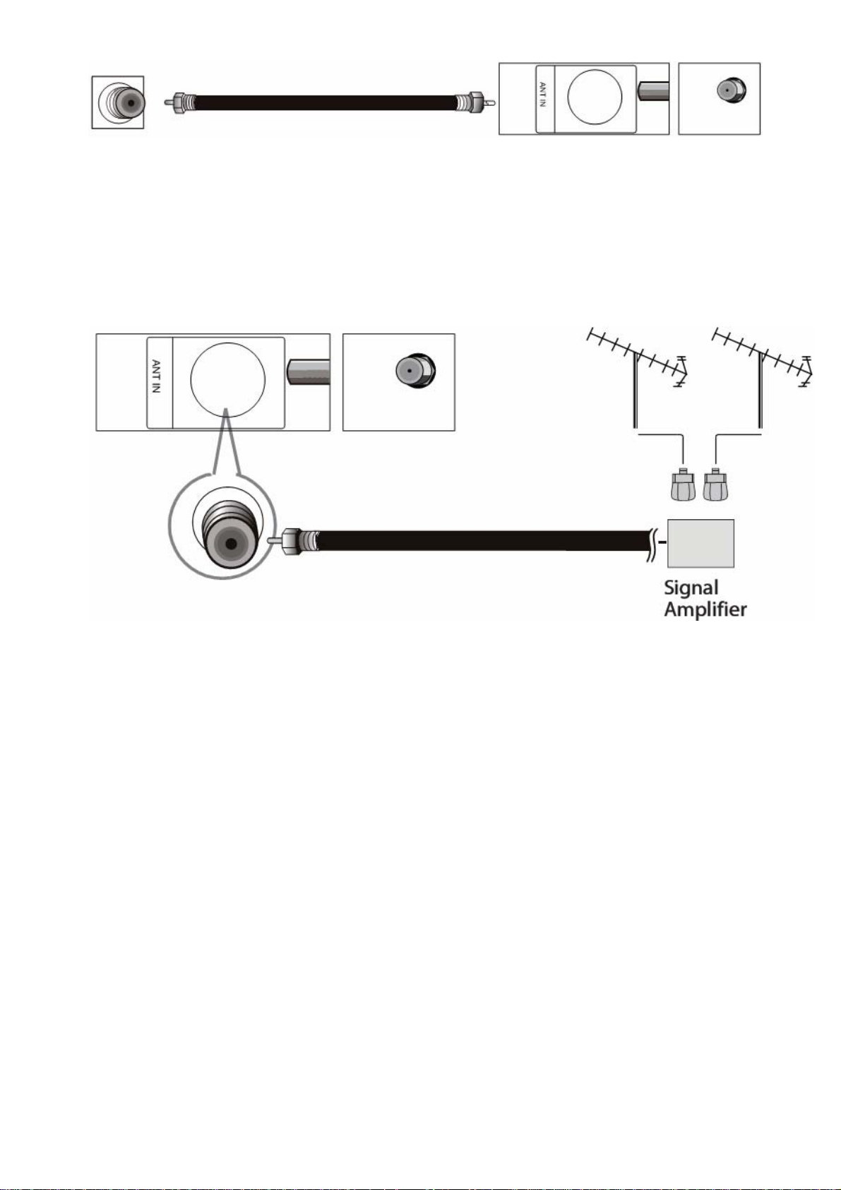
2 、To improve picture quality from an antenna in a poor signal area,
install a signal amplifier.
3、 If you need to split the antenna signal to connect two TVs, install
a two-way splitter.
Choose Your Connection
There are several ways to connect your television, depending on the components you want to connect
and the quality of the signal you want to achieve. The following are examples of some different ways
to connect your TV with different input sources. Choose the connection which is best for you.
12
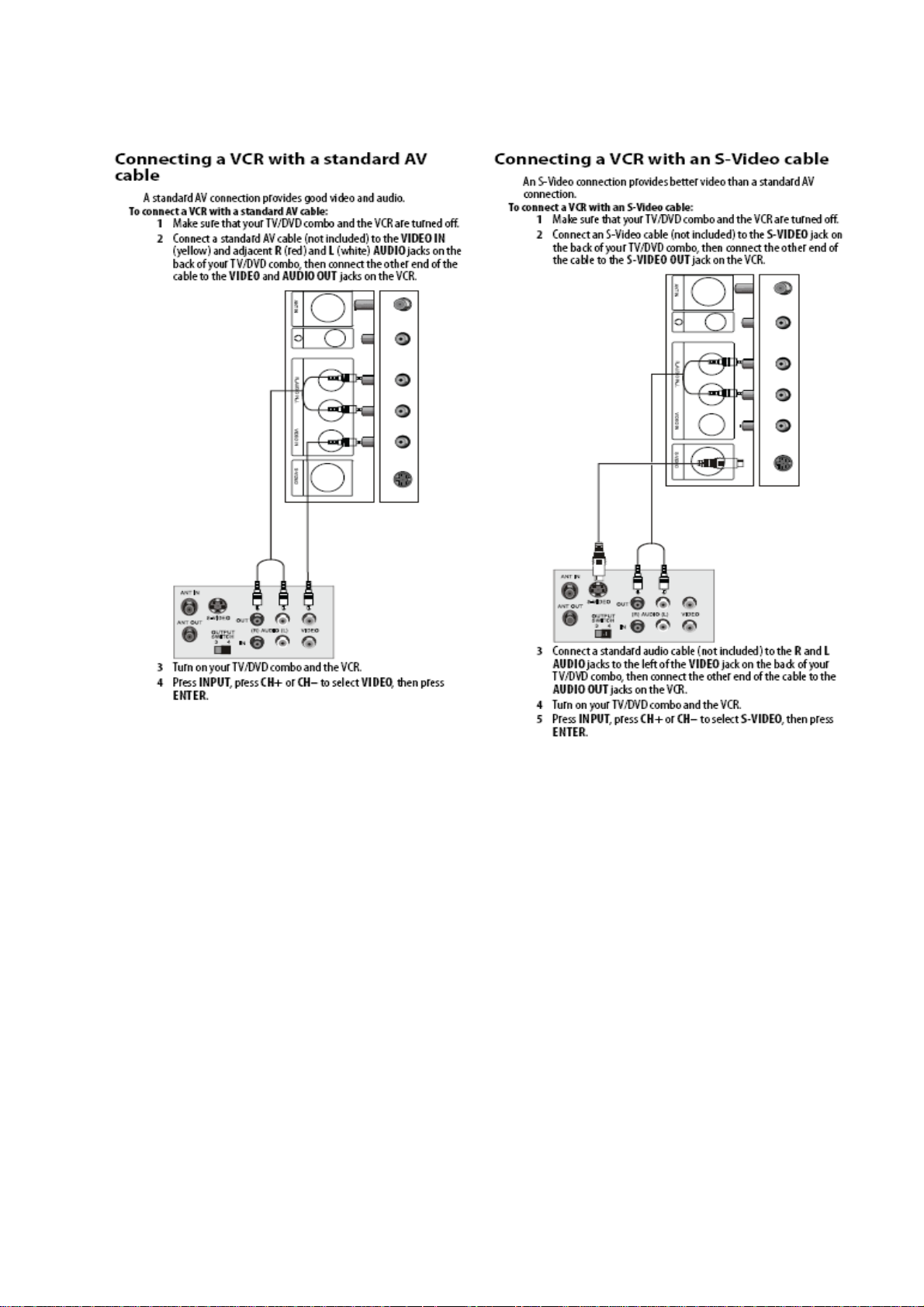
VCR connection
13
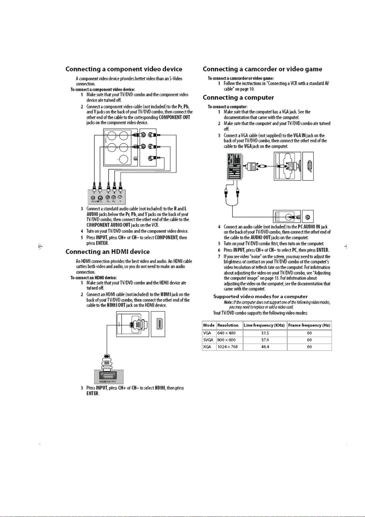
External Equipment Connections
14
5. OPERATION INSTRUCTIONS
Basal information
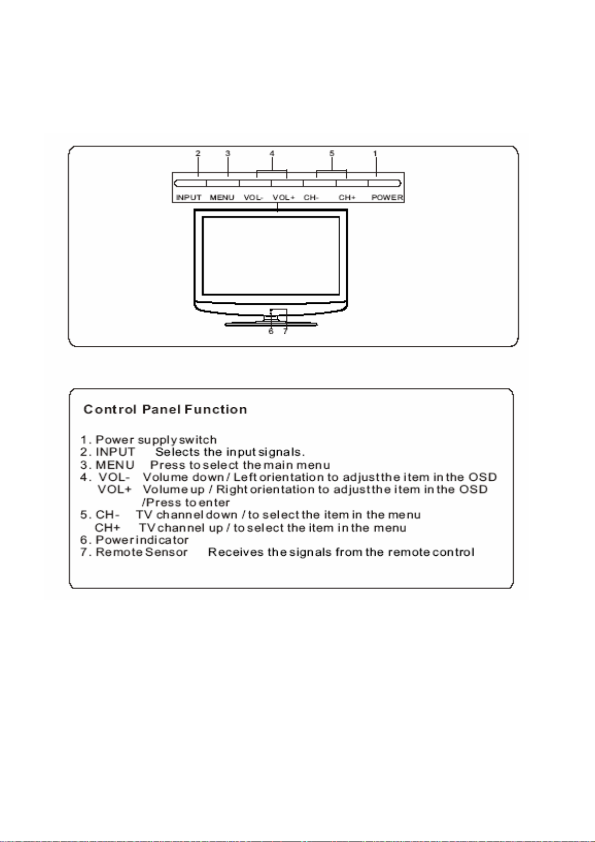
5.1 Front panel controls
15
5.2 Back panel controls
16
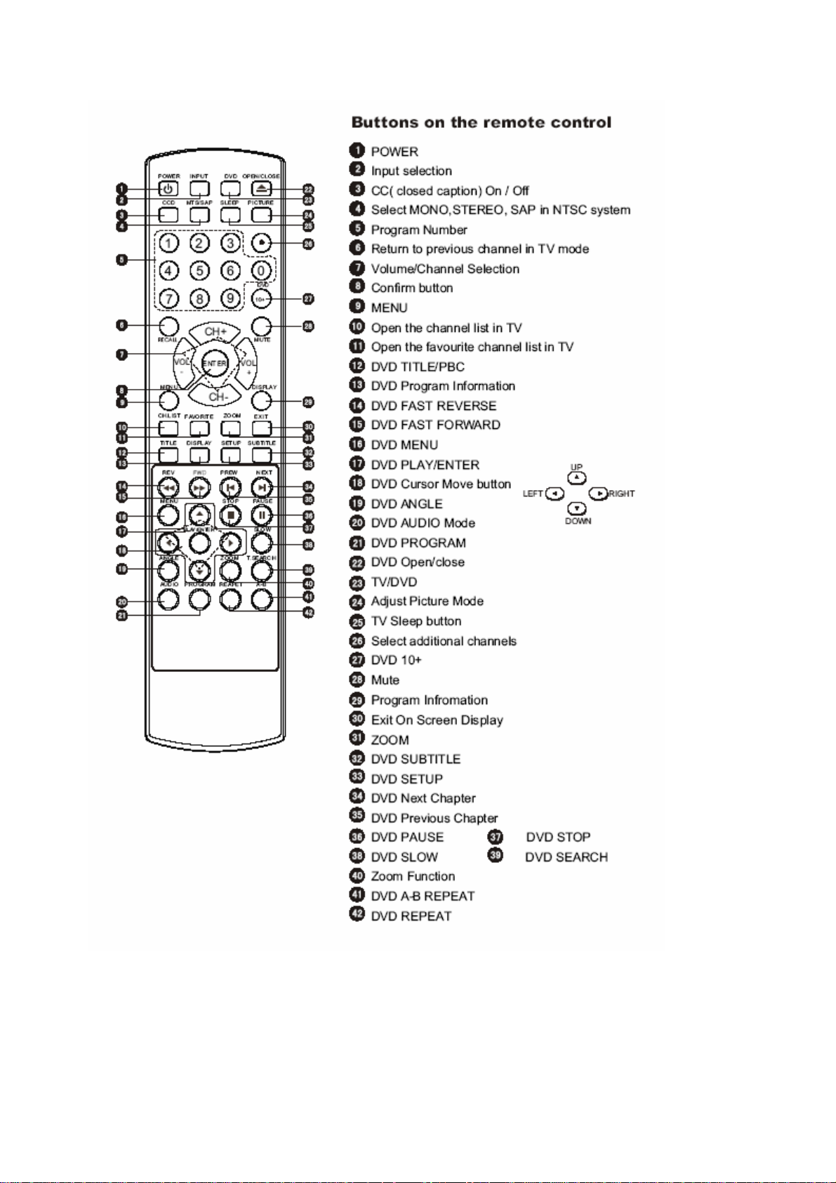
5.3 Universal Remote Controller
17

6. DISASSEMBLY INSTRUCTIONS
6.1.Whole machine
The whole machine includes Packaging Assembly、Front Cabinet Assembly、Back Cabinet Assembly、
Base Assembly、Main board Assembly、Remote Control Board Assembly、Control Board Assembly、
Assembly Material Subassembly、Romote Contral Per-setting Assembly.
1 2 3.1
3.2 3.3 3.4
3.5 3.6 3.7
Components List
NO Name Description Parts number
1 DX-LTDVD19-09
2 Packaging
/
3 TV Set
3.1 Base Borad
3.2 Back Cabinet
3.3
Control PCB
/
18

3.4 Plastic Front Cabinet 0090202142.1
3.5 Remote Control PCB 0091801240
3.6
3.7 DVD DC11Z0E0100D
Main board Assembly
DC11Z0E0100M
6.2. Support Stand Assembly
Assembly
Support Stand
Assembly
Spare parts
number
Support Stand Subassembly 1
=
Locatio
n No.
Spare Parts Name in
English
Support Stand Assembly
Base Board
Rotational Axis 1
Rubber 5
Bolt
Bolt
19
Specificatio
n
1
Support Stand
Assembly 4
GB818-85
M4X16 4
Qty
1

6.3. Back Cabinet Assembly
Components List
Assembly
Spare parts
number
Location
No.
Spare Parts Name in
English
Back Cabinet Assembly
Specification Qty
1
Back Cabinet
Assembly
Back
Back
Button Bracket 1
DVD Control Board bracket 1
Power Board bracket 2
Terminal Board 1
LCD panel bracket 2
Small cover board 1
Bolster 1
DVD shield metal 1
DVD Button Label
Sponge Strip 0.17
Bolt 2
Bolt GB818-85 M3*4 4
Bolt SJ2824-87 ST4X12F 6
Bolt
Bolt
Terminal Lable(black)
Bolt SJ2824-87 ST3*8F
Bolt SJ2824-87 ST3*8F
Bolt SJ2824-87 ST3*8F
Bolt SJ2824-87 ST3X10F
Cabinet Subassembly 1
Cabinet
Screw
Speaker Y47-418-5W/4Ω 2
SJ2824-87 ST4×16F 1
SJ2824-87 ST3X8F 8
1
20
1
2
8
8
3
6

6.4 Front Cabinet Assembly
Assembly
Front Cabinet
Assembly
Spare parts
number
Front Cabinet Assembly 1
Front Cabinet Subassembly 1
Plastic Front Cabinet 1
Transparent Window
Plastic
Bolt SJ2824-87 ST3X10F 2
LCD Pannel T190PW01 1
LOGO
Bolt SJ2824-87 ST3*10F 2
Location
No.
Spare Parts Name in English Specification Qty
board
6.5. Miscellaneous Material Assembly
6.5.1. Location Photo
silk-screen:DYNEX
1
1
21

6.5.2 Components List
Spare parts
number
Miscellaneous
Material
Assembly
Location
No.
Spare Parts
Name in
English
Miscellaneous Material
Assembly 1
LVDS Connection Wire 1
Speaker Connection Wire 1
Connection Wire 1
Power Cord 1
Power Mainboard Inverter
Power Supply Board 1
Left Gasket 1
Right Gasket 1
Magnetic Loop 2
Magnetic Loop 2
ROHS-DVD 1
ROHS-DVD Signal Wire 1
ROHS-DVD Power wire 1
Metal clip 3
Screw 3
Damper Foam
Connective Wire 1
Specification Qty
3
22


7. MEASUREMENTS AND ADJUSTMENTS
The way to the factory mode menu:
1st, press nemu,
2sec, input 8893,
Finished these operations ,system will be into the factory mode menu.
IF want to exit this factory menu,please press the botton”Exit” in the remoter.
7.1 Version ,S/N, Panel Resoution
Version:The first line is the model Name and the second line is current software version.
23

7.2 Video
7.2.1,Auto Color
The option could only be used in the VGA and Component model. When we found the color in the two
models was abnormal. Then we can use the function to adjust it automatically.
7.2.2,Color Temperature
The function could adjust the Color Temperature., used when debugging.
7.3 Audio
24

Dolby Banner: When turn it “ON”, the model will be in Dolby authentication state.
Compression: Compression style. RF: atv line:AV/S-Video/YPbPr/VGA
Compression Factor: Compression state.
Downmix: output model. MTS System: used when debugging. The parameters only used when
debugging, no need to be modified.
7.4 Channel
Range Scan: The function could make it to search the channels by differentiation the analog and
digital channels.
25

Single RF Scan: Search channels in the frequency scope set in advance.
Factory Scan: According to ANTENNA-ANALOG---〉ANTENNA-DIGITAL---〉CABLE- ANALOG---〉
CABLE- DIGITAL to search channels, used only in project debugging.
26

Tuner Diagnostic: Project debugging setting, used to inspect the audio function.
7.5Gamma
Gamma:
Bright:GAMMA0.8 Middle:default settings in the program Dark:GAMMA1.2
27

7.6 Backlight
Backlight: adjust the backlight.
7.7 Function
Burning Mode:
Turn it “ON” to enter the aging model, This is for factory run-in testing. The screen would display red,
green, blue and black screen repeatedly. Each color screen could be exam at that time.
28

Clean Storage:The function could make the model turn back to the factory default setting.
Remark:
The date of the chart only is a example, please don’t adjust the factory mode base on it.
29

8. WIRING CONNECTION DIAGRAM
30

9. TROUBLE SHOOTING GUIDE
9.1. Simple check
No Picture,no sound
Blank screen
No sound
Poor sound
No picture in some channel
No color for some channel
program(black and white)
Verify if the television is properly plugged
Verify if the television is properly supplied power
Verify if electricity is available
Verify if correct signals are input
Press INPUT button to change signal input to TV input
Restart the television of power supply is interrupted
Press Mute button and verify if Mute mode is set.
Switch to otger channel and verify if the same problem happens.
Press VOL+ button to see of he problem can be solved.
Verufy if sound system is correct .Refer to some chapter for
adjust.
Verify if correct channel is selected.
Adjust the antenna.
Make adjustments by Fine Tune and MANUAL Scan.
Verify if the same problem exists in other channels.
check out of picture and sound system.
Refer to relative instructions in the Manual for color adjust.
Spots with some or all pictures
Horiaontal/vertical bars or picture
shaking
Television out of control
Verify if the antennal is correctly connected.
Verify if the antennal is in good condition.
Make fine adjustment of channel.
Check for local interference such as an electrical appliance or
power tool.
Disconnect the television from power supply and 10 seconds
later, connect the television to the power supply. If the problem
still exists, contact authorized after-sales service for technical
assistance.
31

9.2 Power Supply Board failure check
State: No power
First, check cables which connect with PSU, then check as follows
1) Check PSB input voltage(AC input)
voltage : ~120V
connector : CN7
2)Check PSB output voltage orderly:
voltage : +12V ,+12V
connector:CN3(P6,P7)
32

9.3 Main board failure check
State: No picture
Pass
Pass
Pass
Pass
Pass
No Sound
(All Mode)
Check the input
Source
Check the input/output
Of IC U13 of Main B/D
Check the input/output
Of IC U55 of Main B/D
Check the input/output
Of IC U2 of Main B/D
Check the Speaker
Check the Sperker
wire
Fail
Fail
Fail
Fail
Fail
Change Source input
Re-soldering or change
IC U13
Re-soldering or change
IC U55
Re-soldering or change
IC U2
Change the Speaker
33

State:No picture
No Raster
on Panel
Check the backlight
B/D
Pass
Check the input/output of
jack CN3 of Main B/D
Pass
Check the input/output of
Jack CN4 of Main B/D
Pass
Check the Panel
wire
Pass
Change the panel
Fail
Fail
Fail
Fail
Change the backlight B/D
Re-soldering or change
IC UA1 and RNA1-17
Re-soldering or change
IC U13
Change the Panel wire
34

9.4 Panel failure
Failure Mode
Part Name Description Phenomena Failure cause
Block Defect :TCP cracking or cracking
Dim or L/D :TCP Sunken
:TCP lead cracking
:ACF bonding short
:Awful environment and something electric enter into
LCD
:Mis-align between TCP and Panel
:Panel failure
:TCP failure
TCP
V B/D Vertical bar
V Dim
V L/D
H B/D
H Dim
Vertal gray
line
Vertical color
line(light or
dark forever)
Horizontal
bar
Horizontal
gary line
Horizontal
H L/D
line(light or
dark forever)
Failure Mode
Part Name Description Phenomena Failure cause
Bright dot dark
dot in pannel
Bladder in
Polarizer
Polarizer Scratch
Incoming Inspection Standard
Bladder between Polarizer and top glass
Tine or rigidity arose
Panel or
Polarlzer
Dot Defect
Polarizer
Bubble
Polarizer
Scratch
F/M inside
Polarizer
Eyewinker inside
Polarizer
Eyewinker inside Polarizer
35

Circuit
Abnormal
Display
Flashing
Abnormal Display
Bright and dark
display alternately
1. Chip lose action
2. IC ahort or jointiog bad
3. Pannel and vsc connect bad
White
Screen
B/L normal, only
white screen
display
Failure Mode
Part Name Description Phenomena Failure cause
Maybe caused by surge current and EDS
Black
Screen
B/L normal, only
Black screen
display
Circuit
FIIcker Crosstalk
LCD Vcom imbalance
Abnormal
Color
Only color
abormal
Capacitance improper bring crosstalk inside LCD
pannel
Abnormal
Color
Only color
abnormal
1. Chip lose action
2. IC short or jointion bad
3. Pannel and vsc connect bad
Failure Mode
Part Name Description Phenomena Failure cause
Mechanlcal
Nolse
Ripple Connectric circle
B/L off B/L lose action
B/L dark B/L brightness
When turn
panel,appear
cacophony
darker than normal
Caused by Mechanica noise of backlight
unit
Causeed by between mechanism and
pannel
*Connect badness between wire and
electrode
*Connect badness
Short between wire and electrode
36

B/L wire
damaged
B/L wire
open
B/L shut
down
B/L wire damaged Operation abnormal or systemic noise
Without backlight Operation abnormal or systemic noise
B/L shutdown in
sometime
Short bitween lamp housing and wire, Because
consume power too much
F/M in
F/M
B/L ,white,balck
Rotundity or
wirelike
F/M in B/L unit
Failure Mode
Part Name Description Phenomena Failure cause
Brightness at
Light
leakage
bottom of LCM
brighter than
normal
B/L unit badness
Mechanlcal
or B/L
Uniformity
B/L brightness
asymmetric
Sheet in B/L unit is uneven
Mount hole
Lack screw or
screw damage
*Lack screw
Screw damage
10、 MAINTENANCE
To remove dirt or dust, wipe the cabinet with a soft, dry, lint-free cloth. Please be sure not to use a wet
cloth.
Cleaning the Screen
Early malfunctions can be prevented. Careful and regular cleaning can extend the amount of time you
will have
your new TV. Be sure to turn the power off and unplug the power cord before you begin any cleaning.
1. Here is a great way to keep the dust off your screen for a while. Wet a soft cloth in a mixture of
lukewarm water and a little fabric softener or dish washing detergent. Wring the cloth until it`s almost
dry, and then use it to wipe the screen.
37

2. Make sure the excess water is off the screen, and then let it air-dry before you turn on your TV.
Cleaning the Cabinet
Extended Absence
If you expect to leave your TV dormant for a long time (such as a vacation), it`s a good idea to unplug
the power cord to protect against possible damage from lightning or power surges.
11. CIRCUIT DIAGRAM
38

A
B
C
D
E
MT5380 (DDR1)
MODEL NAME: MT5380P1-V2
Vcore PWR
U3
DDR1
UA1
DDR PWR
U4,U11
LDO,U6
LR/VGA
R1786
100K
R0603/SMD
+5VSB
R1621
20k
INVR PWR
R1784
3K
R0603/SMD
L138
FB/1206
R1622 47K
LDO,U1
Flash
U17,U18
C651
NC/100nF
C0603/SMD
01. INDEX
02. DIGITAL POWER
4 4
3 3
2 2
1 1
03. ANALOG POWER
04. PERIPHERAL
05. ANALOG PLL/USB2.0/TUNER
06. DDR1 MEMORY
07. FLASH/JTAG/UART/IR/TRAP
08. HDMI/SPEAKER
09. LVDS/MUTE
10. YPBPR/L/R
11. VGA IN/LR
12. AV IN/L/R /CVBSO
13. LINE OUT/HP
14. BACK LIGHT /MAIN POWER
GPIO Definition
System EEPROM Write Protect
GPIO_0
GPIO_1
Unused
GPIO_3
Unused
Headphone Detect
GPIO_4
Audio Mute Control
GPIO_5
GPIO_6 HDMI EEPROM Write Protect
HDMI HDPGPIO_7
GPIO_8
Speaker Mute
LVDS Power Control
GPIO_9
GPIO_10
LVDS Panel Control(Reserve)
GPIO_11
LVDS Panel Control(Reserve)
U2RX
GPIO_12
U2TX
GPIO_13
CEC Function
OPCTRL0
OPCTRL1
VGA EEPROM Write Protect
OPCTRL2
Back Light Control
OPCTRL3
Unused
OPCTRL4
Trap
OPCTRL5
Trap
Unused
AIN1,2,4
OPWM0(GPIO 40)
VCXO(GPIO 67)
RF_AGC(GPIO 62)
AIN3_L(GPIO 74)
AIN3_R(GPIO 75)
GPIO Definition
SW_POWER
R1619 47K
A
Unused
Unused
Unused
Unused
Unused
DC+12V
R1618
20k
1
3 2
Q44
2N3904
U48
1
2
3
4 5
FDS9435
SMD/SOP8/P1.27
DC+12V
CE616
CB987
+
220uF/16v
0.1uF
+12V
8
7
6
JATG,J2
IR
IR1
USB
P1
HDMI
P5
Rev
INITIAL VERSION
V1
1.Change Vcore Voltage. 2.Add FB for DV33 and AV33 Reserve
V2
3. Add R49, R50 for A version IC. 4. Change C20, C21 for crystal capacitors.
5.Add DRAM Serial resistors. 6.Add CEC uP. 7. Add U16 MT8292
SW_POWER
CE5
+
47uF/16v
B
UR1
J3
VGA
History
4
3
U49
1
2
3
4 5
FDS9435
SMD/SOP8/P1.27
Q45
1
2N3904
3 2
Main PWR
LVDS
J7
MT5380
LQFP
U13
YPbPr1,LR_IN
YPbPr0
U57
AP1530/SOP-8
SOP8/SMD
Vcc
OCSET
EN
2
8
7
6
Vss
Vss
7
8
CB1000
0.1uF
C0603/SMD
O/P
O/P
FB
U46,uP
JMP,J17
SVIDEO
6
5
1
SW_POWER
+5V
C
CB989
0.1uF
LDO,U7
UR2
J4
LDO,U41
LDO,U10
AV_out
L,R
AV1
L152 33uH/POWER CHOKE
L/DU1311/SMD
C652
100nF
C0603/SMD
D166
SCHOTTKY DIODE/B340A
D/SMA/SMD
CN3
1
2
BL_ON/OFF
3
DIMMING
4
5
6
7
MMBT3904LT1
SOT23/SMD
GPIO_3
+5VSB
R1712
10K
R0603/SMD
Q53
3 2
R23
10K
R0603/SMD
SIP_7P_2.5
Speaker
U2
MT8292
U16
LDO,U9
Tuner,U22
HP
R1785
4.3K
R0603/SMD
R1787
820 ohm
R0603/SMD
0.8 x (1+12K/2.2K) = 5.1V
OPWRSB
1
R1768
10K
R0603/SMD
1
Note
C646
C0603/SMD
0.1uF
R18
4.7K
R0603/SMD
3
Q5
MMBT3904LT1
2
CN2
K0
K1
K2
K3
K4
K5
HP
K6
P44
LED_R
GND
LED_G
CPU_5V
IR_IN
KEY
DATE
CE643
470uF/16v
F1
3.15A/250V
E5
+
CAP8-5MM
470uF/16V
+5V +5V_DVD
C3
0.01uF
C/SMD/0603
Q3
1
SOT23/SMD
D
AO3401
+3V3SB
R16
0
R0603/SMD
Q16
2007/04/09
2007/06/11
2007/06/11
+5VSB
+
R1767
NC
R0603/SMD
R38
47K
R0603/SMD
NEED TO CONFIRM
20070620 XINGQI
R1703 75 R0603/SMD R1702 10
1
R1704 2K R0603/SMD
2
R1705 5K6 R0603/SMD
3
R1706 18K R0603/SMD
4
R1707 5K6 R0603/SMD
5
R1708 2K R0603/SMD
6
R1709 75 R0603/SMD
7
LED_RED#
8
9
LED_GRE#
10
+5VSB
11
OIRI
12
23
R13
4.7K
R0603/SMD
OIRI
DC+12V
C647
0.1uF
C0603/SMD
C2
0.1uF
C/SMD/0603
1
C628
0.1uF
C/SMD/0603
1 2
C630
0.1uF
C/SMD/0603
1 2
D165
MLVS0603M07
1 2
+5VSB
R15
1K
R0603/SMD
Q2
MMBT3904LT1
2 3
R8 22
R0603/SMD
+3V3SB
R9
1K
R0603/SMD
R36
R1697 4.7K
10K
R0603/SMD
OPCTRL3
+12V
+5V_DVD
GPIO_10
MediaTek Inc.
Title
INDEX/MAIN POWER
Document Number
Size
C
Date: Sheet
D161
MLVS0603M07
D162
MLVS0603M07
R1710 10
GND2,3,4,5,6,7,8,9,10,11,12,13,14
+5VSB2,9,11
+12V2,3,8,9,14
+5V2,3,8,9,14
Y1_IN10
PB1_IN10
PR1_IN10
GPIO_11
R46
NC
R0603/SMD
DVD_IR
+3V3SB
32
1
2N3906
SOT23/SMD
R1700 4.7K
CN5
5
STB
4
+5V
3
GND
2
GND
1
+12V
R2
5PIN_2.0
0
R0603/SMD
NUSTC_5380P1_V2
MT5380P1-V2
R1701 10K
ADIN1
ADIN2
R1711 10K
GPIO_34
GPIO_104
GPIO_114
OIRI7
OPCTRL34
ADIN14
ADIN24
+3V3SB2,4,7,8,9
OPWRSB4
BL_ON/OFF9
DIMMING9
Y1_IN
PB1_IN
PR1_IN
R4
0
R0603/SMD
PB1_IN
Y1_IN
PR1_IN
DVD_IR
R1695
1k
R1696 0
Q51
+5VSB
R1698
1k
R1699 0
Q52
1
2N3904
OR
SOT23/SMD
3 2
No.1-2, Innovation Rd 1, SBIP, H sin-Chu City 300
TEL:(03)567-0766 FAX:(03)578-7610
E
LED_RED#
Drawn
GPIO_3
GPIO_10
GPIO_11
OPCTRL3
ADIN1
ADIN2
+3V3SB
+5VSB
+12V
+5V
OPWRSB
BL_ON/OFF
DIMMING
1
2
3
4
5
6
7
C629
1000pF
C0603/SMD
C645
1000pF
C0603/SMD
OIRI
GND
CN6
GPIO
PB_IN
Y_IN
GND
PR_IN
GND
IR
LED_GRE#
114Monday, May 12, 2008
+3V3SB
of
Rev
V1

A
U1 AZ1117/adj
+5V
4 4
+
CE2
100uF/10v
+12V DV10
3 3
CE593
470uF/16v
+
OUTIN
ADJ/GND
1
CB6
0.1uF
23
R1
110
R3
180
R518
3K
R519
100K
B
DV33
4
Vcc
3
OCSET
CB33
0.1uF
U3
AP1513/SOP-8
SOP8/SMD
2
+
CE1
100uF/6.3v
1.25 x (1+180/110) = 3.3V
C301
NS/100nF
C
AV33
L134
NC
6
O/P
5
O/P
1
FB
EN
Vss
Vss
7
8
CB64
0.1uF
VTT
C6
DDRV
4.7uF/10V
R29
NC
NC
C302
NC
CB37
0.1uF
L2 27uH/POWER CHOKE
D95
SCHOTTKY DIODE/B340A
CB7
0.1uF
MEM_VREF
CB8
0.1uF
R32
R5
1K
CB5
0.1uF
R7
2K
0.8 x (1+1K/2K) = 1.2V
U4
1
2
3
4 5
IC LP2996 DDR Termination SOP-8
C1
1uF
VTT FOR DDR TERMINATOR
MEM_VREF FOR DDR AND MT5381 VREF
CE33
+
+
470uF/6.3v
R6
4.7K
GND
SD
PVIN
VSENSE
AVIN
VREF VDDQ
CE9
470uF/6.3v
Low ESR
D
+12V1,3,8,9,14
CB9
0.1uF
DDRV
+
CE6
100uF/6.3v
8
VTT
7
6
CB42
0.01uF
E
GND1,3,4,5,6,7,8,9,10,11,12,13,14
+5V1,3,8,9,14
+5VSB1,9,11
+3V3SB1,4,7,8,9
DV107
MEM_VREF6
VTT6
DDRV6,7
DV334,7,9,14
AV333,5,8,9,13
GND
+5V
+5VSB
+3V3SB
DV10
MEM_VREF
VTT
DDRV
DV33
AV33
+12V
2 2
1 1
+5VSB
A
U6 AZ1117/adj
OUTIN
ADJ/GND
1
CE15
100uF/6.3v
+3V3SB
CB12
0.1uF
1.25 x (1+180/110) = 3.3V
B
23
R10
110
+
R11
180
100uF/10v
CE17
+5V
+
C
CB574
0.1uF
U11
3
IN
OUT
ADJ/GND
LT1084 TO-252-3
1
CE611
+
22uF/10v
2
R956
110
R958
120
CB573
R43
0.1uF
1.5K
1.25 x (1+120/110) = 2.6V
D
DDRV
+
CE579
470uF/6.3v
NUSTC_5380P1_V2
No.1-2, Inn ovation Rd 1, SBIP, Hsin-Chu City 300
MediaTek Inc.
Title
DIGITAL POWER
Document Number
Size
MT5380P1-V2
B
Date: Sheet
TEL:(03)567-0766 FAX:(03)578-7610
Drawn
E
Rev
V1
of
214Monday, May 12, 2008

A
4 4
+5V
CE22
100uF/10v
U7
CB18
+
0.1uF
OUTIN
ADJ/GND
1
AZ1117/adj
23
R12
110
R14
180
B
AV33
C573
1uF
1.25 x (1+180/110) = 3.3V
+
CE19
470uF/6.3v
CE30
100uF/10v
AV25
C
U10
CB32
+
0.1uF
OUTIN
ADJ/GND
1
AZ1117/adj
23
R17
100
R19
0
D
AV12
CB23
0.1uF
C575
1uF
1.25 x (1+0/100) = 1.25V
10% tolerance
+
CE28
100uF/6.3v
E
GND1,2,4,5,6,7,8,9,10,11,12,13,14
+5V1,2,8,9,14
AV332,5,8,9,13
AV125,8,10
+5V_TUNER5,12
AV255,12
+12V1,2,8,9,14
OPWM24,7
GND
+5V
AV33
AV12
+5V_TUNER
AV25
+12V
OPWM2
CE592
100uF/6.3v
+12V
L145
27R/1206
RCF-1
L146
27R/1206
RCF-1
470uF/16v
U56
1
IN
CE224
+
CB197
0.1uF
POWER SUPPLY +5V FOR TUNER
C
7805
3
OUT
GND
TO-263-3/SMD
2
C574
1uF
POWER SUPPLY +30V FOR SAMSUNG TUNER
D
+5V_TUNER
CB398
0.1uF
NUSTC_5380P1_V2
No.1-2, Inn ovation Rd 1, SBIP, Hsin-Chu City 300
MediaTek Inc.
Title
ANALOG POWER
Document Number
Size
MT5380P1-V2
B
Date: Sheet
TEL:(03)567-0766 FAX:(03)578-7610
Drawn
E
Rev
V1
of
314Monday, May 12, 2008
3 3
U41
AZ1117/adj
23
OUTIN
ADJ/GND
1
CB229
0.1uF
2 2
1 1
A
R71
100
R70
100
C572
1uF
1.25 x (1+100/100) = 2.5V
AV25+5V
CB228
+
0.1uF
B

5
DV33
GPIO_0
NC
R199
206
207
63
62
193
204
205
148
145
146
149
147
154
153
152
151
150
88
87
72
PWRDET
U13B
OSDA0
OSCL0
OSDA1
OSCL1
OPWM0
OPWM1
OPWM2
VCXO
XTALO
XTALI
AVDD33_SRV
AVDD33_XTAL
ADIN4
ADIN3
ADIN2
ADIN1
ADIN0
AVDD33_REG
C_XREG
OPWRSB
MT5380 SMD LQFP
R19810K
1
GPIO_0
GPIO_1
GPIO_3
GPIO_4
GPIO_5
GPIO_6
GPIO_7
GPIO_8
GPIO_9
GPIO_10
GPIO_11
GPIO_12
GPIO_13
OPCTRL0
OPCTRL1
OPCTRL2
OPCTRL3
OPCTRL4
OPCTRL5ORESET_
3 2
Q37
2N3904
245
246
209
210
211
59
60
212
213
214
216
217
218
OPCTRL0 CEC
92
OPCTRL1
91
OPCTRL2
76
OPCTRL3
75
OPCTRL4
90
OPCTRL5
8971
DV33
R28
10K
OSCL0
OSDA0
IIC ADDRESS "A0"
GPIO_0
GPIO_3
GPIO_4
GPIO_5
GPIO_6
GPIO_7
GPIO_8
GPIO_9
GPIO_10
GPIO_11
OSDA0
OSCL0
OSDA1
OSCL1
TP34
OPWM1
OPWM2
D D
C C
TP35
OXTALO
OXTALI
AVCC_SRV
AVDD33_XTAL
TP36
ADIN3
ADIN2
ADIN1
PWRDET
AVDD33_REG
C_XREG
ORESET#
OPWRSB
R25
390
R35
NC
R3033
4
8
VCC
7
WP
6
SCL
EEPROM 24C16
3
C25
4.7uF/10V
GPIO_3
GPIO_10
GPIO_11
OXTALI
D1
1N4148
CE37
+
220uF/10v
R21
220
R22
47K
R31
NC
Y1
60MHz
C20
5pF
TXC
OXTALO
C21
5pF
GPIO_31
GPIO_101
+3V3SB
R51
150
C_XREG
R52
NC
U14
1
NC
2
NC
3
NC
45
GNDSDA
GPIO_111
R27 1
DV33
CB70
0.1uF
2
GND1,2,3,5,6,7,8,9,10,11,12,13,14
DV332,7,9,14
+3V3SB1,2,7,8,9
OSDA18
OSCL18
OPWRSB1
+3V3SB
R20
1K
ORESET#
Q1
1
3 2
2N3904
L36
820nH
CB1002
0.1uF
C0603/SMD
+3V3SB
FB16 FB
+3V3SB
FB17 FB
ADIN35
OPCTRL29
ADIN35
CEC8
DV102,7
OPCTRL111
OPCTRL47
OPCTRL57,8
OPWM[1..2]7,9
GPIO_[4..11]1,8,9,13,14
ADIN11
ADIN21
OPCTRL31
AVCC_SRV
C18
1uF
AVDD33_REG
C22
1uF
OSCL0
OSDA0
GPIO_07
1
CB71
0.1uF
C0603/SMD
CB72
0.1uF
C0603/SMD
DV33
+3V3SB
OSDA1
OSCL1
OPWRSB
ADIN3
OPCTRL2
ADIN3
CEC
DV10
OPCTRL1
OPCTRL4
OPCTRL5
OSCL0
OSDA0
GPIO_0
OPWM[1..2]
GPIO_[4..11]
ADIN1
ADIN2
OPCTRL3
GND
B B
HOLE/GND
H3
9
9
8
8
7
7
6
A A
6
2
2
3
3
4
4
5
5
1
1
5
H4
9
9
8
8
7
7
6
6
DV33 DV33
R39
4.7K
OSDA0 OSCL0
HOLE/GND
2
2
3
3
4
4
5
5
1
1
R40
4.7K
HOLE/GND
H2
9
9
8
8
7
7
6
6
4
2
2
3
3
4
4
5
5
1
1
HOLE/GND
H1
9
9
8
8
7
7
6
6
2
2
3
3
4
4
5
5
1
1
3
C532
1nF
+3V3SB
FB18 FB
MediaTek Inc.
Title
PERIPHERAL
Document Number
Size
B
Date: Sheet
2
MT5380P1-V2
AVDD33_XTAL
C27
1uF
NUSTC_5380P1_V2
CB73
0.1uF
C0603/SMD
No.1-2, Inn ovation Rd 1, SBIP, Hsin-Chu City 300
TEL:(03)567-0766 FAX:(03)578-7610
Drawn
1
Rev
V1
of
414Monday, May 12, 2008

5
USB_VRT
AVDD33_USB
AV33
SIFP
SIFN
TUNER_DATA
TUNER_CLK
AVDD12_USB
FB28 FB
TP60
TP42
TP43
166
168
169
196
D D
C C
68
65
66
67
69
159
160
AVDD33_USB
C57
4.7uF/10V
U13H
SIFP
SIFN
AF
TUNER_CLK
MT5380 SMD LQFP
U13D
USB_VRT
USB_DM
USB_DP
AVDD33_USB
AVDD12_USB
TP0
TN0
CB87
0.1uF
C0603/SMD
AVDD25_SADC
AVSS25_SADC
MT5380 SMD LQFP
AV12
165
167
195
RF_AGC
194197
IF_AGCTUNER_DATA
AVDD12_ADCPLL
AVDD12_TVDPLL
AVDD12_HDMIPLL
AVDD12_APLL
AVDD12_SYSPLL
AVDD12_DMPLL
AVDD12_DTDPLL
FB27 FB
AVDD25_SADC
AVSS25_SADC
TP59
R1593 10K
AVDD12_USB
162
157
155
163
161
158
156
C54
4.7uF/10V
IF_AGC
C568
47nF
Near chip
4
AVDD12_PLL
AVDD12_PLL
AVDD12_PLL
AVDD12_PLL
AVDD12_PLL
AVDD12_PLL
AVDD12_PLL
CB85
0.1uF
C0603/SMD
GND
AV25
FB34 FB
USB_VRT
C72
1uF
AVSS25_SADC
R83 0
R84 0
R34 5.1K 1%
CB450
NS/100pF
AVDD25_SADC
C73
4.7uF/10V
3
C44
0.01uF
C0603/SMD
C70
10nF
C75
10nF
CB137
0.1uF
C0603/SMD
SIFPSIF
SIFN
AV12
AV12
+
FB19 FB
C41
1uF
CE38
100uF/6.3v
AVDD12_PLL
C31
4.7uF/10V
2
C42
0.01uF
C0603/SMD
CB78
0.1uF
C0603/SMD
1
GND1,2,3,4,6,7,8,9,10,11,12,13,14
AV123,8,10
+5V1,2,3,8,9,14
AV332,3,8,9,13
AV253,12
ADIN34
CVBS0T12
+5V_TUNER3,12
FAT_IN2+12
FAT_IN2-12
GND
AV12
+5V
AV33
AV25
ADIN3
CVBS0T
+5V_TUNER
FAT_IN2+
FAT_IN2-
T1
TH1
GND1
TH2
GND2
1
NC or OOB
B B
A A
GND or SIF O/P
GND or CVBS
RF_AGC (Mon)
NC or IF_AGC(Mon)
NC or B2_Ana_+5V
TUNER_ALPS
B1_+5V
NC or AFT
TU_+32V
GND
GND
SDA
B_IF O/P
D_IF_AGC
D_IF_O/P_1
D_IF_O/P_2
GND3
GND4
2
3
4
5
6
7
8
11
12
13
TUNER_SCLO
14
SCL
AS
NC
5
15
16
17
18
19
R1629 0 R0603/SMD
20
R1630 0 R0603/SMD
21
TH3
TH4
TUNER_SDAO
R1627 NS/4.7K
R0603/SMD
SIFSIF
CVBS0TNTSC_CVBS
AFTAFT
C589
CB990
10uF/10v
0.1uF
C0805/SMD
C0603/SMD
C590
CB991
10uF/10v
0.1uF
C0805/SMD
C0603/SMD
FAT_IN2FAT_IN2+
ROUTE SYMMETRICALLY
ALPS COMBO-TUNER
䰓ᇨᮃ⬉⇨ᓣӮ⼒
+5V_TUNER
L3
FB
+
CE618
BEAD/SMD/0805
220uF/10v
C220UF10V/D6H11
+5V_TUNER
FB63
FB
BEAD/SMD/0805
CE619
+
220uF/10v
C220UF10V/D6H11
R1628
4.7K
C591
10nF
R0603/SMD
C0603/SMD
4
IF_AGC
+5V_TUNER
R1623
10K
R0603/SMD
TUNER_SCLO
SIF LEVEL SHIFTER
3
R1624
10K
R74 NC
32
QF1
2N7002LT1
SOT23/SMD
1
R73 NC
32
QF2
2N7002LT1
SOT23/SMD
1
AV33
AFT
R1160
100K
R1625
4.7K
R0603/SMD
2
ADIN3
R1159
220K
R1626
4.7K
R0603/SMD
TUNER_DATATUNER_SDAO
TUNER_CLK
NUSTC_5380P1_V2
MediaTek Inc.
Title
Analog PLL / USB2.0/TUNER
Document Number
Size
MT5380P1-V2
B
Date: Sheet
No.1-2, Inn ovation Rd 1, SBIP, Hsin-Chu City 300
TEL:(03)567-0766 FAX:(03)578-7610
Drawn
of
514Monday, May 12, 2008
1
Rev
V1

5
U13A
RDQS0
11
RDQM0
RDQ0
RDQ1
RDQ2
D D
C C
B B
RDQ3
RDQ4
RDQ5
RDQ6
RDQ7
RDQS1
RDQM1
RDQ8
RDQ9
RDQ10
RDQ11
RDQ12
RDQ13
RDQ14
RDQ15
MEM_VREF RCLK0
RCS#
DDRV
CEA1
+
100uF/6.3v
RDQS0
13
RDQM0
9
RDQ0
8
RDQ1
7
RDQ2
6
RDQ3
5
RDQ4
4
RDQ5
3
RDQ6
2
RDQ7
17
RDQS1
15
RDQM1
19
RDQ8
20
RDQ9
21
RDQ10
22
RDQ11
23
RDQ12
24
RDQ13
25
RDQ14
26
RDQ15
53
RVREF0
46
RCS_
MT5380 SMD LQFP
MEM_ADDR12
MEM_ADDR11
MEM_ADDR8
MEM_ADDR7
MEM_ADDR6
MEM_ADDR5
MEM_ADDR4
MEM_CAS#
MEM_CS#
MEM_BA0
MEM_BA1
MEM_ADDR10
MEM_ADDR0 RA0
MEM_ADDR1
MEM_ADDR2
MEM_ADDR3
CA3
CA1
0.1uF/0402
0.1uF/0402
CA4
0.1uF/0402
Near DRAM
RNA147x4/0402
RNA247x4/0402
RNA347x4/0402
RNA447x4/0402
RNA547x4/0402
CA5
0.1uF/0402
RA0
RA7
RWE_
RBA0
RA6
RBA1
RA5
RRAS_
RA8
RA10
RA4
RCAS_
RA12
RCKE
RA11
RA9
RA3
RA1
RA2
RCLK0_
RCLK0
78
56
34
12
78
56
34
12
78
56
34
12
78
56
34
12
78
56
34
12
CA6
0.1uF/0402
47
36
40
43
37
44
38
42
35
45
39
41
32
31
33
34
51
49
50
28
29
RA12
RA11
RA9MEM_ADDR9
RA8
RA7
RA6
RA5
RA4
RWE#MEM_WE#
RCAS#
RRAS#MEM_RAS#
RCS#
RBA0
RBA1
RA10
RA1
RA2
RA3
CA7
0.1uF
RWE#
RBA0
RBA1
RRAS#
RA10
RCAS#
RA12
RCKE
RA11
RCLK0#
CA43
1uF/0402
4
RA0
RA7
RA6
RA5
RA8
RA4
RA9
RA3
RA1
RA2
CA35
4.7uF/10V
MEM_DQ0
MEM_DQ1 MEM_DQ15
MEM_DQ2
MEM_DQ3
MEM_DQ4
MEM_DQ5
MEM_DQ6
MEM_DQ7
MEM_DQS0
MEM_ADDR13
MEM_DQM0
MEM_WE#
MEM_CAS#
MEM_RAS#
MEM_CS#
MEM_BA0
MEM_BA1
MEM_ADDR10
MEM_ADDR0
MEM_ADDR1
MEM_ADDR2
MEM_ADDR3
RCKE MEM_CLKEN
RCLK0
RCLK0#
3
DDRV DDRV
UA1
1
VDD
2
DQ0
3
VDDQ
4
DQ1
5
DQ2
6
VSSQ
7
DQ3
8
DQ4
9
VDDQ
10
DQ5
11
DQ6
12
VSSQ
13
DQ7
14
NC
15
VDDQ
16
LDQS
17
NC
18
VDD
19
NC
20
LDM
21
WE
22
CAS
23
RAS
24
CS
25
NC
26
BS0
27
BS1
28
A10/AP
29
A0
30
A1
31
A2
32
A3
33 34
VDD VSS
16M x 16 DDR TSOP-66
DDR#1
RA11 22
RA12 22
RA13 22
VTT
VSS
DQ15
VSSQ
DQ14
DQ13
VDDQ
DQ12
DQ11
VSSQ
DQ10
DQ9
VDDQ
DQ8
NC
VSSQ
UDQS
NC
VREF
VSS
UDM
CLK
CLK
CKE
NC
A12
A11
A9
A8
A7
A6
A5
A4
MEM_CLK0
MEM_CLK0#
MEM_VREF
66
65
64
63
62
61
60
59
58
57
56
55
54
53
52
51
50
49
48
47
46
45
44
43
42
41
40
39
38
37
36
35
RA14
100
CA32
0.1uF/0402
C0402/SMD
MEM_DQ14
MEM_DQ13
MEM_DQ12
MEM_DQ11
MEM_DQ10
MEM_DQ9
MEM_DQ8
MEM_DQS1
MEM_VREF
MEM_DQM1
MEM_CLK0#
MEM_CLK0
MEM_CLKEN
MEM_ADDR12
MEM_ADDR11
MEM_ADDR9
MEM_ADDR8
MEM_ADDR7
MEM_ADDR6
MEM_ADDR5
MEM_ADDR4
CA34
0.1uF/0402
C0402/SMD
2
Swap for layout
RDQ0
RDQ1
RDQ2
RDQ3
RDQ4
RDQ5
RDQ6
RDQ7
RDQS0
RDQM0
RDQM1
RDQS1
RDQ8
RDQ9
RDQ10
RDQ11
RDQ12
RDQ13
RDQ14
RDQ15
CA33
4.7uF/10V
RNA647x4/0402
RNA7 47x4/0402
RA1 47
RA2 47
RA3 47
RA4 47
RNA8
RNA10 47x4/0402
7 8
5 6
3 4
1 2
RN0402/SMD
78
56
34
12
78
56
34
12
12
34
56
78
47x4/0402
MEM_DQ14
MEM_DQ15
MEM_DQ0
MEM_DQ1
MEM_DQ2
MEM_DQ3
MEM_DQ4
MEM_DQ5
MEM_DQ6
MEM_DQ7
MEM_DQS0
MEM_DQM0
MEM_DQM1
MEM_DQS1
MEM_DQ8
MEM_DQ9
MEM_DQ10
MEM_DQ11
MEM_DQ12
MEM_DQ13
MEM_WE#
MEM_CAS#
MEM_RAS#
MEM_CS#
MEM_BA0
MEM_BA1
MEM_ADDR10
VTT
MEM_ADDR4
MEM_ADDR5
MEM_ADDR6
MEM_ADDR7
MEM_CLKEN
MEM_ADDR12
MEM_ADDR11
MEM_ADDR9
MEM_ADDR8
MEM_ADDR0
MEM_ADDR1
MEM_ADDR2
MEM_ADDR3
MEM_ADDR13
GND1,2,3,4,5,7,8,9,10,11,12,13,14
MEM_VREF2
DDRV2,7
VTT2
RNA9 75x4
7 8
5 6
3 4
1 2
RNA11 75x4
7 8
5 6
3 4
1 2
RA5 75
RA6 75
RA7 75
RA8 75
RN35 75x4
7 8
5 6
3 4
1 2
RNA12 75x4
7 8
5 6
3 4
1 2
RNA13 75x4
7 8
5 6
3 4
1 2
RNA14 75x4
7 8
5 6
3 4
1 2
RNA15 75x4
7 8
5 6
3 4
1 2
RA9 NS/75
RNA16 75x4
1 2
3 4
5 6
7 8
7 8
5 6
3 4
1 2
RNA17 75x4
1
RA10NS/75
MEM_VREF
DDRV
VTT
VTT
VTT
GND
VTT
A A
CA17
0.1uF
5
CA19
0.1uF
CA20
0.1uF
CA21
0.1uF
CA22
0.1uF
CA28
0.1uF
4
CA23
4.7uF/10V
CA24
CA25
0.1uF
0.1uF
3
CA26
0.1uF
CA27
0.1uF
CA30
4.7uF/10V
2
CEA4
+
22uF/10v
NUSTC_5380P1_V2
MediaTek Inc.
Title
DDR1 MEMORY
Document Number
Size
MT5380P1-V2
B
Date: Sheet
No.1-2, Inn ovation Rd 1, SBIP, Hsin-Chu City 300
TEL:(03)567-0766 FAX:(03)578-7610
Drawn
of
614Monday, May 12, 2008
1
Rev
V1

5
U13J
POCE0#
252
251
250
249
14
48
57
58
61
70
164
215
208
247
POCE0_
POOE_
PDD0
PDD1
MT5380 SMD LQFP
JTDO
U13I
VCCK
VCCK
VCCK
VCCK
VCCK
DVDD10
DVDD10
VCCK
VCCK
VCCK
MT5380 SMD LQFP
POOE#
PDD0
PDD1 OIRI
D D
C C
DV10
B B
U0RX
U0TX
OIRI
JTMS
JTRST_
JTCK
JTDO
JTDI
R56 33
VCC2IO
VCC2IO
VCC2IO
VCC2IO
VCC2IO
VCC2IO
VCC2IO
VCC2IO
VCC2IO
VCC2IO
VCC3IO_3
VCC3IO_3
VCC3IO_3
E-PAD
95
94
93
253
1
256
255
254
JTRST#
JTDI
JTMS
JTCK
10
12
16
18
27
30
52
54
55
56
64
199
248
257
DDRV
U0RX
U0TX
JTMS
JTRST#
JTCK
JTDO
JTDI
DV33
DV33
1 2
3 4
5 6
7 8
+3V3SB
Trap Mode
Normal mode
A A
ICE mode
Trap Mode OPCTRL4OPCTRL5
Core Reset 1 us
5
RN5
10K X4
R53
10K
DV33
R1221 4.7K
R1228 4.7K
4
PDD0
FRESET#
R58
10K
R1252 NS/4.7K
R1229 NS/4.7K
R1251 4.7K
OPCTRL4
OPCTRL5
4
U17
POCE0#
R1208 0
GND
R54
10K
TVTREF#1
JTAG_DBGRQ
JTAG_DBGACK
R59
10K
OPWM2
AOBCK
AOLRCK
1
S_
2
Q
3
W_/VPP
4 5
VSS D
M25P16/NS
DUAL LAYOUT
R1226NS/4.7K
R1227NS/4.7K
000
0
11
8
VCC
7
HOLD_
6
C
J2
2
1
4
3
6
5
8
7
10
9
P5X2/2.0MM
DIP5X2/P2.0
R12564.7K
R12554.7K
R1257NS/4.7K
AOLRCKAOBCKOPWM2
01
3
U18
1
DV33 PDD1
DV33
POOE#
PDD1
GPIO_0
C0603/SMD
POCE0# GND
PDD0
R1209 0
2MB
R197 NS/10K
R200
NC
DV33
CB34
0.1uF
C0603/SMD
DV10
C74
4.7uF/10V
DDRV
CA36
4.7uF/10V
3
HOLD#
DV33
2
VCC
3
NC
4
PO2
5
PO1
6
PO0
7
CS#
8 9
SO/PO7 WP#/ACC
MX25L1605/S25FL016A
1
CB35
0.1uF
C0603/SMD
C47
1uF
C0402/SMD
C46
1uF
C0402/SMD
DV33
I / O BYPASS
CB51
C0402/SMD
R45
4.7K
FRESET#
Q43
NS/2N3904
3 2
CB36
0.1uF
0.1uF/0402
CA37
0.1uF
C0603/SMD
SCLK
GND
C76
4.7uF/10V
CB52
0.1uF
C0603/SMD
CA38
C0603/SMD
PO6
PO5
PO4
PO3
0.1uF
POOE#DV33
16
15
SI
14
13
12
11
10
FRESET#
U0RX11
U0TX11
C45
1uF
CB53
0.1uF
C0603/SMD
CA39
0.1uF
C0603/SMD
2
U0RX
U0TX
FOR CODE DOWNLOAD AND DEBUGGING
CB54
0.1uF
C0603/SMD
CORE BYPASS Near IC
CA40
0.1uF
C0603/SMD
DDR BYPASS Near IC
2
GND1,2,3,4,5,6,8,9,10,11,12,13,14
OIRI1
+5VSB1,2,9,11
DV33
CB451
CB452
0.1uF
0.1uF
U0RX
U0TX
CB55
0.1uF
C0603/SMD
C0603/SMD
CA41
CA42
0.1uF
C0603/SMD
MediaTek Inc.
Title
Size
B
Date: Sheet
0.1uF
C0603/SMD
FLASH/JTAG/UART/IR/TRAP
Document Number
MT5380P1-V2
+3V3SB1,2,4,8,9
OSDA14,8
OSCL14,8
DV332,4,9,14
DV102
DDRV2,6
OPWM24
AOBCK13
AOLRCK13
OPCTRL44
OPCTRL54,8
GPIO_04
CB56
R60
4.7K
0.1uF
R61
4.7K
CB59
0.1uF
C0603/SMD
CA44
0.1uF
NUSTC_5380P1_V2
No.1-2, Inn ovation Rd 1, SBIP, Hsin-Chu City 300
TEL:(03)567-0766 FAX:(03)578-7610
CB58
C0603/SMD
1
+3V3SB
0.1uF
Drawn
1
GND
OIRI
+5VSB
+3V3SB
OSDA1
OSCL1
DV33
DV10
DDRV
OPWM2
AOBCK
AOLRCK
OPCTRL4
OPCTRL5
GPIO_0
J3
1
2
3
4
4x1 W/HOUSING
DIP4/W/H/P2.0
CB57
0.1uF
714Monday, May 12, 2008
Rev
V1
of

A
CB138
0.1uF
HDMI TYPE-A
RX0_2
RX0_2B
RX0_1
RX0_1B
RX0_0
RX0_0B
RX0_C
RX0_CB
TP15
CEC
D19
NS/DIODE EGA-0603
3 4
5 6
7 8
TPA1517/TDA1517P
DN3
PESD1206Q-140
PESD1206Q-140/SMD
1 2
L_1517AVL1_OUT/AMP
+12V
P5
1
2
3
4
5
6
7
8
9
10
11
12
13
14
15
16
17
18
19
U2
2221
20 23
GND
GND
IN1
SGND
123456789
R41
Audio AMP
A
GND
GND
SVRR
OUT1
+
E4
47uF/16V
GND
GND
10K
GND
OUT2
GND
VPP
GND
MUTE
RX0_1B
121314151617181920
GND
IN2
RX0_2
RX0_2B
RX0_1
GND GND
10 11
AV33
AV12
FB35 FB
C79
1uF
FB20 FB
C24
1uF
DN1
PESD1206Q-140
PESD1206Q-140/SMD
+12VAMP
E2 1500uF/16V
E3 1500uF/16V
C603
0.1uF
+
+
AVDD33_H
C77
4.7uF/10v
AVDD12_CVCC
C17
4.7uF/10v
12
34
56
78
E1
+
470uF/16V
Po=5W
CB145
0.1uF
C0603/SMD
CB146
0.1uF
C0603/SMD
RX0_0
RX0_0B
RX0_C
RX0_CB
AVR1_OUT/AMP14
L142
+12V
+12V
FB
CE8
+
470uF/16v
MediaTek Inc.
Title
Size
B
Date: Sheet
AVL1_OUT/AMP14
+12V
CN1
1
2
3
4
4x1 W/HOUSING
SIP-4P-2.5
HDMI/SPEAKER
Document Number
MT5380P1-V2
GND1,2,3,4,5,6,7,9,10,11,12,13,14
+5V1,2,3,9,14
AV332,3,5,9,13
AV123,5,10
OSDA14
OSCL14
CEC4
+3V3SB1,2,4,7,9
+12V1,2,3,9,14
MUTE14
AL113,14
AR113,14
GPIO_[4..11]1,4,9,13,14
OPCTRL54,7
DN2
12
34
56
78
PESD1206Q-140
PESD1206Q-140/SMD
CB139
0.1uF
NUSTC_5380P1_V2
No.1-2, Inn ovation Rd 1, SBIP, Hsin-Chu City 300
TEL:(03)567-0766 FAX:(03)578-7610
CEC
HDMI_PLUGPWR0
HDMI_PLUGPWR0
GPIO_7
R33 1K
C81
1000pF
C80
+3V3SB
HDMIDDCSCL_0
HDMIDDCSDA_0
U13K
RX0_CB
RX0_C
RX0_0B
RX0_0
RX0_1B
RX0_1
RX0_2B
RX0_2
1N4148
HDMI_PLUGPWR0
A A
MUTE
GPIO_8
OPCTRL5
D150
+5V
R104
47K
R44 NC
80
RX0_C
81
RX0_0B
82
RX0_0
83
RX0_1B
84
RX0_1
85
RX0_2B
86
RX0_2
HDMI_PLUGPWR0
CB140
0.1uF
U23
1
NC
2
NC
3
NC
4 5
GND SDA
EEPROM 24C02
R525 6.8K
R625 4.7K
R623
10K
MT5380 SMD LQFP
VCC
SCL
D151
D152
AVDD33_HDMI
AVDD12_CVCC
HDMI_PLUGPWR0
8
HDMIDDCWP0
7
WP
6
GPIO_6
HDMI_PLUGPWR0
HDMIDDCSCL_0HDMIDDCSDA_0
1N4148
1N4148
1
EXT_RESRX0_CB
OPWR0_5V
HDMIDDCSCL_0
HDMIDDCSDA_0
R96
47K
VOL_MUTE
Q42
2N3904
3 2
TP44
7779
OPWR0_5V
73
AVDD33_H
78
AVDD12_CVCC
74
R85
10K
R102 4.7K
HDMIDDCSCL_0 OSCL1
HDMIDDCSDA_0 OSDA1
Max input = 1Vrms
Q40
1
2N3904
3 2
R528 1K
AVR1_OUT/AMP R_1517
1000pF
VOL_MUTE
R42
NC
D153
2 1
RB520S-30
HDMI_PLUGPWR0
R94
20K
R97
1K
R530
10K
R529
10K
R89 100
R90 100
1
D4
DIODE SMD
HDMICAB0
Q6
2N3904
3 2
C655
10uF/10v
C0805/SMD
C656
10uF/10v
C0805/SMD
R37 1K
R531 NC
HDMI_PLUGPWR0
R1605
27K
OPWR0_5V
R92
1K
12
R98
100K
+12V
MUTE
GPIO_[4..11]
OPCTRL5
AVR1_OUT/AMP
AVL1_OUT/AMP
Drawn
GND
+5V
AV33
AV12
OSDA1
OSCL1
CEC
+3V3SB
AL1
AR1
814Monday, May 12, 2008
Rev
V1
of

A
U13C
A0N
244
A0P
243
A1N
242
A1P
241
A2N
239
A2P
238
CK1N
237
CK1P
236
A3N
235
A3P
234
A4N
233
A4P
232
A5N
A5P
A6N
A6P
CK2N
CK2P
A7N
A7P
+12V
AV33
230
229
228
227
226
225
224
223
FB37 FB
C85
1uF
4 4
3 3
2 2
A0N
A0P
A1N
A1P
A2N
A2P
CK1N
CK1P
A3N
A3P
A4N
A4P
A5N
A5P
A6N
A6P
CK2N
CK2P
A7N
A7P
MT5380 SMD LQFP
AVDD33_LVDSA
AVDD33_LVDSB
AVDD33_LVDSC
AVDD33_VPLL
AVDD33_LVDS
C86
4.7uF/10V
AVDD33_LVDS
222
AVDD33_LVDS
231
AVDD33_LVDS
240
AVDD33_VPLL
219
TP45
220
TP2
TP46 CN4
221
TN2
5V_LVDS
+12V
CB155
0.1uF
C0603/SMD
R1788
3K
R0603/SMD
R1790
100K
R0603/SMD
100uF/6.3v
For +5V
JP10
FB 1206
JP11
NC
For +12V
HI = > LVDS POWER ON
LO = > LVDS POWER OFF
U58
AP1530/SOP-8
SOP8/SMD
4
Vcc
C653
NC/100nF
C0603/SMD
3
OCSET
2
AV33
GPIO_9
EN
CE580
+
L132 FB
CE49
+
220uF/10v
Vss
Vss
7
8
CB1001
0.1uF
C0603/SMD
B
2A
6
O/P
5
O/P
1
FB
FB55 FB
LVDS OUT
R125 51k
AVDD33_VPLL
C106
1uF
R123
100K
CB154
0.1uF
Q9
1
MOSFET N 2N7002
3 2
CB455
1uF
L151 33uH/POWER CHOKE
L/DU1311/SMD
C654
100nF
C0603/SMD
D164
SCHOTTKY DIODE/B340A
D/SMA/SMD
CB192
0.1uF
C0603/SMD
SOT23/SMD
NC
Q62
23
1
U28
1
2
3
4 5
FDS9435
SMD/SOP8/P1.27
R124
1K
R1789
6.8K
4.3K
R0603/SMD
R1791
2.2K
820 ohm
R0603/SMD
0.8 x (1+4.3K/820) = 5V
470uF/10v
+
8
7
6
CE52
5V_LVDS
CE4
220uF/16v
C
A0N
A0P
A1N
A1P
A2N
A2P
CK1N
CK1P
A3N
A3P
A4N
A4P
A5N
A5P
A6N
A6P
CK2N
CK2P
A7N
A7P
LVDSVDD
CB152
+
0.1uF
DV33
+5V
OPWM1
3.3V
OPCTRL2
LVDSVDD
LVDSVDD
GND
A0N
A1N
A2N
GND
CK1N
A3N
A4N
A5N
A6N
GND
CK2N
A7N
R391 NC
R392 1k
R396
4.7k
+3V3SB
R401
10K
CB992
1uF
GPIO_[4..11]1,4,8,13,14
11
13
15
17
19
21
23
25
27
29
1
R404
4.7k
GND1,2,3,4,5,6,7,8,10,11,12,13,14
+12V1,2,3,8,14
+5V1,2,3,8,14
AV332,3,5,8,13
1
3
5
7
9
15x2
DIP/15X2P/P2.0
3 2
Q26
2N3904
1
2
4
6
8
10
12
14
16
18
20
22
24
26
28
30
R394 10k
+5V
LVDSVDD
GND
GND
A0P
A1P
A2P
GND
CK1P
A3P
A4P
A5P
GND
CK2P
A7P
R400
1k
Q28
2N3904
3 2
+12V
+5V
AV33
GPIO_[4..11]
D
GND
R395 0
CB213
1uF
BL_ON/OFF
Back Light circuit
Dimming
E
GND1,2,3,4,5,6,7,8,10,11,12,13,14
+5VSB1,2,11
+12V1,2,3,8,14
+5V1,2,3,8,14
OPCTRL24
+3V3SB1,2,4,7,8
DV332,4,7,14
OPWM[1..2]4,7
BL_ON/OFF1
DIMMING1
GND
+5VSB
+12V
+5V
OPCTRL2
+3V3SB
DV33
OPWM[1..2]
BL_ON/OFFA6P
DIMMING
CB217
0.1uF
+5VSB
CB218
0.1uF
MediaTek Inc.
Title
LVDS/MUTE
Document Number
Size
C
MT5380P1-V2
Date: Sheet
NUSTC_5380P1_V2
No.1-2, Innovation Rd 1, SBIP, H sin-Chu City 300
TEL:(03)567-0766 FAX:(03)578-7610
Drawn
E
Rev
V1
914Monday, May 12, 2008
of
+12V
CB216
0.1uF
1 1
A
B
C
+5V
+
CE72
470uF/16v
D

5
TP47
TP48
U13E
107
SOY0
108
Y0P
109
Y0N
114
PB0P
115
PBR0N
116
PR0P
118
SOY1
119
Y1P
120
Y1N
121
PB1P
122
PBR1N
123
PR1P
112
TN1
111
TP1
1
2
Y0_IN
3
4
5
PB0_IN
6
7
8
PR0_IN
9
YPBPR0L_IN
NS/EZJZ0V800AA
ESD0603/SMD
YPBPR0R_IN
NS/EZJZ0V800AA
ESD0603/SMD
DVDD12_VGA
AVSS12_RGBADC
AVDD12_RGBADC
AVSS12_RGBFE
AVDD12_RGBFE
MT5380 SMD LQFP
12
D107
12
D105
VSYNC
HSYNC
YPBPR0L_IN
YPBPR0R_IN
DVDD12_VGA
117
AVSS12_RGBADC
113
AVDD12_RGBADC
110
AVSS12_RGBFE
105
101
RP
104
RP
RN
BP
BN
GP
GN
SOG
RN
106
BP
98
BN
99
GP
102
GN
103
VSYNC
96
HSYNC
97
SOG
100
Y0_IN
Y_GND
PB0_IN
PB_GND
PR0_IN
NEARLY YPBPR CONNECTOR
12
12
PB_GND PBR1N
PR1_IN
1 2
AV12
NEARLY YPBPR CONNECTOR
L81
80/100MHZ
12
D110
NS/EZJZ0V800AA
L82
80/100MHZ
12
D112
NS/EZJZ0V800AA
NS/EZJZ0V800AA
D131
1 2
L84
80/100MHZ
L139
80/100MHZ
D156
NS/EZJZ0V800AA
L140
80/100MHZ
D157
NS/EZJZ0V800AA
NS/EZJZ0V800AA
D158
L141
80/100MHZ
SOY0
Y0P
Y0N
PB0P
PBR0N AVDD12_RGBFE
PR0P
SOY1
Y1P
Y1N
PB1P
PBR1N
PR1P
D D
P69
C C
RCA2X3
AV6A
B B
AV12
FB42 FB
R1187
75
R1195
75
R1203
75
R1633
75
R1637
75
R1640
75
FB40 FB
C594
15pF
C597
15pF
R1638
C599
15pF
4
C353
15pF
R1190
C359
15pF
R1191
C365
15pF
0
0
0
0
AVDD12_RGBADC
C119
1uF
AVSS12_RGBADC
AVDD12_RGBFE
C115
1uF
AVSS12_RGBFE
R1207
R1184
R1189 100
R1192 68
R1197 100
R1200 68
R1631
R1632
R1635 100
R1636 68
R1639 100
R1641 68
CB158
0.1uF
C0603/SMD
CB160
0.1uF
C0603/SMD
NEARLY MT5380
C349 4.7nF
0
C351 10nF
68
C355 10nF
C357 10nF
C361 10nF
C363 10nF
NEARLY MT5380
C592 4.7nF
0
C593 10nF
68
C595 10nFR1634
C596 10nF
C598 10nF
C600 10nF
SOY1
Y1PY1_IN
Y1NY_GND
PB1PPB1_IN
PR1P
SOY0
Y0P
Y0N
PB0P
PBR0N
PR0P
AV12
FB41 FB
Y1_IN1
PB1_IN1
PR1_IN1
3
YPBPR0R_IN
DVDD12_VGA
C500 100nF
Y1_IN
PB1_IN
PR1_IN
YPBPR1L_IN
YPBPR1R_IN
C116
1uF
NEARLY IC
C657
10uF/10v
C658
C0805/SMD
10uF/10v
C0805/SMD
C501
33pF
CB159
0.1uF
C0603/SMD
COAXIAL
R152 20K
R153 20K
R1455 100
R1456
100
P1
1
2
3
3x1 W/HOUSING
2
AIN1_LYPBPR0L_IN
AIN1_R
SPDIF
+5V
AV12
HSYNC
VSYNC
BP
BN
SOG
GP
GN
RP
RN
AIN1_L
AIN1_R
ASPDIF
GPIO_5
AIN3_L
AIN3_R
GND
GND1,2,3,4,5,6,7,8,9,11,12,13,14
+5V1,2,3,8,9,14
AV123,5,8
HSYNC11
VSYNC11
BP11
BN11
SOG11
GP11
GN11
RP11
RN11
AIN1_L13
AIN1_R13
ASPDIF13
GPIO_54,14
AIN3_L13
AIN3_R13
SPDIF14
ASPDIFSPDIF
1
YPBPR1L_IN YPBPR1R_IN
NS/EZJZ0V800AA
ESD0603/SMD
12
D159
A A
5
NS/EZJZ0V800AA
ESD0603/SMD
12
YPBPR1L_IN AIN3_L
D160
YPBPR1R_IN
NEARLY IC
C659
10uF/10v
C0805/SMD
10uF/10v
C0805/SMD
R1642 20K
R1643 20K
AIN3_R
NUSTC_5380P1_V2
MT5380P1-V2
No.1-2, Innovation Rd 1, SBIP, H sin-Chu City 300
TEL:(03)567-0766 FAX:(03)578-7610
Drawn
of
10 14Monday, May 12, 2008
1
Rev
V1
MediaTek Inc.
Title
YPbPr/LR
Document Number
Size
C
Date: Sheet
3
2
C660
4

A
GND1,2,3,4,5,6,7,8,9,10,12,13,14
+5VSB1,2,9
SOG10
GP10
GN10
BP10
BN10
RP10
RN10
VSYNC10
HSYNC10
AIN2_L13
AIN2_R13
OPCTRL14
OPCTRL44
U0RX7
U0TX7
1
2
3
4
G
12
D33
VGA_PLUGPWR
8
VCC
7
WP
6
SCL
EEPROM 24C02
NUSTC_5380P1_V2
No.1-2, Inn ovation Rd 1, SBIP, Hsin-Chu City 300
TEL:(03)567-0766 FAX:(03)578-7610
R1610
R16368
R166100
R16968
R172100
R17468
R180100
OPCTRL1
NEARLY IC
C1314.7nF
C13210nF
C13510nF
C13610nF
C13910nF
C14010nF
C14410nF
R194 10K
R195
NC
SOG
GP
GN
BP
BNBLU_GND
RP
RN
R
P11
L
K1K2K3K4K5
PHONEJACK STEREO
PHONE
VGA_PLUGPWR
R176
10K
VGAROMWP
VGASCL
VGASDA
Q41
1
2N3904
3 2
12
D32
NS/EZJZ0V800AA
MediaTek Inc.
Title
Size
B
Date: Sheet
H : WP ENABLE
L : WP DISABLE
R187100
VGA IN/LR
Document Number
MT5380P1-V2
R185
10K
C146
NS/0.1uF
VGA_PLUGPWR
VGAL_IN
VGAR_IN
Q10
2N3904
1
+5VSB
R100
D28
1N4148
1K
NEARLY VGA CON.
GRN
12
GRN_GND
BLU
12
RED
12
RED_GND
C661
10uF/10v
C662
10uF/10v
C0805/SMD
C0805/SMD
U0TXTXD
U0RXRXD
OPCTRL4
FB6780/100MHz
D24
NS/EZJZ0V800AA
FB6880/100MHz
D26
NS/EZJZ0V800AA
FB6980/100MHz
D27
NS/EZJZ0V800AA
R178 20K
R177 20K
VGASCL_IN VGASCL VGASDAVGASDA_IN
AIN2_L
AIN2_R
12
A
R165
75
R171
75
R175
75
R186 100
D31
NS/EZJZ0V800AA
C134
5pF
R1790
C138
5pF
R1810
C141
5pF
R1960
VGA_PLUGPWR VGA_PLUGPWR
R182
10K
C145
NS/0.1uF
P10
D-SUB15 FEMALE
1617
SVGA
RED_GND
11
12
13
14
15
R160 0
12
D23
NS/EZJZ0V800AA
R167 0
12
D25
NS/EZJZ0V800AA
+5VSB
R24
10K
6
RED
1
GRN_GND
7
GRN
2
BLU_GND
8
BLU
3
9
4
10
5
R26
10K
D29 1N4148
12
D30
NS/EZJZ0V800AA
L5 FB
R164
2K
L6 FB
R170
2K
32
QF5
2N7002LT1
SOT23/SMD
1
32
QF6
2N7002LT1
SOT23/SMD
1
HSYNC
C133
5pF
VSYNC
C137
5pF
R101
1K
R0603/SMD
3 2
TXD
VGASDA_IN
HSYNC#
VSYNC#
VGASCL_IN
RXD
HSYNC#
VSYNC#
A A
UPDATA LEVEL
SHIFTER
VGAR_IN
VGAL_IN
12
D34
NS/EZJZ0V800AA
NS/EZJZ0V800AA
U29
1
NC
2
NC
3
NC
45
GNDSDA
Drawn
GND
+5VSB
VSYNC
HSYNC
AIN2_L
AIN2_R
OPCTRL1
OPCTRL4
U0RX
U0TX
11 14Monday, May 12, 2008
SOG
GP
GN
BP
BN
RP
RN
CB161
0.1uF
Rev
V1
of

5
U13F
CVBS0
CVBS1
D D
SY1
SC1
VIP_ATV
VIN_ATV
VINDC
D2SA
Near chip
TP51
TP52
CB979
0.1uF
131
129
128
127
126
125
135
133
134
138
CVBS0
CVBS1
SY0
SC0
SY1
SC1
VIP_ATV
VIN_ATV
VINDC
D2SA
MT5380 SMD LQFP
DVDD25_VADC
DVSS25_VADC
GND_TUNER
GD_CVBS
GND_SV
AVDD25_VADC
AVSS25_VADC
AVDD25_REF
AVSS25_REF
AVDD25_VFE
AVSS25_VFE
141
142
132
130
124
143
144
139
140
137
136
DVDD25_VADC
DVSS25_VADC
GND_TUNER
GND_CVBS
GND_SV
AVDD25_VADC
AVSS25_VADC
AVDD25_REF
AVSS25_REF
AVDD25_VFE
AVSS25_VFE
4
Near chip
FAT_IN2+ VIP_ATV
FAT_IN2-
L25
0
C111
L29
NS/43pF
0
C112 NS/24pF
L31 0
L30
NS/330nH
L33 0
C113 NS/24pF
3
C214 NS/43pF
L32 0
L34 0
C215 NS/43pF
L35
NS/330nH
C566
10nF
C325
NS/43pF
C567 10nF
2
C327
NS/100pF
C326
NS/100pF
VIN_ATV
AV25
C152
4.7uF/10V
FB44 FB
GND1,2,3,4,5,6,7,8,9,10,11,13,14
AV253,5
AIN0_L13
AIN0_R13
CVBS0T5
FAT_IN2+5
FAT_IN2-5
+5V_TUNER3,5
CVBS_OUT14
AVDD25_VADC
C582
1uF
AVSS25_VADC
1
GND
AV25
AIN0_L
AIN0_R
CVBS0T
FAT_IN2+
FAT_IN2+5V_TUNER
CVBS_OUT
CB163
0.1uF
C0603/SMD
Near Connector
C663
AV1L_IN
C C
P6
C Y
G G
6
5
S_VIDEO
SY1_INSC1_IN
34
12
AV1R_IN
R1212 0
CVBS / S-VIDEO INTPUT
C664
Near Tuner
R1213
NS/75
10uF/10v
10uF/10v
C0805/SMD
C0805/SMD
R1216
R190 20K
R192 20K
C536
47pF
R79 100
0
Near IC
AIN0_L
AIN0_R
C68 47nF
C569 1uF
CVBS0CVBS0T
GND_TUNER
AV25
FB43 FB
DVDD25_VADC
C149
1uF
DVSS25_VADC
CB162
0.1uF
C0603/SMD
AV25
AV25
FB46 FB
FB45 FB
AVDD25_REF
C151
1uF
AVSS25_REF
AVDD25_VFE
C150
1uF
AVSS25_VFE
CB165
0.1uF
C0603/SMD
CB164
0.1uF
C0603/SMD
NEARLY AV CONNECTOR
D2SA
2
+5V_TUNER
R75
3.3K/NC
CE46
+
22uF/10v/NC
MediaTek Inc.
Title
Size
B
Date: Sheet
Q4
1
3 2
R81
10K/NC
AV IN/L/R/CVBSO
Document Number
MT5380P1-V2
2SD2653K/NC
CE47
+
470uF/16V/NC
R82
75/NC
CVBSO_GND
NUSTC_5380P1_V2
No.1-2, Inn ovation Rd 1, SBIP, Hsin-Chu City 300
TEL:(03)567-0766 FAX:(03)578-7610
0.1uF
R78 48/NC
Drawn
1
CVBS_OUT
12 14Monday, May 12, 2008
Rev
V1
of
P64
AV1_IN
2
1
AV1_IN CVBS1
SY1_IN SY1
SC1_IN SC1
R1594 27
12
D146
NS/EZJZ0V800AA
R1597 27
12
D145
NS/EZJZ0V800AA
R1598 27
12
D147
NS/EZJZ0V800AA
4
R0603/SMD
R1525
47
R1562
47
R1591
47
C460
47pF
R1215 0
C459
47pF
R1230 0
C565
47pF
redyw
RCA3X1
AV3-05-3
NS/EZJZ0V800AA
NS/EZJZ0V800AA
5
AV1L_IN
AV1R_IN
AV1L_IN
D148
AV1R_IN
12
D104
12
B B
A A
4563
NEARLY MT5380
R1587 100 CB135
R1560 100
R1592 100
3
C535 47nF
C570 1uF
C534 47nF
C571 1uF
C561 47nF
GND_CVBS
GND_SV

A
GND1,2,3,4,5,6,7,8,9,10,11,12,14
+12V1,2,3,8,9,14
AV332,3,5,8,9
+5V1,2,3,8,9,14
AIN0_L12
AIN0_R12
AIN1_L10
AIN1_R10
AIN2_L11
AIN2_R11
AL114
AR114
AL214
AR214
MUTE8,14
ASPDIF10
AOBCK7
OFF_MUTE14
AOLRCK7
GPIO_[4..11]1,4,8,9,14
+3V3SB1,2,4,7,8,9
OSCL04
OSDA04
OPCTRL14,11
CEC4,8
HPDET#14
AIN3_L10
AIN3_R10
CE55
100uF/6.3v
AV33
AV33
FB50 FB
+
FB52 FB
REFP_AADC
C204
1uF
REFN_AADC
HPDET#
AVDD33_AADC
C201
1uF
AVSS33_AADC
R324 0
CB170
0.1uF
C0603/SMD
CB174
0.1uF
C0603/SMD
U13G
AIN0_L
179
178
177
176
175
174
173
172
171
183
181
182
180
AIN0_L
AIN0_R
AIN1_L
AIN1_R
AIN2_L
AIN2_R
AIN3_L
AIN3_R
AVDD33_AADC
AVSS33_AADC
VMID_AADC
REFP_AADC
REFN_AADC
MT5380 SMD LQFP
AIN0_R
AIN1_R
AIN2_L
AIN2_R
AIN3_L
AIN3_R
AVDD33_AADC
AVSS33_AADC
VIMD_AADC
REFP_AADC
REFN_AADC
A A
ASPDIF
AOMCLK
AOLRCK
AOBCK
AOSDATA0
AL1
AR1
AL2
AR2
AVDD33_ADAC0
AVDD33_ADAC1
AVSS33_ADAC0
AVSS33_ADAC1
ADAC_VCM
AVDD33_DIG
Need fine tune timing
VIMD_AADC
C195
4.7uF/10V
+
ADAC_VCM
CE198
10uF/16v
203
200
201
202
198
188
187
191
189
192
184
190
186
185
170
CB166
0.1uF
C0603/SMD
ASPDIF
AOLRCK
AOBCK
AL1
AR1
AL2
AR2
AVDD33_ADAC0
AVDD33_ADAC1
AVSS33_ADAC0
AVSS33_ADAC1
ADAC_VCM
AVDD33_DIG
CB168
0.1uF
C0603/SMD
GPIO_4
AV33
AV33
FB51 FB
FB53 FB
AV33
C329
4.7uF/10V
AVDD33_ADAC0
C202
1uF
AVSS33_ADAC0
AVDD33_ADAC1
C203
1uF
AVSS33_ADAC1
FB62 FB
AVDD33_DIG
C330
1uF
AVSS33_DIG
COAXIAL
CB171
0.1uF
C0603/SMD
CB175
0.1uF
C0603/SMD
CB234
0.1uF
C0603/SMD
+12V
AV33
+5V
AIN0_LAIN1_L
AIN0_R
AIN1_L
AIN1_R
AIN2_L
AIN2_R
MUTE
ASPDIF
AOBCK
OFF_MUTE
AOLRCK
GPIO_[4..11]
+3V3SB
OSCL0
OSDA0
OPCTRL1
CEC
HPDET#
AIN3_L
AIN3_R
GND
AL1
AR1
AL2
AR2
NUSTC_5380P1_V2
No.1-2, Inn ovation Rd 1, SBIP, Hsin-Chu City 300
MediaTek Inc.
Title
LINE OUT/CEC
Document Number
Size
B
MT5380P1-V2
Date: Sheet
A
TEL:(03)567-0766 FAX:(03)578-7610
Drawn
Rev
13 14Monday, May 12, 2008
V1
of

A
R1713 33K/NC
C631
10uF/10v
OPAVREF
NJM4558/NC
OPAVREF
R1728
47K
+
R1777 3.9k
R1778 3.9k
120pF/NC
U53A
-
2
1
+
3
8 4
OPAV120
C633
120pF/NC
U53B
-
6
7
+
5
NJM4558/NC
8 4
OPAV120
FB70
FB
AUDIO INTERNAL DAC AV R/L OUT
FB71 FB
R1729
CB998
0.1uF
47K
VC5
R1775 47K
CB999
0.1uF
R146 3.9k
VREF_PT2308
R1783 3.9k
22uF/10v/NC
R1776
47K
2
3
5
6
CE624
+
22uF/10v/NC
CE626
+
+
U59
I/L
+
VREF
VREF
+
-
I/R
PT2308
CE3
47uF/25v
+
CE645
R1716 20/NC
R1718
NS/10K
R1723 20/NC
R1725
NS/10K
OPAVREF
C635
1uF
22uF/10v
VC5
1
8
O/L
VDD
O/R
GND
7
4
C665
R1714
10K/NC
R1721
10K/NC
+5V
+12V
OPAV120
220uF/16v
R1715 5.1K/NC
C632
820pF/NC
R1720 33K/NC
R1722 5.1KNC
C634
820pF/NC
CB994
0.1uF
L148
FB
CE644
C669
10uF/10v
C0805/SMD
C670
C0805/SMD
10uF/10v/NC
AL2
C0805/SMD
R1717
NS/10K
C666
10uF/10v/NC
AR2
C0805/SMD
R1724
NS/10K
A A
AL1
AR1
MUTE
MUTE
OPAV120
CB996
0.1uF
OPAVREF
VREF_PT2308
AL2_OUT
R1719 10K/NC
AR2_OUT
R1726 10K/NC
CE629
+
22uF/10v
C650
0.1uF
CE631
22uF/10v
CE635
+
22uF/10v
3.3X GAIN
1
3.3X GAIN
1
+
Q54
2SD2653K/NC
3 2
Q55
2SD2653K/NC
3 2
OPAV120
CB997
0.1uF
L149
FB
L150
FB
12
D8
NS/DIODE EGA-0603
HPOUTL
HPOUTR
AL2_OUT
12
12
D2
D3
NS/DIODE EGA-0603
NS/DIODE EGA-0603
HPDET
AR2_OUT
CVBS_OUT
GPIO_54
MUTE8
OFF_MUTE
C602 1uF
R1646 1K
CN7
1
AOUTR
2
GND
3
GND
4
AOUTL
5
GND
6
CVBSO
AV_OUT 6PX2.0
Option For 5V detect
Need fine tune resistance
R308 NS/51K
GPIO_5
GPIO_5
R1645 47K
C601 1uF
ǂ
+5V
OFF_MUTE
MUTE
R0603/SMD
D16
NS/1N4148
R309 NS/56K
R301 NS/10K
R1647
1
100K
AV_OUTPUT
+12V
R298 5.1K
Q12
1
NS/2SD2653K
3 2
DV33
R1644
10k
Q46
2N3904
3 2
SOT23/SMD
R302
4.7K
R325
NS/1K
3 2
1
Q8
2N3906
1
32
HPDET#
R299 1K
R303 2K
Q11
2N3906
OFF_MUTE
R300
100K
CE25
+
330uF/16V
D15 1N4148
AL1
AR1
R1757
NS/10K
R1764
NS/10K
+5V
C667
10uF/10v
C0805/SMD
C668
10uF/10v
C0805/SMD
MUTE
R307
100K
R1754
10K
R1761
10K
L1
FB/NC
SPDIF
R1753 33K
R1755 5.1K
C642
820pF
R1760 33K
R1762 5.1K
C644
820pF
OPAVREF
NJM4558 OPA
OPAVREF
NJM4558 OPA
MUTE
MUTE
GND
DV33
+5V
+12V
OSDA0
OSCL0
AL2
AR2
AL1
AR1
HPDET#
MUTE
CVBS_OUT
SPDIF
AVR1_OUT/AMP
AVL1_OUT/AMP
AVL1_OUT/AMP
R1759 10K
AVR1_OUT/AMP
R1766 10K
Q60
2SD2653K
1
3 2
Q61
2SD2653K
1
3 2
GND1,2,3,4,5,6,7,8,9,10,11,12,13
22uF/10v
22uF/10v
CE640
CE642
DV332,4,7,9
+5V1,2,3,8,9
+12V1,2,3,8,9
OSDA04
OSCL04
AL213
AR213
AL113
AR113
HPDET#13
MUTE8
CVBS_OUT12
SPDIF10
AVR1_OUT/AMP8
AVL1_OUT/AMP8
R1756 20
+
R1758
NS/10K
R1763 20
+
R1765
NS/10K
CN8
1
2
3
C641
120pF
U55A
-
2
1
+
3
8 4
OPAV120
C643
120pF
U55B
-
6
7
+
5
8 4
OPAV120
R1616
R0603/SMD
DV33
R1371 NC
R1615
1K
1K
HPOUTL
HPOUTR
HPDET
6
1
2
3
4
5
A
L
R
HEAD PHONE OUTPUT
P44
PHONEJACK STEREO
PHONE
NUSTC_5380P1_V2
MediaTek Inc.
Title
LINE OUT
Document Number
Size
C
MT5380P1-V2
Date: Sheet
No.1-2, Innovation Rd 1, SBIP, H sin-Chu City 300
TEL:(03)567-0766 FAX:(03)578-7610
Drawn
Rev
V1
14 14Monday, May 12, 2008
of

Sincere Forever
39
 Loading...