

Page 1
Order NO.WH070625S001V0
21FA18-T
(TB8873)
@ (2007)(Haier Electronic Company Limited)
All rights reserved. Unauthorized copying and distribution is a
violation of law.
1
Page 2

WARNING
This service information is designed for experienced repair technicians only and is not designed for use
by the general public. It does not contain warnings or cautions to advise non-technical individuals of
potential dangers in attempting to service a product. Products powered b electricity should be serviced
or repaired only by experienced professional technicians. Any attempt to service or repair the product
deal with in this service information by anyone else could result in serious injury or death.
CONTENT
1. SPECIFICATIONS………………………………………………………………………….. 3
2. WARNING…………………………………………………………………………………….. 4
3. FEATURES AND TECHINICAL DESCRIPTION………………………………………... 11
4. ADJUSTMENT………………………………………………………………………..………1 1
5. CIRCUIT DIAGRAM…………………………………………………………………………18
6. WIRING CONNECTION DIAGRAM……………………………………………………….18
7. CIRCUIT EXPLANATION.…………………………..…………………..………………….19
8. MAINTENANCE SERVICE AND TROUBLE SHOOTING………………………………22
2
Page 3
1. Specification
N
N
N
N
N
N
N
MODEL
ITEM
NO.
PICTURE
1
2
3
4
5
6
7
AUDIO
8
9
10
11
12
13
14
15
16
17
JACK
18
19
20
21
22
23
FUNCTION
Main IC 8873
CRT
Color system
Audio system
O.of channels
OSD language
Multi-picture modes
AV stereo
Super woofer
Surrounding sound
Treble/bass boost
Left/right balancer
ICAM
Multi-audio modes
Tone adjuster
MTS/SAP
Auto-volume leveling
AV input
AV output
DVD terminal
S-video jack
Headphone socket
SCART socket
21FA18-T
PURE FLAT 25
ENGLISH 29
back 1,side1 41
NO.
24
PAL 26
BG 27
218 28
5 30
√
×
×
×
√
×
√
×
×
×
back 1 42
back 1 43
back 1 44
×
×
31
32
33
34
35
36
37
38
39
40
45
46
47
48
ITEM
SOFTWARE
PARAMETER
FUNCTION
Digital curtain
Slow fading on & off
Semitransparent menu
on-flshing channel
changing
ZOOM
16:9 mode
Games
Calendar
Child-lock
Multi-functional lock
o-picture listening
Background light
Auto-timer on
FM RADIO
V-CH IP
O. of built-in speakers
Audio output power(W)
Total power input(W)
Voltage range(V)
Power frequency(Hz)
Time of sleep timer(MINS)
et weight(KG)
Gross weight(KG)
et dimension(MM)
Packaged dimension(MM)
21FA18-T
615/482/452
651/576/526
MODEL
√
√
√
√
√
√
1
√
√
√
√
×
√
×
×
2
5×2
70
160~250
50/60
120
23
26
3
Page 4

2. Warning
Safety Precautions
IMPORTANT SAFETY NOTICE
Many electrical identify these parts and mechanical parts in this chassis have special
safety-related characteristics! In the Schematic Diagram and Replacement Parts List.
It is essential that these special safety parts should be replaced with the same
components as recommended in this manual to prevent X-RADIATION, Shock, Fire, or
other Hazards.
Do not modify the original design without permission of the manufacturer.
General Guidance
An Isolation Transformer should always be used during the servicing of a receiver whose
chassis is not isolated from the AC power line. Use a transformer of adequate power rating
as this protects the technician from accidents that might result in personal injury caused by
electrical shocks.
It will also protect the receiver and it’s components from being damaged by accidental
shorts of the circuitry that might be inadvertently introduced during the service operation.
If any fuse (or Fusible Resistor) in this TV receiver is blown, replace it with a specified one.
When replacing a high wattage resistor (Oxide Metal Film Resistor, over 1W), keep the
resistor 10mm away from PCB.
Keep wires away from high voltage or high temperature parts.
Due to the high vacuum and large surface area of the picture tube, extreme care should be
taken in handling the Picture Tube. Do not lift the Picture Tube by its Neck.
X-RAY Radiation
Warning:
The source of X-RAY RADIATION in this TV receiver is the High Voltage Section and the
Picture Tube.
For continued X-RAY RADIATION protection, the replacement tube must be of the same
type as specified in the Replacement Parts List.
Before returning the receiver to the customer,
Always perform an AC leakage current check on the exposed metallic parts of the cabinet,
such as antennas, terminals, etc., to make sure that the set is safe to operate without any
danger of electrical shock.
4
Page 5
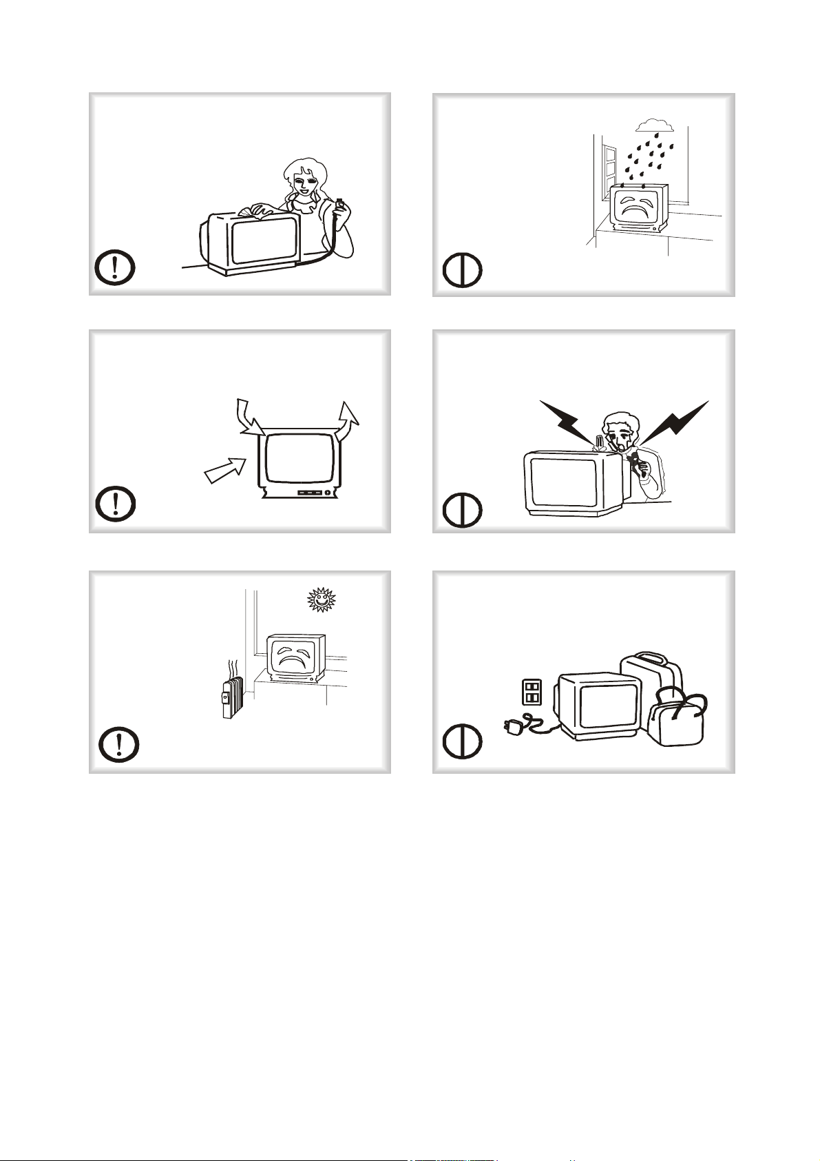
Warning and Cautions
1. When you clean the TV set, please pull
out the power plug from AC outlet. Don't
clean the cabinet and the screen with
benzen e, petrol a nd other chemical s.
2.
In order to prolong the using life of the
TV set, please place it on a ventilated
place.
4. To prevent the TV set from firing and
electric sh ock, don't
make the TV set rain
or moistu re.
5. Don't ope n the back cover , otherwise it is
possib le to dama ge the c ompon ents in the
TV set and ha rm you.
3.
Don' t place the
TV set in the
sunshine or near
heat source .
6. When the TV set i s n't going t o be used
for long time or it is in thunder and
lightening, please pull out the plug from AC
outlet a nd the ante nna plug from th e cover
of the TV set.
Explanation on the display tube
Generally, it is not needed to clean the tube surface. However, if necessary,its surface can be
cleane d w it h a dry cotton cloth after cutting off the power.D on't use any cleanser. If using ha r d
clot h, the tube surf ace will be dam a ged.
CAUTION: Before servicing receivers covered by this service manual and its supplements
and addenda, read and follow the SAFETY PRECAUTIONS.
NOTE: If unforeseen circumstances create conflict between the following servicing
precautions and any of the safety precautions, always follow the safety precautions.
Remember: Safety First.
5
Page 6

General Servicing Precautions
1. Always unplug the receiver AC power cord from the AC power source before:
a. Removing or reinstalling any component, circuit board module or any other
assembly of the receiver.
b. Disconnecting or reconnecting any receiver electrical plug or other electrical
connection.
c. Connecting a test substitute in parallel with an electrolytic capacitor in the receiver.
CAUTION: A wrong substitution part or incorrect installation polarity of electrolytic
capacitors may result in an explosion hazard.
d. Discharging the picture tube anode.
2. Test high voltage only by measuring it with an appropriate high voltage meter or other
voltage-measuring device (DVM, FETVOM, etc.) equipped with a suitable high voltage
probe. Do not test high voltage by “drawing an arc”.
3. Discharge the picture tube anode only by (a) first connecting one end of an insulated
clip lead to the degaussing or kine aquadag grounding system shield at the point where
the picture tube socket ground lead is connected, and then (b) touch the other end of
the insulated clip lead to the picture tube anode button, using an insulating handle to
avoid personal contact with high voltage.
4. Do not spray chemicals on or near this receiver or any of its assemblies.
5. Unless specified otherwise in this service manual, clean electrical contacts only by
applying the following mixture to the contacts with a pipe cleaner, cotton-tipped stick or
comparable nonabrasive applicator; 10% (by volume) Acetone and 90% (by volume)
isopropyl alcohol (90%-99% strength)
CAUTION: This is a flammable mixture.
Unless specified otherwise in this service manual, lubrication of contacts is not
required.
6. Do not defeat any plug / socket B+ voltage interlocks with which receivers covered by
this service manual might be equipped.
7. Do not apply AC power to this instrument and/or any of its electrical assemblies unless
all solid-state device heat sinks are correctly installed.
8. Always connect the test receiver ground lead to the receiver chassis ground before
connecting the test receiver positive lead.
Always remove the test receiver ground lead last.
9. Use with this receiver only the test fixtures specified in this service manual.
CAUTION: Do not connect the test fixture ground strap to any heat sink in this receiver.
Electrostatic ally Sensitive (ES) Devices
Some semiconductor (solid state) devices can be damaged easily by static electricity.
Such components are usually called Electrostatic ally Sensitive (ES) Devices. Examples of
6
Page 7

typical ES devices are integrated circuits and some field effect transistors and
semiconductor “chip” components. The following techniques should be used to help
reduce the incidence of component damage caused by static electricity.
1. Immediately before handling any semiconductor component or semiconductor-
equipped assembly, drain off any electrostatic charge on your body by touching a
known earth ground. Alternatively, obtain and wear a commercially available
discharging wrist strap device, which should be removed to prevent potential shock
prior to applying power to the unit under test.
2. After removing an electrical assembly equipped with ES devices, place the assembly
on a conductive surface such as aluminum foil, to prevent electrostatic charge buildup
or exposure of the assembly.
3. Use only a grounded-tip soldering iron to solder or unsolder ES devices.
4. Use only an anti-static type folder removal device. Some solder removal devices not
classified as “anti-static” can generate electrical charges sufficient to damage ES
devices.
5. Do not use freon-propelled chemicals. These can generate electrical charges
sufficient to damage ES devices.
6. Do not remove a replacement ES device from its protective package until immediately
before you are ready to install it. (Most replacement ES devices are packaged with
leads electrically shorted together by conductive foam, aluminum foil or comparable
conductive material).
7. Immediately before removing the protective material from the leads of a replacement
ES device, touch the protective material to the chassis or circuit assembly into which
the device will be installed.
CAUTION: Be sure no power is applied to the chassis or circuit, and observe all other
safety precautions.
8. Minimize bodily motions when handling unpackaged replacement ES devices.
(Otherwise even some normally harmless motions such as mutual brushing of your
clothes’ fabric or lifting of your foot from a carpeted floor might generate st atic electricity
sufficient to damage an ES device.)
General Soldering Guidelines
Use a grounded-tip, low-wattage soldering iron and appropriate tip size and shape that
will maintain tip temperature within the range of 500 oF to 600 oF.
Use an appropriate gauge of RMA resin-core solder composed of 60 parts tin/40 parts
lead.
Keep the soldering iron tip clean and well tinned.
Thoroughly clean the surfaces to be soldered. Use a mall wire bristle (0.5 inch, or 1.25cm)
brush with a metal handle. Do not use freon-propelled spay-on cleaners.
Use the following unsoldering technique
a. Allow the soldering iron tip to reach normal temperature. (500 o F to 600o F)
7
Page 8

b. Heating the component lead until the solder melts.
c. Quickly draw the melted solder with an anti-static, suction-type solder removal
device with solder braid.
CAUTION: Work quickly to avoid overheating the circuit board printed foil.
Use the following unsoldering technique
a. Allow the soldering iron tip to reach normal temperature. (500 o F to 600o F)
b. First, hold the soldering iron tip and solder the strand against the component lead
until the solder melts.
c. Quickly move the soldering iron tip to the junction of the component lead and the
printed circuit foil, and hold it there only until the solder flows onto and around both
the component lead and the foil.
CAUTION: Work quickly to avoid overheating the circuit board printed foil.
d. Closely inspect the solder area and remove any excess or splashed solder with a
small wire-bristle brush.
Remove /Replacement
Some chassis circuit boards have slotted holes (oblong) through which the IC leads are
inserted and then bent flat against the circuit foil. When holes are of slotted type, the
following technique should be used to remove and replace the IC. When working with
boards using the familiar round hole, use the standard technique as outlined.
Removal
Desolder and straighten each IC lead in one operation by gently prying up on the lead with
the soldering iron tip as the solder melts.
Draw away the melted solder with an anti-static suction-type solder removal device (or
with solder braid) before removing the IC.
Replacement
Carefully insert the replacement IC in the circuit board.
Carefully bend each IC lead against the circuit foil pad and solder it.
Clean the soldered areas with a small wire-bristle brush. (It is not necessary to reapply
acrylic coating to the areas).
“Small-Signal” Discrete Transistor
Removal/Replacement
Remove the defective transistor by clipping its leads as close as possible to the
component body.
Bend into a “U” shape the end of each of three leads remaining on the circuit board.
Bend into a “U” shape the replacement transistor leads.
Connect the replacement transistor leads to the corresponding leads extending from the
8
Page 9

circuit board and crimp the “U” with long nose pliers to insure metal to metal contact then
solder each connection.
Power Output, Transistor Device
Removal/Replacement
Heat and remove all solder from around the transistor leads.
Remove the heat sink mounting screw (if so equipped).
Carefully remove the transistor from the heat sink of the circuit board.
Insert new transistor in the circuit board.
Solder each transistor lead, and clip off excess lead.
Replace heat sink.
Diode Removal/Replacement
Remove defective diode by clipping its leads as close as possible to diode body.
Bend the two remaining leads perpendicularly to the circuit board.
Observing diode polarity, wrap each lead of the new diode round the corresponding lead
on the circuit board.
Securely crimp each connection and solder it.
Inspect (on the circuit board copper side) the solder joints of the two “original” leads. If they
are not shiny, reheat them and if necessary, apply additional solder.
Fuse and Conventional Resistor
Removal/Replacement
1. Clip each fuse or resistor lead at top of the circuit board hollow stake.
2. Securely crimp the leads of replacement component around notch at stake top.
3. Solder the connections
CAUTION: Maintain original spacing between the replaced component and adjacent
components and the circuit board to prevent excessive component temperatures.
Circuit Board Foil Repair
Excessive heat applied to the copper foil of any printed circuit board will weaken the
adhesive that bonds foil to the circuit board causing the foil to separate from or “lift-off” the
board. The following guidelines and procedures should be followed whenever this
condition is encountered.
At IC Connections
To repair a defective copper pattern at IC connections use the following procedure to
install a jumper wire on the copper pattern side of the circuit board. (Use this technique
only on IC connections).
1. Carefully remove the damaged copper pattern with a sharp knife. (Remove only as
much copper as absolutely necessary).
9
Page 10

2. Carefully scratch away the solder resist and acrylic coating (if used) from the end of
the remaining copper pattern.
3. Bend a small “U” in one end of a small gauge jumper wire and carefully crimp it around
the IC pin. Solder the IC connection.
4. Route the jumper wire along the path of the out-away copper pattern and let it overlap
the previously scraped end of the good copper pattern. Solder the overlapped area
and clip off any excess jumper wire.
At other connections
Use the following technique to repair the defective copper pattern at connections other
than IC Pins. This technique involves the installation of a jumper wire on the component
side of the circuit board.
Remove the defective copper pattern with a sharp knife.
Remove at least 1/4 inch of copper, to insure that a hazardous condition will not exist if
the jumper wire opens.
Trace along the copper pattern from both sides of the pattern break and locate the
nearest component that is directly connected to the affected copper pattern.
Connect insulated 20-gauge jumper wire from the lead of the nearest component on one
side of the pattern break to the lead of the nearest component on the other side.
Carefully crimp and solder the connections.
CAUTION: Be sure the insulated jumper wire is dressed so that it does not touch
components or sharp edges.
WARNING
RISKELECTRIC SHOCK
DONOT OPEN
WARNING:To reduce the risk of electric shick don’t remove cover or back.
No user-serviceable parts inside refer service to qualified service personnel.
Safety of operators has been taken into consideration at the design and manufacture phase, but
inappropriate operation may cause electric shock or fire. To prevent the product from being damaged,
the following rules should be observed for the installation, use and maintenance of the product. Read
the following safety instruction before starting the operation.
The User Manual uses the following symbols to ensure a safe operation and preventany damage to
operators or properties:
10
Page 11

3.FEATURES AND TECHINICAL DESCRIPTION
FUNCTIONS :
2
1.ALL-BAND CATV (470MHz) 2.I
3.Auto and manual tuning 4.Audio/video input/output interfaces
5.Multiple picture modes selection 6.Screen saver when no signal
7 PAL DK 8.218 programs Preset
9.volume setting stored 10.Program scan
11.Child LOCK 12.Slide curtain power on/off display,improve d eye
protection
C bus control
4. Adjustment
A..Factory adjustment information
Operation method: after the appliance is switched on, make the volume value to zero.
Then press “ V- ” key on the TV set and press the DISP button on remote controller at
the same time to enter the S state. Press DISP button one times and “S” will disappear,
Repeat the first step, you will enter the D mode. Now one “D” is displayed on the TV
screen.
Press PRO- and PRO+ buttons to select items for adjustment.
Press VOL- and VOL+ buttons to adjust selected items.
Press the POWER button to switch off the appliance and go back to the normal state.
B.Maintenance menu (Table 8)
Function Function bewrite
OSDH-POS OSD Hortzontal position 14
OPT function OPTION B4
RCUT R CUT OFF 22
GCUT G CUT OFF 33
BCUT B CUT OFF 2D
GDRV G DRIVE 40
BDRV B DRIVE 40
CNTX SUB CONTRAST MAX 7F
BRTC SUB BRIGHT CENTER 52
COLC SUB COLOR CENTER FOR NTSC 40
TNTC SUB TINT CENTER 40
COLP SUB COLOR CENTER FOR PAL 02
COLD DVD COLOR CENTER (DIF) 05
SCNT Y-SUB CONTRAST 0A
CNTC SUB CONTRASRT CENTER 4B
CNTN SUB CONTRASRT MINIMUM 07
CNTD DVD CONTRAST MAX 7F
referen
ce
initializati
on
11
Page 12

BRTX SUB BRIGHT MAX 20
BRTN SUB BRIGHT MINIMUM 20
COLX SUB COLOR MAX 25
COLN SUB COLOR MINIMUM 0D
TNTX SUB TINT MAX 28
TNTN SUB TINT MINIMUM 28
ST3 SUB SHARP CENTER NTSC3.58 IN TV 19
SV3 SUB SHARP CENTER NTSC3.58 IN VIDEO 1D
ST4 SUB SHARP CENTER OTHER COLOR SYSTEM IN TV 25
SV4 SUB SHARP CENTER OTHER COLOR SYSTEM IN VIDEO 1D
SVD SUB SHARP CENTER IN DVD 1B
ASSH ASYMMETRY – SHARPNESS 05
SHPX SUB SHARPNESS MAX POINTS FROM CENTER VALUE 1A
SHPN SUB SHARPNESS MIN POINTS FROM CENTER VALUE 19
TXCX RGB CONTRAST DATA AT MAX DATA OF USER CONTRAST
OSD
RGCN RGB CONTRAST DATA AT MIN DATA OF USER CONTRAST
OSD
ABCL ABCL, 17
DCBS DCBS, 95
CLTB The data when TV mode & SOUND SYS = M 89
CLTD The data when TV mode & SOUND SYS = M 89
CLTM The data when TV mode & SOUND SYS = M AC
CLVO The data when YVU mode & SOUND SYS != M AD
CLVD The data when YVU mode & SOUND SYS = M 88
OSDA excursus 01
HPOS 50HZ HORIZONTAL PHASE 50HZ *
VP50 50 HZ VERTICAL PHASE 50HZ *
HIT 50HZ VERTICAL AMPLITUDE *
HPS SHIFT DAT OF 50/60HZ HORIZONTAL PHASE *
VP60 60HZ VERTICAL PHASE *
HITS SHIFT DATA OF 50/60 HZ HORIZONTAL PHASE *
VLIN V-LINEARITY *
VSC V-S CORRECTION *
VLIS V-LINEARITY *
VSS V-S CORRECTION *
UVBLACK
HBOW
high 4 digit is ublack low 4 digit is &vblack
VCD_1BH high 3 digit and VCD_24H
88
88
HPARA
BRTS SUB BRIGHT 00
RAGC RF AGC ADJUSTMENT 20
HAFC 1/2 AFC DATA ADJUSTMENT 86
NOIS Signal strength setting 0F
NDTC NOISE DET count (Weak -> Normal) 1F
VL1 VOLUME OUTPUT DATA AT 25% 09
VL25 VOLUME OUTPUT DATA AT 50% 3D
12
Page 13

VL50 VOLUME 100 57
VLX ??? 7F
MUTT Y-MUTE FOR SOFT START 00
STAT CONTRAST UP FOR SOFT START 00
FLG0 Flag0 44
FLG1 Flag1 70
SVM PIC1 SVM 50
VBLK V BLANKING START AND STOP POINT 00
VCEN V CENTERING 2E
UCOM 00:GND;01:R OUTPUT;10:B OUTPUT;11:MONITOR RF AGC
00
VIA ADC
PYNX Normal H.SYNC max 33
PYNN Normal H.SYNC min 11
PYXS Search H.SYNC max 22
PYNS Search H.SYNC min 1E
RCUTS RCUTS 00
GCUTS GCUTS 00
BCUTS GDRVS 00
GDRVS GDRVS 00
BDRVS BDRVS 00
AV_OPT Av option 04
OPT2 Option 2 1C
WAIT TIME Timing between power on and picture appearing 2F
CUR_CEN Curtain beginning position BB
CUR_STEP Curtain moving speed 02
AUSTP 04
MODE0 Multiple setting A9
MODE1 Multiple setting 0F
OSDF OSD frequency 68
STBG S TRAP f0 for BG 06
STI S TRAP f0 for I 08
STDK S TRAP f0 for DK 08
STM S TRAP f0 for M 08
08
SSBG 08
SSI 08
SSDK 08
SSM
SYNC 04
S TRAP HP/LP for BG S TRAP Q for BG S TRAP GD for BG
S TRAP HP/LP for I S TRAP Q for I S TRAP GD for I
S TRAP HP/LP for DK S TRAP Q for DK S TRAP GD for DK
S TRAP HP/LP for M S TRAP Q for M S TRAP GD for M
D5 D4 D3 D2 D1 D0
option
09
SYBBN 00
SYBBF 00
SYSR
02
BBCT Blue back hysteresis counter (BUS H sync detection 04
13
Page 14

VCD0 ???? 08
VCD1 D1D0:00 38M;01:38.9M?????? 01
BL25 % of ATT for Balance 25 1E
BL49 % of ATT for Balance 49 50
OV50 OSD vertical position for 50Hz 0C
OV60 OSD vertical position for 60Hz 02
HIT1 16.:9 adjust 11
HIT2 Zoom adjust 06
COLX2 3A optiomize adjust 05
PCON Run press key 0 image resume contrast 32
PBRI Run press key 0 image resume bright 32
PCOL Run press key 0 image resume color 32
PTIN Run press key 0 image resume tint 32
PSHA Run press key 0 image resume definition 32
PVOL 32
BR_BRI bright numerical value adjust 50
CO_BRI bright numerical value adjust 32
DK_BRI bright numerical value adjust 32
BK_BRI bright numerical value adjust 1E
BR_CONT Contrast numerical value adjust 64
CO_CON Contrast numerical value adjust 64
DK_CONT Contrast numerical value adjust 32
BK_CON Contrast numerical value adjust 32
V_NOISE Sound quarrel ‘snumerical value 28
V_MID 1E
V_QUIET 0F
PWR
BUS
MEM
Q501
QT01
OPT:
BIT FUNCTION
0 Hotel mode 1:welcome logo 0:haier logo
1 No use
2 V_Mute ON/OFF when CH changes(=1:ON)
3 AUDIO GAIN SW of tb1240
4 Not VT Down of AFT when No Signal(=1)
5 TINT 0:use 1:unused
6 Select TV sync(0) or MONITOR sync(1)
7 Mute of av switch key 1.use 0.no use
ABL:
BIT FUNCTION
0
ABL-Gain 00:-0.2;01:-0.4;10:-0.6;11:-0.8v
1
2 ABL Start Point 00:-0.0;01:-0.15;10:-0.3;11:-0.45v
14
Page 15

3
4
ACL ST ????????
5
6 WPS 0:Y peak limiter off 1:Y peak limiter on,105IRE
7 No use
DCBS
BIT FUNCTION
0
1
2
3
BLACK STRETCH black strecth
00:Off;01:Black stretch point,26IRE; 10 : 33 IRE; 11 : 43 IRE ???
Y GAMMA
00:Off;01:Y γ point 90 IRE,Gain –3dB; 10 : 82 IRE ; 11 : 75 IRE
4 VCD BS SW
5 VCD CORING
6 VCD BLACK
7 C TRAP Q
CLTO\CLTM\CLVO\CLVD
BIT FUNCTION
0
1
2
3
4
Y Delay Time
000:-40 nsec;001:0;010:40 nsec;011:80 nsec;100:120 nsec;101:160 nsec;110:200 nsec;
111:240 nsec
N Phase
00:USA(105 degree);01:Japan(93 degree);10:11:DVD
5 Color Y 0:Color gamma off ;1:On;
6 PN-ID Sens 0:PAL/NTSC killer sensitivity,1mVpp; 1:10mVpp
7 FID 0:Normal;1:Alwas killer off,i.e. always color on..
SYNC:
BIT FUNCTION
0 Select sync slice level for weak signal
1 Select sync separation level
2 Select H sync judgement : 0:BUS, 1:TC3
3 UNUSE
4 UNUSE
5 UNUSE
6 UNUSE
7 UNUSE
SYBBN:
BIT FUNCTION
0 UNUSE
1 UNUSE
2 Select window pulse for H lock detection
3 Select H lock detection mode
4 Select SY-DET-1 for sync dtection
5 Select SY-DET-2 for sync dtection
6 Select LPF mode for sync dtection
7 UNUSE
SYBBF
15
Page 16

BIT FUNCTION
0 UNUSE
1 UNUSE
2 Select window pulse for H lock detection
3 Select H lock detection mode
4 Select SY-DET-1 for sync dtection
5 Select SY-DET-2 for sync dtection
6 Select LPF mode for sync dtection
7 UNUSE
SYSR:
BIT FUNCTION
0 UNUSE
1 UNUSE
2 Select window pulse for H lock detection
3 Select H lock detection mode
4 Select SY-DET-1 for sync dtection
5 Select SY-DET-2 for sync dtection
6 Select LPF mode for sync dtection
7 UNUSE
FLG0:
BIT FUNCTION
0 0:NORMAL;1:PIF over modulation switch on
1 0:BPF;1:TOF
2 0:Nyquist Buzz cancel,on;2:off
3 0:Off, 1:If BB=1, RGB out is 110 IRE
4 TB1254N band pass filter switch
5 SIF FIX Select 0:fix to normal, 1:control with sound system
6 SIF 5.74 Select In D mode, aplly this bit to SIF 574
7 vco readjust when position select 0:disable;1:enable;
FLG1:
BIT FUNCTION
0 CW SW
1 V ramp bias
2 Sync. Sepa. level
3 Horizontal side blanking
4 UNSED
5 UNSED
6 1:count time clear to 20H;0:count time clear to 0H
7 1:user press key SLEEP clear time;0:no
SVM:
BIT FUNCTION
0
1
2
3
SVM gain
00:-6dB;01:0dB;10:+6dB;11:+12dB
SVM DL(svm delay)
00:off;01:-100ns;10:-60ns;11:-40ns
4 Mon、svm ??????
16
Page 17

5
6 1: SOFT CHANGE CHANNEL 0:no
7 UNUSE
VBLK
BIT FUNCTION
0
1
2
3
00:23H;01:33H;10:37H;11:41H (50Hz)
00:22H;01:30H;10:34H;11:38H (60Hz)
00:310H;01:299H;10:295H;11:291H (50Hz)
00:263H;01:254H;10:250H;11:246H (60Hz)
4
5
MODE0:
BIT FUNCTION
0 1:218 channels;0:100 channels
1 1:5060 (M system);0:tow way AV
2 0: SECAM;1:no
3 1:RGB Out-Cut Off DC;0:Y- MU T E
4 1:ALWAYS DISPLAY SOME MENU;0:SOMETIMES DISPLAY SOME MENU
5 0:ALPS 1:panasionc
6
7
SHOP OUT
00:DK;01:I;10:BG
MODE1:
BIT FUNCTION
0 0:no BG;1:yes
1 0:noI;1:yes
2 0:noDK;1:yes
3 0:no M;1:yes
4 0:when asm & search,set up VCO adjust req. ,1:only power on
0:PIF VCO adjust trigger 1: normal (12 :bit 7)
5 The algorithm of ASM. 0:ASM doesn't judge IFLOCK with case 4. 1:ASM judge IF
LOCK with case 4
6 The algorithm of ASM. 0:ASM doesn't judge Fhsync with case 4. 1:ASM judge Fhsync
with case 4
7 TINT polarity ,input to V/C/D. 0:normal 1:invert
AV _ O P T :
Byte FUNCTION
Video1 Video2 Video3
0 VIDEO DVD
1 VIDEO S-VIDEO DVD
2 VIDEO DVD VIDEO
3 VIDEO S-VIDEO DVD
4 VIDEO/S-VIDEO DVD
5 VIDEO/S-VIDEO VIDEO DVD
6 VIDEO DVD VIDEO
7 VIDEO VIDEO DVD
OPT2:
17
Page 18

BIT FUNCTION
0 lunar calendar 1:have lunar calendar ; 0:no lunar calendar
1 No use
2 1:english 0:chinese
3 AV WITH MUTE;1:yes;0:no
4 No use
5 1:super incept 0:no
6 No use
7 0:boot-strap welcome 1:no
MOD:
BIT FUNCTION
0
1
2
3 MOD.3:0 CUTOFF range:-0.65~+0.65;1:-0.65~+0.85
4
5
6
7
OSDA
BIT FUNCTION
0
1
2
3 OSD ABL: RGB ABCL 0:ABCL active for OSD 0:inactive
4
5
6
7
akb
CUTOFF
SENSITI
VITY
000:NO;001:45.75;011:38.9;100:38.0
OSD CONTRAST
00:80 IRE 01:70;02:60;03:50;
00:*9.75;01:*10.00;10:*10.25;11:*10.50
You can change the DATA with “*” mark when necessary.
5. CIRCUIT DIAGRAM
6. WIRING CONNECTION DIAGRAM
18
Page 19

21"-TSB-2IN1 Ref. Chassis(CQ0765)
XP201
1234567
SPOT
B
G
R
+9V
N301 AN7522N
12
BL301
R-10W8
XS301
2
1
BL302
R-10W8
XS302
2
1
N206
HS0038A2
VD207
S701
CH +
S702
CH S703
VOL +
S704
VOL S705
TV/VIDEO
S706
MENU
L909
!
QHXC-54F(AL)
XS601
!
C305
C306
4.7u
4.7u
C314
2.2U
V303
2SC2878A
22K
R309
2SC2878A
V301
VD301
A1015Y
1SS133
C313
47u
4.7K
R313
B6
+9V
GND
1
5V
2
IR
3
R239
270
R761
5.6K
R762
11K
R763
15K
R764
30K
R765
110K
+13V
RT601
!
XS602
PDC7RQPP6B744
1
1
(EMC)C602
!
0.1u/250V
(EMC)L602
LCL -04
!
(EMC)C601
0.22u/250VAC
!
SW601
B5
+5V CPU
R200
0
C200
47u
R235
1K
C201
0.01u
R581
10K
V555
R557
D400
0.5W12
R559
1.8K
R558
470
VD570
MTZ10A
B4
(EMC)VD603~VD606
RM11C
C606
C605
1KV 1000p
1KV 1000p
23
(EMC)L603
C603
1
LCL -04
1KV 1000p
C604
R698
1KV 1000p
7
0.5W220K
R602
7W 1R8
(EMC)N601
DRAIN1GND2VCC3FB/OCP4SYNC
RZ601
R601
0.5W220K
!
C696
F601
10u/50V
2.5A/250V
GND
VCC1OUT12GND3OUT14STANDBY5IN16GND7IN28VOL9OUT210GND11OUT2
B3
+12V
C309
R320
C310
1/2W-4.7K
0.01u
470u/25V
+5V-2
R305
C307
R308
68K
47u
270K
2.2u
C301
R301 5.6K
R303
C304
0.01
2.2K
V302
64
63
POWER
RMT-IN
U/V1L/H2KEY3GND4RESET5X-TAL6X-TAL7TEST8+5V9GND10GND11SCP-OUT12H-OUT13H.AFC14V-SAW15V-OUT16H-VCC17GND18Cb19Y-IN20Cr21EXT-AUDIO122C-IN23EXT-IN24ALC FILTER25TV-IN(1Vp-p)26ABCL-IN27AUDIO-OUT128AUDIO-OUT229TV-OUT(2Vp-p)30SIF-OUT31EXT-AUDIO2
R582
10K
ON
OFF
C1815Y
B6
+9V
VD571
1SS133
C570
4.7u
N602A
TLP421
C607
150u/450V
VD608
EU2A
L605TEM2011
CQ0765RT
C697
1000p/1KV
R681
2W-1K
10u/50V
5
R695
0.25W470
VD682
MTZ18C
L
C3022.2u
R302 5.6K
R
C303
R304
2.2K
R314
0.01
C312
R312
47K
0.1UF
22K
C311
VD306
2.2U
1SS133
N202
3
2
1
R207
V556
!
2
3
C681
VD302
VD305
1SS133
1SS133
NM24C08EN
R228 10K
5
VSS4SDA
6
A2
SCL
R22910K
7
C250
R230
A1
TEST
47
10u
8
A0
VCC
C249
0.01u
R234
22K
R233
22K
C247
100P
60
59
61
62
VT
AV SW
SYSTEM
TV SYNC
C202
0.01u
1K
C203
CH20p
R205
R209
33K
1K
V203
A1015Y
R210
4.7K
R570 1W 27
N205
1
3
7808
C520
C521
0.01u
2
470u/16V
1
R697
4
3W 56K
22n/630V
47n
C694
VD699
TRG1C
VD696
OPEN
C698
220p/1KV
C695
OPEN
R693
1W 5.1R
VD698
EU2A
VD697
EU2A
R694
1W 1.5K
VD695
C693
1SS133
3900P
57
58
SCL1
SDA1
(EMC)
C205
G201
10u
8M
C204
CH20p
R237
1.5K
R236
8.2K
VD201
HZ3.6V
H.VCC
+8V
C522
0.01u
R645
0.25W 1K
T601
BCK-05I-5
!
1 14
C699
3
5
7
!
R531
12M
!
C615 AC400V2200p
VD251
HZ10
L207
PL-10uH
C245
C244
10u
0.01u
55
54
52
53
56
5V
GND
MUTE
D GND
R446
C207
C206
10K
8200P
0.01u
L201
10u
VD420
RD9.1CB
R699
0.25W 1K
C622
VD621
!
RU4YX
2200u/25V
R6212W 1
C621
470p/2KV
9
W608
VD625
EU2A
0.5W10
11
470p/1KV
C629
VD622
!
R631
RU4YX
0.5W 0.22
13
C624
2200u/25V
C623
470p/1KV
C627
470p/2KV
10
12
VD624S2L60U
C600
100P
C625
8
VD623
RU4YX
!
!
2200u/35V
N204
7805
H.VCC
1
3
+8V
VD253
VD252
HZ10
HZ10
R226
R225
270
270
R211
8.2K
C208
0.47U
B3
+12V
0.47u(M)
C610
B7
+180V
C630
22u/250V
V5992SB892
R598
10K
1KV 470p
R628
0.5W 2.2
C626
+5V-2
2
L209
Sin1SW2G3SO4SO
PL-12uH
VD261
MTZ5.6C
C252
R217
0.5W 270
C239
C240
10u
0.01u
R227
270
49
R-OUT50G-OUT51B-OUT
D Vcc3.3V
N201
TMPA8873
C209
470u
0.22u(M)
C210
VD681
MTZ5.1B
1
B4
+13V
C640
R462
220u/160V
18K
R599
1K
R596
10K
R5973K9
C251
0.01u
100u
C235
C234
100u
0.01u
C237
0.22u
C236
2200P
1u
L205
220K
C238
R223
R224 30K
42
43
46
47
48
44
45
YC 5V
RF AGC
APC FIL
SYNC-OUT
BLACK DET
MONITOR-OUT
C212
C214
R213
C211
0.01u
L212
47u
R595
0.25W-1K
N705
TA7805
2
C568
470u/16V
R639
0.5W 150k
RP601
20K
C643
R640
3.6K
V598
2SB892
R215
0.1u(M)
100
100
0.1u(M)
VD204
R212
OPEN
100
C213
R214
1u
100
R813
1K
VD264
H.VCC
MTZ5.6C
+8V
C223
2.2u 50V
VD614
1N4148
VD641
1N4148
3
B5
+5V CPU
C569
0.01u
B1
+115V
R643
39K
K
0.15u
R
A
N604
KA431LZ
VD599
1N4148
R115
15k
DK/I/BG
Z101
N6283
5
L204 PL-12uH
R222
40
IF IN41IF IN
IF GND
R216
100
C216
0.47u
C215
10u
R201
1M
Input1Vcc2Pump Up3GND4Output5Out Vcc6Reference
R401
16K
C401
2700p
C409
220u/35V
B2
+27V
+115V
R110
10K
VD101
1SS133
V102
C1815Y
M
C229
C230
470u
0.01u
C231
C233
C232
4.7u
2.2u
OPEN
39
37
38
S-REG
IF AGC
AUDIO MON
VD202
C219
1SS133
0.1u(M)
10u
C220
C248
R218
0.47u
100K
C221
0.1u(M)
L
N401
C402
NC
C403
0.22u
R402
0.5W 1
C407
VD401
R405
62K
R407
10k
W401
OPEN
B6
R1282W12K
+33V
N121
C126
C125
uPC574J
AGC 1VT 2SCL 4SDA 5MB 6IF
1000P
10u 50V
R100
220
R111
6.8K
R107
L103
OPEN
C104
1uH
0.01u
R112
R106
2.2K
R109
390
0
C105
C103
0.01u
V101
2SC2216
C106
R108
OPEN
VD263
R231
1.5M
MTZ5.6C
R232
OPEN
R221
750
NP 10u
C227
C226
0.47u
C2281000P
35
34
36
SIF-IN33DC NF
PIF PLL
IF-VCC(5V)
C255
47u
32
VD205
R250
OPEN
100
R811
1K
R241
A1015Y
C224
3.3K
2.2u 50V
R
B6
+9V
STV9302A
R404
12K
7
R403
C404
5.6K
10u/16V
VD402
1N4761A
L401
TEM2011
100u/35V
EU2A
R406 47K
C405
25V/0.47u
C406
1000u/25V
R409
1.2k
R412
0.68
W402
OPEN
ADS3+33V
W109
SHORT
R103
OPEN
R130
1K
C102
0.01u
R105
0
R102
R113
1.5K
3.9K
15K
C130
R114
C109
MTZ5.1B
100k
4.7u
C108
C107
220u
0.01u
33
C225
0.01u
R220
4.7K
C257
R242
330
V204
0.01u
R246
150
R247
150
X203
A1015Y
L10.7M
R219
100
R263
3.3K
V214
R408
150
C408
100V 0.047u
V431
2SC2383
R434
R432
1K
330
R433
330
C431
500V3900p
+9V
C-IN
C
U101
9
11
L104
68uH
R245
1K
V205
C1815Y
R244
330
R243
2.2K
C412
0.39u630V
V432
!
2SD2499
C416
C415
2KV 680p
2KV 6800p
T402
BCT-02
C432
1000p
C433
L405
47u/35V
ZZ0008
R435
2W 270
R439
0.5W 20K
R810
R800
560
0.5W 100
C807
V805
22u 16V
C800
2SC1815Y
100u 16V
R801
100
R803
R804
100
R802
220
75
C802
R806
10u
1K
V802
R805
2SC1815Y
2.2K
C440
100V4700p
R436
B1
+115V
0
R808
100K
C803
0.01u
LX37
L407
RU2A
VD413
R451
1W4.7K
+200V
6
5
3
4
1
2
10
(EMC)T401
!
JF0501-19910
C400
10u 160V
XS801
Y
C801
470u 10V
VD266
MTZJ3.6A
R817
75
HV
KFC
KSC
7
XS802
V-OUT
L-OUT
AV-OUT
R-OUT
R807
75
VIDEO1 IN
R809
75
AUDIO1 IN(L)
R814
OPEN
AUDIO1 IN(R)
R812
OPEN
Y
R818
75
Cb
R819
75
Cr
L410
LHDY
XS401
5
4
4
3
3
2
R413
1
0.5W4.7K
1
C411
1uF/160V
XP402
4
3
HEAT
2
1
R460
0.5W 220K
C423
100V 0.1u
R442
10K
R901100
560
R902
R911 100
R912
560
R921
R922
560
B
R
G
SPOT
XS901
R904
15K 2W
VD901
1N4148
V901
2SC2482
R903
C901
1K
330P
VD911
1N4148
V911
2SC2482
R913
C911
1K
330P
VD921
1N4148
100
V921
2SC2482
R923
C921
330P
1K
R931
1.2K
VD950
MTZ10A
R932
2K7
+
C931
L901
10u/16V
PL-12uH
GND
1234567
9V
GND
AV (Pin 61)
OSD Pin 61(N201)
TV
AV1
AV2
DVD
R905
0.5W1.2K
R915
R925
R914
15K 2W
VE1A CRT SOCKET
R924
15K 2W
R927
R935
10K
V933
2SC1815
C933
R936
0.01u
47K
VD931
VD932
SHORT
SHORT
R933
330
SYS(Pin 59)
SYS Pin 59(N201)
0V
M
0V
D/K
5V
I
0V
B/G
0.5W1.2K
RF10-1W-4.7
XS903
XP903
2
2
1
1
VE1 CRT
0.5W1.2K
C902
2KV 1000P
XS902
200V
4
3
HEAT
2
1
GND
R940
33
C932
47u/16V
V931
R934
A1015
1K
0V
5V
5V
5V
Page 20

Page 21

7. Circuit Explanation
1、Microprocessor and Small signal processing: super monolithic integrated circuits :
Haier8873
Haier8873CSN is super large integrated circuit decoder, containing intermediate image
amplifying, intermediate sound amplifying, horizontal and vertical scan, small signal
processing, color decoding, hi-pressure tracing and over-load protection, I2C bus control.
Information introducing functions and testing data for maintenance is listed in Table 1.
Table 1
Step Function
U/V
1
L/H
2
KEY INPUT
3
DIGITAL GND
4
CPU RESET
5
X.TAL
6
X.TAL
7
TEST
8
+5 VCC
9
GND
10
SIGNAL GND
11
HORIZONTAL SYNC SIGNAL INPUT
12
HORIZONTAL RETURN PULSE
13
SIGNAL INPUT CHARACTER
HORIZONTAL LOCATION
HORIZONT AL AFC
14
VERTICAL SIGNAL PRODUCE
15
LOCATION
VERTICAL RETURN PULSE SIGNAL
16
INPUT CHARACTER VERTICAL
LOCATION
17 HORIZONTAL VCC
18 GND
19 Cb SIGNAL INPUT
20 Y SIGNAL INPUT
21 Cr SIGNAL INPUT
22 EXT AUDIO
23 COLOR SIGNAL INPUT
24
EXTERIOR VEDIO SIGNAL INPUT2
Working
Voltage
(V)
0 600 5000
1.8 600 5000
5 600 15000
0 0 0
5 600 10000
2.3 600 1000
2.0 600 15000
0 0 0
5 400 4500
0 0 0
0 0 0
1 750 150
1.7 500 550
6.3 750 1400
4.3 750 1500
5.3 750 1300
8.7 100 100
0 700 900
2.4 750 5000
2.4 750 5000
2.4 700 4500
0 0 0
0 0 0
2.4 700 4500
Ground Resistance (R)
Positive
(Ω)
Negative
(Ω)
25
ALL FILTER 3.4 320 300
VEDIO SIGNAL INPUT
26
ABCL-IN
27
AUDIO OUTPUT 1
28
2.6 750 5000
4.5 750 5000
3.5 750 1400
19
Page 22

AUDIO OUTPUT 2
29
TV OUTPUT
30
SIF SIGNAL OUTPUT
31
EXTERIOR AUDIO 2
32
SIF SIGNAL INPUT AND LEVEL REVIS
33
DC FEEDBACK
34
PIF PLL
35
+5 IF VCC
36
S-REG
37
AUDIO MON
38
IF AGC
39
IF GND
40
IF INPUT
41
IF INPUT
42
RF AGC
43
BLACK DET
44
MONITOR OUTPUT
45
APC FIL
46
YV 5V
47
48
SYNC OUT
8.8 100 100
3.6 700 950
1.8 700 2100
4.3 750 1400
2.9 750 5000
2.2 750 1400
2.4 500 1500
5 750 1100
2.1 750 4000
4.4 700 1400
1.7 0 5000
0 650 0
0 650 4500
0 750 4500
3.5 500 1400
5 600 1100
1.9 650 2200
1.8 750 5000
5 0 5000
100 0
1.8
VCC
49
RED SIGNAL OUTPUT
50
GREEN SIGNAL OUTPUT
51
BLUE SIGNAL OUTPUT
52
TV SIMULATE GND
53
GND
54
+5V VCC
55
MUTE
56
I2C SERIAL BUS DATA LINE 0
57
I2C SERIAL BUS COLOCK LINE 0
58
SYSTEM
59
TUNE VOLTAGE
60
AV CHOICE CONTROL
61
HORIZONTAL SYNCHRONIZATION
62
SIGNAL
REMOTE CONTROL INPUT
63
POWER
64
3.3 750 100
2.9 750 1100
2.9 750 1100
3.1 0 1100
0 0 0
0 400 0
5.1 600 4500
0 600 7500
0 600 12500
0 600 12500
0.1 600 12500
4.4 600 10000
0.2 600 10000
4.5 600 12500
5 600 12500
3.6 600 8000
1.Analysis of common path circuits
High frequency television signals, received via an antenna (or transmitted through a cable
TV system) to the input terminal of the high frequency tuner A101, are processed for
tuning and high frequency amplifying and mixing, then a 38.9MHz image intermediate
frequency and 34.4MHZ and intermediate frequency signal will be released at the IF
terminal of Z101 to b of the transistor V101, where signals are amplified to compensate for
the insertion losses of the sound surface wave filter. Single or dual-ended input is used for
20
Page 23

the sound surface wave filters Z101 of this appliance according to system properties.
Intermediate frequency signals will be transmitted to (41) and (42) of N201(HAIER8873).
The mixed signals of picture video signals and secondary sound intermediate frequency
signals output from (31) of N201, After sound carrier frequency is trapped by the trap filter,
intermediate frequency signals are amplified and PLL image decoded, The AGC time
constant is dependent on C233 (2.2u) connected to (39) of N201 (HAIER8873),.
2.Analysis of sound power amplifying circuits
Sound power amplifying circuits are composed of integrated circuits AN7522N and
peripheral components. AN7522N is an integrated electrical circuit . Information
introducing functions and testing data for AN7522N maintenance is listed in Table 4. T if a
cylindrical color card is installed then a fluke III digital multimeter is used.
Grounding Resistance (R)
Positive
(Ω)
Negative (Ω)
No. Function
Working
Voltage (V)
1 VCC 12.56
2 OUT1+ 6.52
3 GND 0
4 OUT1- 6.52
5 STANDBY 3.75
6 IN1 1.43
7 GND 0
8 IN2 1.43
9 VOLUME 1.99
7 GND 0
8 IN2 1.43
9 VOLUME 1.99
3.Analysis of vertical sync and vertical scan output circuits
The field sync signals segregated from compound sync signals are used to activate the
vertical frequency segregation system which commences when a set amount of vertical
sync pulse signals are tested. Of the sync pulse frequencies obtained from segregation,
some are transmitted to the vertical tooth wave generator. The vertical frequency tooth
wave, after geometric processing, is transmitted from (16) of N204 (HAIER8873) to (5) of
vertical scan output IC N401 (STV9302A). The external resistor R443 (5.6KΩ) of N201 (16)
provides a reference current to the vertical tooth wave generator. The external capacitor
C244 (0.1uF) of pin (2) forms the vertical ramp wave. The vertical ramp wave is sending
the pin (4) of the vertical scan output integrated circuit N401 that is a complete bridge
current drive output circuit. After shaped and amplified the vertical ramp wave is output
from pin (2) of N401.
Information introducing functions and testing data for STV9302A maintenance is listed in
Table 4. if a cylindrical color card is installed then a fluke III digital multimeter is used.
Table 5
Grounding Resistance (R)
Positive
(Ω)
Negative
(Ω)
No. Function
Working
Voltage
(V)
21
Page 24

1 input 2.61 0 0
2 VCC 26.56 0.45 1.9
3 PUMP UP 2.21 0.5 ∞
4 GND 0 0.9 1.25
5 output 16.31 0.68 1.75
6 OUT VCC 26.87 0.5 2.95
7 reference 2.62 0.65 1.3
4.Analysis of horizontal sync and horizontal scan output circuits
As the horizontal oscillation circuit is installed inside N201 (HAIER8873), Some brightness
signals including compound sync signals are transmitted to the internal sync segregation
circuits, where horizontal sync and vertical sync pulses are segregated. R321 (10K), R462
(12K) 、C452 (3900pF) 、VD436 and T401 are connected to N201 (13) are phase-lock
loop filters. Horizontal pumping signals are transmitted from (13) of N201 to horizontal
promotion transistor V431 (2SC2383), and then drive the H-DRIVE transformer. After
being amplified through it switches power transistor V432 (2SC5885) to control the
horizontal scan of the electronic-beam.C412 is a horizontal S correction capacitor and
L407 is for horizontal linear inductor. T401 is a horizontal output transformer. The
horizontal return pulse output from (7) of T402 is transmitted to pin (27) of N201 who
controls ABL circuits. ABL avoid high-voltage over rated value that will cause X-ray and
affect your health.
5.Analysis of video amplifying circuits
The video amplifying circuits are comprised of V901, V911, V921 and peripheral
components. R, G and B signals output from N201 (50), (51) and (52), 3 video power
transistor are available for amplifying the input R, G, B. White balance adjustment is
completed through N202 under control of an I2C serial bus control system.
8. Maintenance Service and Trouble shooting
A. Principle integrated circuits
A1. 21 INCH color TV set composed of the following sections
(1) Small signal processing: super monolithic integrated circuits N201(Haier8873).
and memory N202 (AT24C08).
(2) Sound power amplifying: integrated circuits N301 ( AN7522N).
(3) Horizontal and Vertical scan output circuits: Vertical output integrated circuits
N401 (STV9302A), Horizontal output transistor V432 (2SC5885), Horizontal
flying back transformer T401 (JF0501-19910).
(4) Switch power supply: switch transformer T601 (BCK-05I-5), power IC N601
(CQ0765).
22
Page 25

A2. Main integrated circuits:
p
(1) Haier8873 Microprocessor
Picture IF/sound IF/video processing/H and V
Scan/color decoding
(2) STV9302A Vertical output integrated circuits
(3) AN7522N Sound power amplifying integrated circuits
A3. Error Detection Process
1.
Normal
Normal
The failure of horizontal
The failure ofhorizontal unit
unit orN201
orN204
Check to see
if , 8v,
5v is normal
Normal
Check VD604~VD607,
C607, N601, N604 etc.
Check to see if the
collector voltage of V598
is 27V
Check the control
voltage of V599 or
CPU
Check N202 ,ect
No light and sound
Check to see if
Fuse is normal
Normal
Abnormal
ower pin
Abnormal
Normal
Check switch
Abnormal
Check to see 110V、180V
etc. voltage is normal
Abnormal
T est to see all terminal
Resistance of load
power unit
Normal
Check the
Loader
Check to see if
rectifying tube
is normal
Abnormal
Abnormal
Change
rectifying diode
23
Page 26

2
Normal
Check the voltage
of all pins of XS903
Normal
Video amplifying
board is abnorma
Normal
Test filament voltage Test the base voltage of V431
Whether G2 voltage is normal
Abnormal
Heater Resistor
open
Abnormal
Inspect the circuit
l
from pin50 、51、
52 of N201 to
video amplifying
Normal
Check to see if +8V
voltage is normal at
PIN 17 of N201
Check G201、N201 and
peripheral circuit of N201
No raster
Check to see if be
voltage of V432 is
NO
Check the voltage
of V432 collector is
Higher
T401,VD415 or
C415,C416 are
Change wrong component
or check peripheral circuit
Normal
Abnormal
Normal Abnormal
Check the circuit
from pin13 of N201 to
existed?
YES
InspectT401、R436
normal
Lower
V432 is not well
welded or open
Abnormal
Abnormal
Check +8V power supply
V431
etc
.
24
Page 27

f
p
y
0
3
Yes
Change N201 and
repair circuit
Normal
4.
Enter D-MODE or enter
S-MODE with customer
remote controller. Make
RAGC tuned to 25 or so.
Noise on picture just
Yes
Check to see if the voltage of
pin 15 and pin16 of N201 is
normal
Not exist
Check to see if RAGC is
Yes
disappears.
Horizontal bright line
Make R328 open. Multimeter is at range RΧ1K. Red
probe connects to ground. Touch No.5 of N401 with
black probe. Bright line flashes for a moment
Check to see if voltage of pin6 at
N401 is normal
No
Inspect N201
and peripheral
components of
N2
1
at 00 mode
Z101、N20and PIF
Check to see if the deflection
yorks are connected, C433 is
peripheral component of N401
No sound and picture
Snowy noise exist
No
Inspect V101、
part
Yes
open or weldless. Inspect
and N401 itsel
Check to see if voltage
output available at tuner
Yes
Antenna
or tuner is
abnormal
No
No
Inspect +27V
ower suppl
Exist
No
Inspect the
circuit from
CPU to tuner
25
Page 28

5
6.
Picture exists but no sound
Make C305/C306 open. Multimeter is at band RΧ1K. Red
probe connect to ground. Touch No.6 OR No.8 of N301 with
No noise
Power amplifier is abnormal.
Inspect N301 and peripheral
Inspect N201 and peripheral
Change V901 or
weld V901 again
components of N301
Inspect C301、C302
Yes
component of N201
Check to see if V901 is
open or not well welded
Yes
Make C301 OR C302 collector
open. Touch No.6 OR No.8 of V301
Yes
Lack of red
Inspect R902,R903,R904
with black probe to see if noise
Check to see if voltages of XS901
No
Inspect Inspect the circuit from
are normal
Have noise
No
Check to see if
+11V exists
No
Inspect +11V
power supply
No
Yes
No.50of N201 to No.3
of XS903
26
Page 29

Troubleshooting
Before calling service personnel, please check the following chart for a
possible cause to the trouble you are experiencing.
Symptom
TV is not
turned on
Good picture ,
no sound
Poor color / tint,
good sound
Spots appear
on the screen
Lines appear
on the screen
Double images
or ghosts
Snowy picture or
black screen
Check these things
Be sure t he power cord is plugg ed in .
The MUTE f unction may be used.
Adjust the volume of the TV set.
The cont rast, color and tint m ay be incorrectly ad ju st ed.
If you change t he direction of the TV while the TV is on, the picture
may suffer from color shading. If so, turn off the TV and allow about
30 minut es to cool, t hen turn on the T V again.
The broadcast signal may be jammed by other electrical sources such
as cars, motorcycles, electric trains, high tension lines, neon signs, hair
dryers.
The broadcast signal may be jammed by other TV receivers, personal
compu ters, and T V games, as well a s interferen ce from radio stati ons.
Interference may be due to broadcast waves reflected from m ountains
or buildings.
Check if the direction of the antenna is changed.
The anten na may be disconn ected or falling out.
Check if the di rection of the antenn a is changed.
The bat t er ies in the remote control may be exha uste d.
The batteries may be improperly installed.
Check if there are obstacles between the remote control and the
remote (infrared ray) receiver.
Check if there is strong light int er f erence around the rem ot e ( in frared)
receiver.
Check if the main power is ON.
The following conditions are not troubles
Clacking noise inside
the receiver
Uneven colour in a
certain portion of the
screen
It may result fr om the e xpans ion of the shell cau sed by a tempe rature
change . This wi ll not af fect t he pictur e and so und q uality .
If the picture is too bright, this may occur according to the nature of
the pictures. Reduce the contrast, it may resume to normal.
CAUTION
In case of problems , have your T V serviced by qualified personne l. Never
attem pt to service the set yourself since opening the cabinet may expose
you to dangerous v oltage or other hazards.
27
Page 30

Sincere Forever
Haier Group
Haier Industrial Park, No. 1, Haier Road
266101,Qingdao,China
http://www.haier.com
28
 Loading...