


SUBJECT TO CHANGE WITHOUT PRIOR NOTICE © 2015 - GT-TRONICS REV 05 2016-02-02
CC264BPA-S_Bluetooth LE Module
Features
Fully compliant to Bluetooth Smart (4.2 Low Energy single mode) specifications
High efficiency on-module printed PCB RF antenna (CC264BPA-S)
Very few external BOM-count to create a fully functional application circuit
Texas Instrument CC26xx SimpleLink
TM
Wireless MCU
48MHz ARM Cortex-M3 MCU core for applications with 128K flash memory for ISP
8-KB SRAM for Cache and 20-KB Ultra-Low Leakage SRAM
Dedicated ARM Cortex-M0 core, 4KB SRAM, and ROM for RF operations
Dedicated processor and 2KB SRAM for ultra-low power sensor control
Coin batt e ry-friendly 1.8-3.8V operatio
n
Ultra Low power consumption, 6.5mA during Active-TX at 0dBM
Increased modulation index providing possible range of 100m+ in open area
Continuous Time Comparator and Ultra- Low Power An al og Comparat or
TRNG and AES-128 encrypti on for data encryption and authentication
4 General- Purpose Timer Modules (8 × 16-Bit or 4 × 32-Bit Timer, PWM Each)
Programmable UART, SPI, I2S, I2C, and GPIO interface
12-Bit ADC, 200-ksamples/s, 8-Channel Analog MUX and battery monitor
Support for 8 Capacitive Sensing Buttons
Support user-developed applications and custom profile over GATT
Integrated RF Shied can models available (CC264BPA-S / CC265BPA-S)
Bluetooth Certification BQB: Available upon request
FCC Certification: Available for CC264BPA-S
REACH / RoHS compliant
Applications
Internet of Things (IoT) Device
iBeacon
Wireless Keyboard and Mouse
GamePad and Game Controller
HID applications
Mobile phone and tablet accessory
Medical and healthcare monitor
Sports and Fitness equipment
Proximity and Lost-prevention Key Fob
Smart Wearable
RC and Interactive Toy
Home/Building Automation
Machine-to-Machine data transfer
Remote Sensor Network
Wireless Alarm and Security
Automatic Meter Reading (AMR)
Electronic Shelf Labeling
Lighting and HAVC control
Remote Control and Assisted Living
SUBJECT TO CHANGE WITHOUT PRIOR NOTICE © 2015 - GT-TRONICS REV 05 2016-02-02
General Electrical Specification
Absolute Maximum Ratings
Ratings Min. Max.
Storage Temperature
-40 ℃ +90 ℃
Supply Voltage VDD
-0.3 V 3.9 V
Recommended Operating Condition
Operating Condition Min. Max.
Operating Temperature range – (C-grade)
-20 ℃ +75 ℃
Operating Temperature range – (I-grade)
+
-40 ℃ +85 ℃
Supply Voltage VDD, VDDIO
1.8 V 3.8 V
Parameter Description Min. Typ. Max. Units
Operating Frequency
2.4GHz
Carrier frequency 2379 to 2496 MHz, 1 MHz step
40 channels
Modulation Method 1Mbps GFSK, 160/250 KHz deviation
2Mbps GFSK, 320/500 KHz deviation
Air transmission rate 2
Mbps
RF Output Power
-20
-
3.8
dBm
RX Sensitivity
@0.01% BER
-95.5 dBm
Current Consumption – TX @ +5dBm
-
9.1
- mA
Current Consumption – TX @ 0dBm
-
6.2
- mA
Current Consumption – RX Standard
-
5.9
- mA
Current Consumption – Radio Off Active
1.6
3.4
- mA
Current Consumption – Idle LPM1 Mode
-
0.5
- mA
Current Consumption – Standby LPM3 Mode, SRAM/CPU
retention and RTC running
-
1 - uA
Current Consumption – Deep Sleep LPM4/5 Mode 0.5 0.1
- uA
Current Consumption – Connected 1 sec Connection Interval,
0dBm
9.8 uA
* Measurements are for CC264BPA
+
Contact your GT-tronics sales representative for availability
Standard Firmwares Available
Heart Rate Monitor (HRP)
Blood Glucose Monitor
Health Thermometer (HLP)
Blood Pressure Monitor (BLP)
DataExchanger (serial data transfer via GATT)
Smart Lighting Control (GATT)
SUBJECT TO CHANGE WITHOUT PRIOR NOTICE © 2015 - GT-TRONICS REV 05 2016-02-02
Pins Configurations3
PIN
NAME TYPE FUNCTION
TYPICAL USAGE1
1 GND Power Ground
2 DIO_0 Digital I/O GPIO with 4mA drive capability GPIO, Sensor control
3 DIO_1 Digital I/O GPIO with 4mA drive capability GPIO, Sensor control
4 DIO_2 Digital I/O GPIO with 8mA drive capability GPIO, Sensor control
5 DIO_3 Digital I/O GPIO with 8mA drive capability GPIO, Sensor control
6 DIO_4 Digital I/O GPIO with 8mA drive capability GPIO, Sensor control
7 GND Power Ground
8 VDD_IO Power 1.8v to 3.8v GPIO Supply Connect to VDD
9 JTAG_TMSC Digital I/O JTAG TMSC Debug port data
10 GND Power Ground
11 JTAG_TCKC Digital I/O JTAG TCKC Debut port clock
12 DIO_5 Digital I/O GPIO with 8mA drive capability GPIO, JTAG_TDO
13 DIO_6 Digital I/O GPIO with 8mA drive capability GPIO, JTAG_TDI
14 VDD Power 1.8v to 3.8v main power supply 3.3v power input
15 RESET_N Digital Input Reset, active-low, no internal pullup Resistor pull up to VDD
16 DIO_7 Digital/Analog I/O GPIO with 4mA drive capability, analog Sensor control, analog
17 GND Power Ground
18 DIO_8 Digital/Analog I/O GPIO with 4mA drive capability, analog GPIO, Sensor control, analog
19 DIO_9 Digital/Analog I/O GPIO with 4mA drive capability, analog GPIO, Sensor control, analog
20 DIO_10 Digital/Analog I/O GPIO with 4mA drive capability, analog GPIO, Sensor control, analog
21 DIO_11 Digital/Analog I/O GPIO with 4mA drive capability, analog GPIO, Sensor control, analog
22 GND Power Ground
23 DIO_12 Digital/Analog I/O GPIO with 4mA drive capability, analog GPIO, Sensor control, analog
24 DIO_13 Digital/Analog I/O GPIO with 4mA drive capability, analog GPIO, Sensor control, analog
25 DIO_14 Digital/Analog I/O GPIO with 4mA drive capability, analog GPIO, Sensor control, analog
Power Ground
26 GND
Note:
1. Typical usage is firmware dependent. Please check with standard firmware application note or your firmware
designer for the actual pin definition.
2.
Pin out for CC2640 5x5 RHB IC package.
SUBJECT TO CHANGE WITHOUT PRIOR NOTICE © 2015 - GT-TRONICS REV 05 2016-02-02
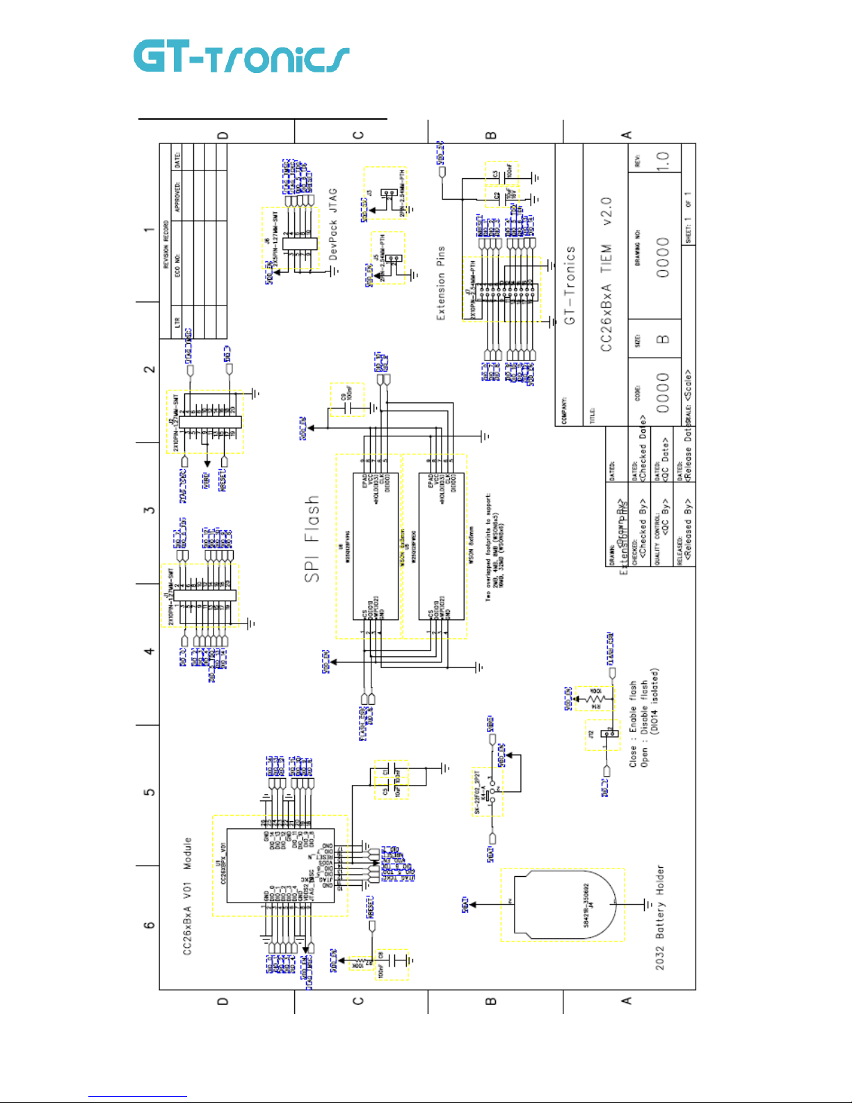
Reference Application Example

SUBJECT TO CHANGE WITHOUT PRIOR NOTICE © 2015 - GT-TRONICS REV 05 2016-02-02
CC264BPA is a high-performance and ultr
a low-power BLE 4.x data module which uses Texas Instrument’s
CC2640/CC2650 SoC as the main component. Its integrated PCB antenna further simplifies the system design to
provide users with a truly handy design block. All essential I/Os and power lines are wired out to the module pins. All I/O
functions are software configurable.
The r
eference application (TIEM) described in this section provides a typical usage example of the module. It
provides a hardware environment for CC264BPA module evaluation as well as facilitates the development of
firmware on the module. It is also compatible to TI’s SmartRF06 development board, CC2650DK Development Kit,
SensorTag Debugger DevPack, and is a near-drop-in replacement to CC2650EMK-5XD Evaluation Module. By
plugging in a CR2032 coin cell (not provided in the package) to the TIEM evaluation module, the board can run as a
standalone wireless device, providing simple function such as iBeacon. The breakout pins on the
E-interface allows further hardware feature extension. Actuator control, temperature and motion sensing, for example. This is a
perfect fit for quick prototyping Internet of Things (IoT) hardware demo.
Board Features
Featuring TI CC26xx SimpleLink Wireless SoC
Operate on battery as standalone wireless RF device
Complete BLE and Zigbee RF s olution inc l uding built-in antenna
E-interface break out pins for hardware extension
Compatible with TI SmartRF06, CC2650DK, and SensorTag Debugger DevPack
Additional Resources
See CC26xBxA Bluetooth Smart and IoT Module DataSheet for the specifications of the RF module
on the CC26xBxA Evaluation Module.
Check out Texas Instruments’ web site (http://www.ti.com) for availability of the SmartRF06
evaluation board, and SmartRF06 Evaluation Board User's Guide from Texas Instruments for the
operation of the SmartRF06 evaluation board.
Check out Texas Instruments’ web site (http://www.ti.com) for availability of the SensorTag
Debugger DevPack, and SensorTag DevPack Getting Started from Texas Instruments for the
operation of the SmartRF06 evaluation board.
Application Notes
Using coin cell battery as power source
If the TIEM evaluation module is running on CR2032 coin cell battery (i.e.VDD=3V or less), the logic
level of all IOs on E-interface will follow this VDD, which is determined by the battery level. If there is
any external hardware connected through the E-interface to the CC2640BPA module with logic levels
different from this battery level (e.g. connecting USB-UART dongle with 3.3v logic levels), power rail
mismatch problem may arise. In this case, it is suggested to supply 3.3v external power to DC power
input connection (J3) of TIEM and remove the coin cell battery.
Caution – Coin cell battery must be removed before applying 3.3V (max. allowable level) to DC
power input (J3) of the TIEM evaluation module.
Connection to JTAG debugger
CC26xBPA SMD and TIEM evaluation module support both compact JTAG (aka cJTAG) (2 wire) and
normal JTAG (4-wire). The JTAG pins on TIEM’s J6 and CC26xBPA module are (as specified in the
module datasheet):
TIEM_Pin_2, Module_Pin_11: JTAG_TMSC (used by cJTAG and JTAG)
TIEM_Pin_4, Module_Pin_13: JTAG_TCKC (used by cJTAG and JTAG)
TIEM_Pin_6, Module_Pin_14: DIO5/JTAG_TDO (used by JTAG only)
TIEM_Pin_8, Module_Pin_15: DIO6/JTAG_TDI (used by JTAG only)
Although the JTAG core signal pins (2-wire or 4-wire) are mandatory, your JTAG emulator may
requires other supporting pins to work probably. Please refer to TI's XDS Target Connection Guide
and your XDS100v3 JTAG enumerator manufacturer for the support. TIEM evaluation module’s J6
connector is a standard 10-pin ARM cortex header.
In general, in addition to the core signal pins, the following pins may need attention.
1. nRESET (Target Reset) - connect to CC2640's Reset pin (TIEM's J6 pin 10).
2. TDIS (Target Disconnect) - connect to the ground of the target (TIEM's J6 pin 9).
3. TVRef (Target Voltage Reference) - connect to the VDD of the target (TIEM's J6 pin 1).

SUBJECT TO CHANGE WITHOUT PRIOR NOTICE © 2015 - GT-TRONICS REV 05 2016-02-02
Accessing on board SPI Fla
sh
TIEM comes with 8MByte SPI flash on board which allows user to develop application that needs
storage. SPI signals CSB, MISO, MOSI and SCK are assigned to DIO7, DIO8, DIO9 and DIO10
respectively. If storage is not needed, the jumper J12 can be removed to reclaim all 4 I/Os for other
purposes.

SUBJECT TO CHANGE WITHOUT PRIOR NOTICE © 2015 - GT-TRONICS REV 05 2016-02-02
Module Outline
CC264BPA-S Module Outline
Top View Bottom View
Symbol Dimension (mm)
B 1.50
C 2.55
E 1.27
(pitch applies to all pins)
W 14.00
H 21.50

SUBJECT TO CHANGE WITHOUT PRIOR NOTICE © 2015 - GT-TRONICS REV 05 2016-02-02
Recommended PCB Land Patterns
CC264BPA-S Recommended Land Pattern (Top View)

SUBJECT TO CHANGE WITHOUT PRIOR NOTICE © 2015 - GT-TRONICS REV 05 2016-02-02
Module Reflow Installation
For RoHS/Pb-free applications, Sn96.5/Ag3.0/Cu0.5 solder is recommended.
Profile Feature Recommended Parameters
Ramp-up rate before liquidous < 2°C / second
Preheat 150-200°C 60-90 seconds
Maximum time at liquidous 40 – 80 seconds
Maximum peak temperature 230° - 240°C (below 250°C)
Ramp-down rate < 6°C / second

SUBJECT TO CHANGE WITHOUT PRIOR NOTICE © 2015 - GT-TRONICS REV 05 2016-02-02
Host Information
This module was defined to be used for specific host only. The designated host for this module was:
Company: GT-tronics HK Ltd.
Address: B210, Tonic Industrial Center, 19 Lam Hing Street, Kowloon Bay, Hong Kong
Host Model Name: TIEM
Host brand name: N/A
FCC RF Exposure Requirement
1.
At least 5mm separation distance between the antenna and the user’s body must be maintained at all times. And must not transmit
simultaneously with any other antenna or transmitter, except in accordance with FCC multi transmitter product procedures.
2.
To comply with FCC regulations limiting both maximum RF output power and human exposure to RF radiation, the antenna
gain is -0.3dBi.
3. A user manual with the end product must clearly indicate the operating requirements and conditions that must be observed to
ensure compliance with current FCC RF exposure guidelines.
Please be noticed following information and instructions should be placed in the end-user’s
operating manual
The Module has been granted as full modular approval for mobile applications. This Module must be installed in the designated
host as specified in this manual.
1. Separate approval is
required for all other operating configurations, including portable configurations with respect to 2.1093 and
different antenna configurations.
2. The Module and its antenna must not be co-located or operating in conjunction with any other transmitter or antenna within a host
device. This equipment complies with FCC RF radiation exposure limits set forth for an uncontrolled environment.
3. A label must be affixed to the outside of the end product into which the module is incorporated, with a statement similar to the
following: contains FCC ID:B4OCC264BPA-S.
4. The module shall be in non-detachable construction protection into the finished products, so that the end-user has to destroy the
module while remove or install it.
A certified modular has the option to use a permanently affixed label, or an electronic label. For a permanently affixed label, the
module must be labeled . The OEM manual must provide clear instructions explaining to the OEM the labeling requirements,
options and OEM user manual instructions that are required.
For a host using this FCC certified modular with a standard fixed label, if (1) the module’s FCC ID is not visible when installed in
the host, or (2) if the host is marketed so that end users do not have straightforward commonly used methods for access to remove
the module so that the FCC ID of the module is visible; The host OEM user manual must also contain clear instructions on how
end users can find and/or access the module and the FCC ID.
6.
Host product is required to comply with all applicable FCC equipment authorizations regulations, requirements and equipment
functions not associated with the transmitter module portion. Compliance must be demonstrated to regulations for other transmitter
components within the host product; to requirements for unintentional radiators (Part 15B). To ensure compliance with all
non-transmitter functions the host manufacturer is responsible for ensuring compliance with the module(s) installed and fully
operational. If a host was previously authorized as an unintentional radiator under the Declaration of Conformity procedure without
a transmitter certified module and a module is added, the host manufacturer is responsible for ensuring that the after the module is
installed and operational the host continues to be compliant with the Part 15B unintentional radiator requirements. Since this may
depends on the details of how the module is integrated with the host, we suggest the host device to recertify part 15B to ensure
complete compliance with FCC requirement: Part 2 Subpart J Equipment Authorization Procedures , KDB784748 D01 v07, and
KDB 997198 about importation of radio frequency devices into the United States.
5.

SUBJECT TO CHANGE WITHOUT PRIOR NOTICE © 2015 - GT-TRONICS REV 05 2016-02-02
FCC Certification Requirement:
The end product with an embedded Module may also need to pass the FCC Part 15 unintentional emission testing requirements and
be properly authorized per FCC Part 15.
Note: If this module is intended for use in a portable device, you are responsible for separate approval to satisfy the SAR
requirements of FCC Part 2.1093.
This device complies with Part 15 of the FCC Rules.
Operation is subject to the following two conditions:
(1) this device may not cause harmful interference, and
(2) this device must accept any interference received, including interference that may cause undesired operation.
Changes or modifications made to this equipment not expressly approved by GT-tronics HK Ltd. may void the FCC authorization to
operate this equipment.
 Loading...