

BC5MMRPA Class2 Bluetooth Module
Features
• Class2 module with printed PCB antenna
• Fully Qualified Bluetooth 2.1 + EDR
• CSR BC5MM-ROM chip
• Low current consumption
• 3.3V operation
• High quality 95db SNR on DAC playback
• LED drivers and faders
• Support of noise and echo cancellation
• Configurable 5-band EQ
• 802.11 Co-existence
• A2DP, AVRCP, HSP, HFP profile support
• RoHS compliant
• Dimension: 30.0 x 12.0 x 2.6 mm
Applications
• Wireless speakers
• Stereo headset
• Hands-free car kit
• VoIP handsets
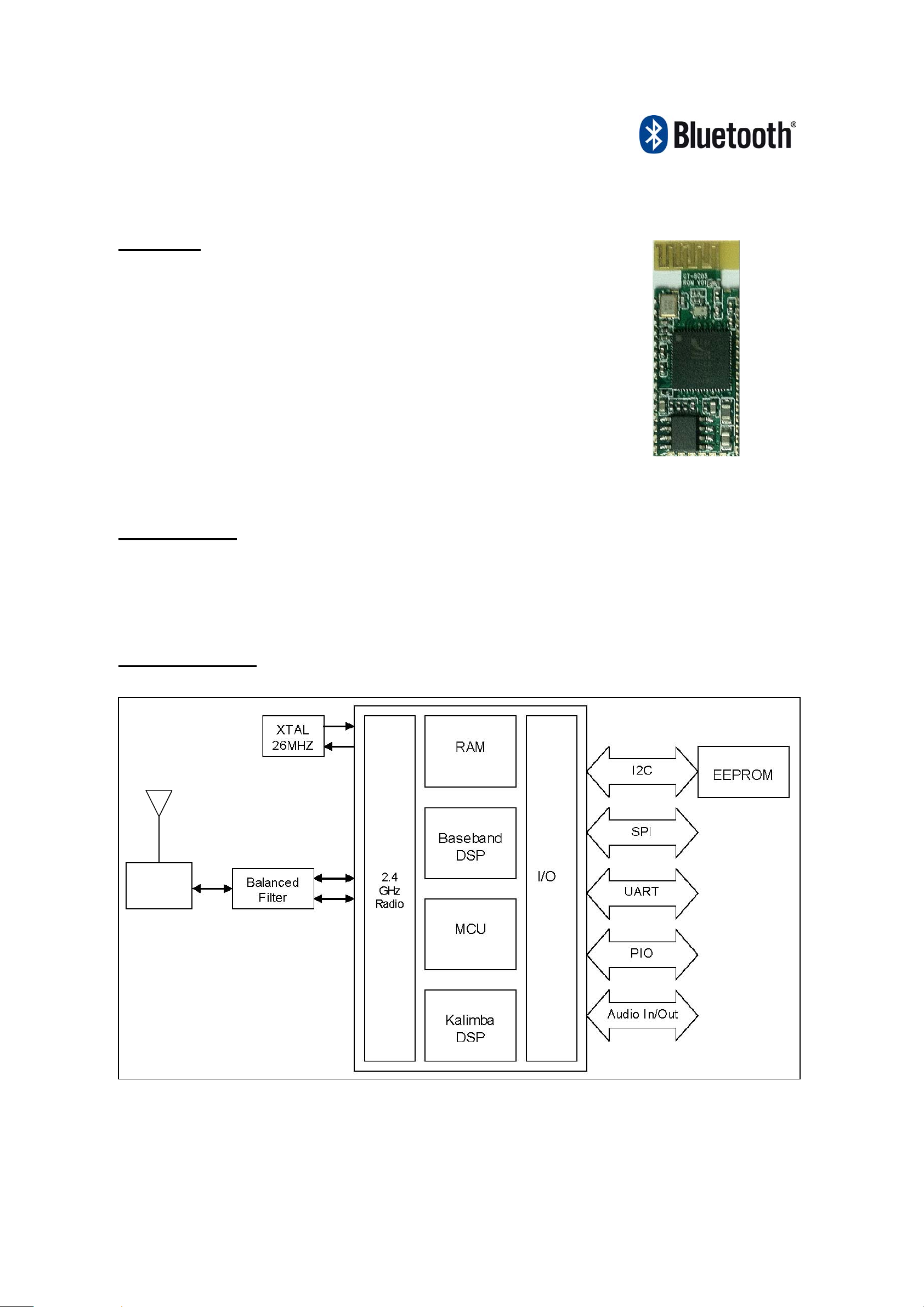
Block Diagram
PCB Antenna
2400 to 2483.5 MHz
LC Filter
BC5MMRPA is a Class 2 Bluetooth sub-system using BlueCore5 –Multimedia ROM chipset from leading Bluetooth chipset
supplier Cambrige Silicon Radio. .It interfaces to a 32-kbit EEPROM using I2C interface. The software stack running on the
BlueCore5 ROM chipset is fully compliant to Bluetooth Specification v2.1 + EDR. BC5MMRPA also has necessary balun and
bandpass filters to interface with a build-in PCB antenna, which forms a very cost effective radio subsystem.
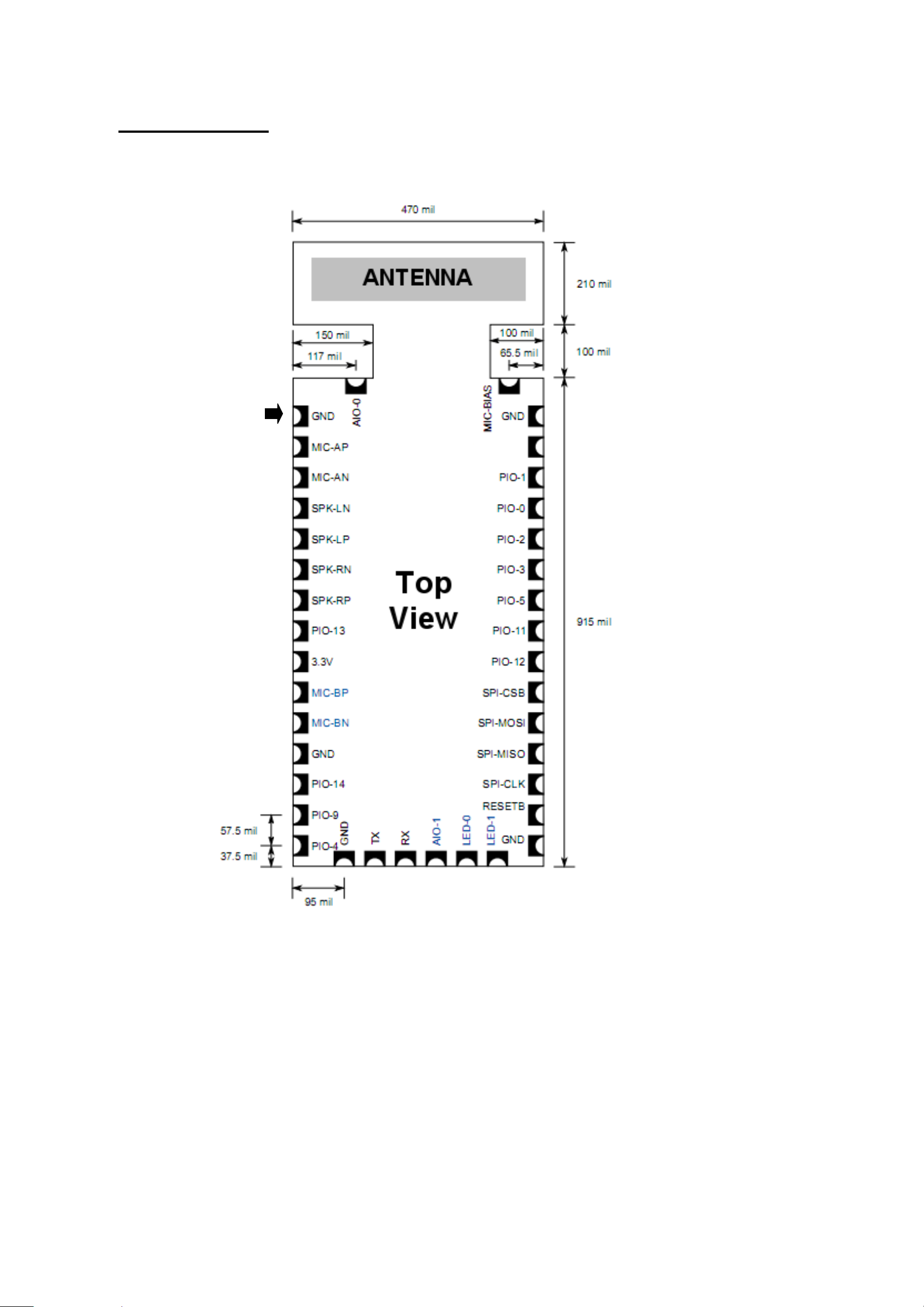
Physical Layout
Pin 1

Pins Configurations
PIN
NAME TYPE FUNCTION
1
GND GND Ground
2
MIC-AP Analogue Microphone A positive input
3
MIC-AN Analogue Microphone A negative input
4
SPK-LN Analogue Differential negative left speaker output
5
SPK-LP Analogue Differential positive left speaker output
6
SPK-RN Analogue Differential negative right speaker output
7
SPK-RP Analogue Differential positive right speaker output
8
PIO(13)
9 VDD Power
10
MIC-BP Analogue Microphone B positive input
11
MIC-BN Analogue Microphone B negative input
12 GND GND Ground
13
PIO(14)
14 PIO(9) Bi-directional Programmable Input/Output line
15 PIO(4) Bi-directional Programmable Input/Output line
16 GND GND Ground
17
UART_TX CMOS Input UART Data Output
18 UART_RX CMOS Input UART Data Input
AIO(1) Bi-directional Programmable Input/Output Line or Analogue input
19
20 LED(0) Open Drain LED driver
21
LED(1) Open Drain LED driver
22 GND GND Ground
23 RESETB CMOS input Reset if low. Input debounced so must be low for >5ms to cause a reset
24 SPI_CLK CMOS Input Serial Peripheral Interface Clock
Bi-directional Programmable Input/Output line
3.3V Power Supply Input
Bi-directional Programmable Input/Output line
25 SPI_MISO CMOS Output Serial Peripheral Interface Data Output
26 SPI_MOSI CMOS Input Serial Peripheral Interface Data Input
27 SPI_CSB CMOS Input Chip Select For Synchronous Serial Interface active low
28 PIO(12)
29 PIO(11)
PIO(5) Bi-directional Programmable Input/Output line
30
PIO(3) Bi-directional Programmable Input/Output Line
31
PIO(2) Bi-directional Programmable Input/Output line
32
33 PIO(0)
34 PIO(1)
35 NC
GND GND Ground
36
37 MIC_BIAS Analogue Microphone bias
AIO(0) Bi-directional Programmable Input/Output Line or or Analogue input
38
Bi-directional Programmable Input/Output line
Bi-directional Programmable Input/Output line
Bi-directional Programmable Input/Output line
Bi-directional Programmable Input/Output line
No connect

General Electrical Specification
Absolute Maximum Ratings
Ratings Min. Max.
Storage Temperature
Supply Voltage VDD -0.4 V 3.7 V
Recommended Operating Condition
Operating Condition Min. Max.
Operating Temperature range
Supply Voltage VDD 3.0 V 3.6 V
Parameter Description Min. Typ. Max. Units
Already Paired - TBD - mA Current Consumption - Discover
New Pairing - 5 - mA
Dist = 1m - 44 - mA Current Consumption - Playing
Dist = 10m - 50 - mA
Dist = 1m - 8 - mA Current Consumption - Pause
Dist = 10m - 8 - mA
Current Consumption - Sleep - 2 - mA
-40 ℃ +85 ℃
0 ℃ +55 ℃
Radio Characteristics
Radio Characteristics, VDD = 3.3V Temperature =+20°C
Sensitivity at 0.1% BER
Maximum received signal at 0.1%
BER
RF transmit power 1
Initial carrier frequency tolerance
Frequency
(GHz)
2.402 - -83 -82 dBm
2.441 - -83 -82 dBm
2.480 - -83 -82
2.402 - -6 0 dBm
2.441 - -6 0 dBm
2.480 - -6 0
2.402 - +2 - dBm
2.441 - +2 - dBm
2.480 - +2 -
2.402 - 12 20 kHz
Min Typ Max Bluetooth
Unit
Specification
< - 70
dBm
> - 20
dBm
-6 to +4 2
dBm
±75
2.441 - 10 20 kHz
2.480 - 9 20
20dBm bandwidth for modulated
carrier
Drift (single slot packet)
Drift (five slot packet)
Drift Rate
RF power control range 16 35 -
RF power range control resolution - 1.8 - - dB
2.402 - 879 1000 kHz
2.441 - 816 1000 kHz
2.480 - 819 1000
2.402 - 10 20 kHz
2.441 - 10 20 kHz
2.480 - 10 20
2.402 - 14 20 kHz
2.441 - 14 20 kHz
2.480 - 14 20
2.402 - 11 15 kHz/50µs
2.441 - - 15 kHz/50µs
2.480 - - 15
< 1000
<25
<40
20
kHz
kHz
kHz
kHz
kHz/50µs

△f1avg “Maximum Moudulation”
2.402 145 165 175 kHz
140<△f1avg <175
2.441 145 165 175 kHz
2.480 145 165 175
△f2maz “Minimum Modulation”
2.402 115 150 - kHz
2.441 115 150 - kHz
115
2.480 115 150 -
C/I co-channel - 10 11
Adjacent channel selectivity C/I F=F0 +1 MHz
Adjacent channel selectivity C/I F=F0 - 1MHz
Adjacent channel selectivity C/I F=F0 +2 MHz
Adjacent channel selectivity C/I F=F0 - 2MHz
Adjacent channel selectivity C/I F>=F0 +3 MHz
Adjacent channel selectivity C/I F<=F0 -5 MHz
Adjacent channel selectivity C/I F=Fimage
Adjacent channel transmit power F=F0±2MHz
Adjacent channel transmit power F=F0±3MHz
3 5
- -4 0
3 5
- -4 0
3 5
- -35 -30
3 5
- -21 -20
3 5
3 5
3 5
4 5
4 5
- -45 -
- -45 -
- -18 -9
- -35 -20
- -45 -40
<= 11
<= 0
<= 0
<= - 30
<= - 20
<= - 40
<= - 40
<= - 9
<= - 20
<= - 40
Notes:
1
2
3
4
5
PSR configuration setting maintains the transmit power to be within the Bluetooth specification v2.0 limits
Class 2 RF transmit power range, Bluetooth specification v2.0
Up to five exceptions are allowed in v2.0 of the Bluetooth specification
Up to three exceptions are allowed in v2.0 of the Bluetooth specification
Measured at F0 = 2441MHz
kHz
kHz
dB
dB
dB
dB
dB
dB
dB
dB
dBc
dBc
FCC Statement:
NOTICE:
This device complies with Part 15 of the FCC Rules. Operation is subject to the following two conditions: (1) this
device may not cause harmful interference, and (2) this device must accept any interference received, including
interference that may cause undesired operation.
Changes or modifications made to this equipment not expressly approved by GT-tronics HK Ltd may void the FCC
authorization to operate this equipment.
This equipment has been tested and found to comply with the limits for a Class B digital device, pursuant to Part 15 of
the FCC Rules. These limits are designed to provide reasonable protection against harmful interference in a residential
installation. This equipment generates, uses and can radiate radio frequency energy and, if not installed and used in
accordance with the instructions, may cause harmful interference to radio communications. However, there is no
guarantee that interference will not occur in a particular installation. If this equipment does cause harmful interference
to radio or television reception, which can be determined by turning the equipment off and on, the user is encouraged to
try to correct the interference by one or more of the following measures:
• Reorient or relocate the receiving antenna.
• Increase the separation between the equipment and receiver.
• Connect the equipment into an outlet on a circuit different from that to which the receiver is connected.
• Consult the dealer or an experienced radio/TV technician for help.
Radiofrequency radiation exposure Information:
This equipment complies with FCC radiation exposure limits set forth for an uncontrolled environment. Please see the
RF Exposure information. This transmitter must not be co-located or operating in conjunction with any other antenna or
transmitter.
This device should be installed and operated with a minimum distance of 20 cm between the antenna and all persons.
Label requirements:
Contains Transmitter Module FCC ID: B4OBC5MMRPA
 Loading...